EP1720281A1 - Verfahren zur steuerung eines steckbaren ports einer kommunikationsschmittstellenkarte und schmittstellenkarte - Google Patents
Verfahren zur steuerung eines steckbaren ports einer kommunikationsschmittstellenkarte und schmittstellenkarte Download PDFInfo
- Publication number
- EP1720281A1 EP1720281A1 EP05745099A EP05745099A EP1720281A1 EP 1720281 A1 EP1720281 A1 EP 1720281A1 EP 05745099 A EP05745099 A EP 05745099A EP 05745099 A EP05745099 A EP 05745099A EP 1720281 A1 EP1720281 A1 EP 1720281A1
- Authority
- EP
- European Patent Office
- Prior art keywords
- password
- pluggable
- interface board
- port
- pluggable port
- Prior art date
- Legal status (The legal status is an assumption and is not a legal conclusion. Google has not performed a legal analysis and makes no representation as to the accuracy of the status listed.)
- Ceased
Links
Images



Classifications
-
- G—PHYSICS
- G06—COMPUTING OR CALCULATING; COUNTING
- G06F—ELECTRIC DIGITAL DATA PROCESSING
- G06F13/00—Interconnection of, or transfer of information or other signals between, memories, input/output devices or central processing units
- G06F13/38—Information transfer, e.g. on bus
- G06F13/40—Bus structure
- G06F13/4063—Device-to-bus coupling
- G06F13/4068—Electrical coupling
- G06F13/4081—Live connection to bus, e.g. hot-plugging
-
- G—PHYSICS
- G06—COMPUTING OR CALCULATING; COUNTING
- G06F—ELECTRIC DIGITAL DATA PROCESSING
- G06F21/00—Security arrangements for protecting computers, components thereof, programs or data against unauthorised activity
- G06F21/70—Protecting specific internal or peripheral components, in which the protection of a component leads to protection of the entire computer
- G06F21/82—Protecting input, output or interconnection devices
- G06F21/85—Protecting input, output or interconnection devices interconnection devices, e.g. bus-connected or in-line devices
-
- H—ELECTRICITY
- H04—ELECTRIC COMMUNICATION TECHNIQUE
- H04L—TRANSMISSION OF DIGITAL INFORMATION, e.g. TELEGRAPHIC COMMUNICATION
- H04L9/00—Cryptographic mechanisms or cryptographic arrangements for secret or secure communications; Network security protocols
- H04L9/32—Cryptographic mechanisms or cryptographic arrangements for secret or secure communications; Network security protocols including means for verifying the identity or authority of a user of the system or for message authentication, e.g. authorization, entity authentication, data integrity or data verification, non-repudiation, key authentication or verification of credentials
- H04L9/3226—Cryptographic mechanisms or cryptographic arrangements for secret or secure communications; Network security protocols including means for verifying the identity or authority of a user of the system or for message authentication, e.g. authorization, entity authentication, data integrity or data verification, non-repudiation, key authentication or verification of credentials using a predetermined code, e.g. password, passphrase or PIN
Definitions
- the present invention relates to single boards of communication devices. More particularly, the invention relates to a method for controlling pluggable ports on an interface board of a communication device and a kind of interface board.
- a communication device is generally composed of all sorts of single boards such as system control boards, cross boards, interface boards, power supply boards, etc.
- the system control board is mainly responsible for control and management of other single boards, the system control board can be connected to a network management device and perform management functions, e.g. system configuration, via input/output devices of the network management devices, e.g. keyboards and displays.
- the cross board is connected with the system control board and the interface board, and is used for scheduling data input from the interface board, and after scheduling the data, the cross board outputs the data to the designated interface board, and the cross board is further used for executing commands of the system control board and returning relative information to the system control board.
- the interface board is connected with the system control board and the cross board, and is mainly used for inputting/outputting services, and performing a protocol processing to the services, and switching data with the cross board, executing the commands of the system control board and returning relative information to the system control board.
- the power supply board is used for supplying each single board with power. It can be seen that the capacity of the communication device is embodied through the number of the interface boards and the number of input/output interfaces on each interface board.
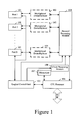
- FIG. 1 is a schematic diagram illustrating the structure of the interface board in the related art.
- the interface board includes multiple input/output ports 101, a multiplexer/demultiplexer 102, which is optional, a protocol processing module 104, a logical control module 105, a CPU processing unit 106, a memorizer 107, and a clock processing module 108.
- the interface board can communicate with the system control board or/and other single boards of the device through the bus of the CPU Processing unit 106.
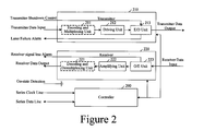
- FIG. 1 is a structural schematic diagram illustrating the internal functions of the pluggable module.
- the above-mentioned pluggable module mainly includes a controller 200, a transmitter 210 and a Receiver 220.
- the transmitter 210 consists of an encoding and multiplexing unit 211, which is optional, a driving unit 212 and an electronic/optical unit 213;
- the Receiver 220 consists of a decoding and demultiplexing unit 221, an amplifying unit 222 and an optical/electronic unit 223.
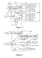
- FIG. 3 is a structural diagram illustrating a typical circuit of the pluggable port on the interface board according to the related art.
- the pluggable port mainly includes a connector 300, a power supply VCC, inductors L1 and L2, capacitors C1, C2 and C3, a multiplexer/demultiplexer 303, a logical control unit 305, a CPU 306, a protocol processor 304, and a resistors R1, R2 and R3.
- the Connector 300 is used for connecting the pluggable module and other parts of the pluggable module;
- the Power Supply VCC is used for supplying the pluggable module with power;
- the inductors L1 and L2, the capacitors C1, C2 and C3 are used for power filter;
- the multiplexer/demultiplexer 303 is used for combining multiple lines of low-rate data into one line of high-rate data and dividing one line of high-rate data into multiple lines of low-rate data in the reverse direction, herein it needs to be explained that the multiplexer/demultiplexer 303 is optional;
- the logical control unit 305 is used for detecting and controlling the logical states of the pluggable module, the multiplexer/demultiplexer 303 and the protocol processor 304;
- the CPU 306 is used for controlling the logical control unit 305 and the protocol processor 304;
- the protocol processor 304 is used for processing the input/output data;
- the Resistor R1 cooperates with Pins D and E of the
- the Pin D of the logical control unit 305 When the pluggable port of the interface board works, as shown in Figure 3, the Pin D of the logical control unit 305 outputs a high level, the Pin E of the logical control unit 305 detects the state of the input voltage level, if the high level is detected, it indicates that the pluggable module is not-in-position. After the pluggable module is plugged-in, the in-position detection line of the pluggable module will lower the voltage level, and the Pin B of the logical control unit 305 will detect the input voltage level is the low level, which indicates the pluggable module is in-position.
- each port has a set of R1, L1/L2, C1, C2 and C3. All the ports share one CPU 306, one logical control unit 305 and one or more than one protocol processor 303, and each protocol processor 303 can process one or more than one interface service. Under the circumstances of multiple ports, if one protocol processor 303 is not adequate, more than one protocol processor 303 can be adopted. Generally, the port does not need a clock processing module, so there is no clock processing module in Figure 3.
- FIG. 4 is a schematic diagram illustrating the functional structure and connective relations of the logical control unit according to the related art.
- the logical control unit 400 includes: an interface module 401, a protocol processor Control detecting module 402, a multiplexer/demultiplexer control detecting module 403, a transmitter shutdown control module 404, an alarm receiving module 405, an In-position detecting module 406 and a serial control module 407.
- the interface module 401 receives commands from the CPU 420, sends the commands to the other functional modules, and receives the information from other functional modules and returns the information to the CPU 420.
- the protocol processor control detecting module 402 performs the control and the detection to the protocol processor 410 according to the commands from the interface module 401, and returns the results of the control and the detection to the CPU 420 through the interface module 401.
- the multiplexer/demultiplexer control detecting module 403 performs the control and the detection to the multiplexer/demultiplexer according to the commands from the interface module 401, and returns the results of the control and the detection to the CPU 420 through the interface module 401.
- the transmitter shutdown control module 404 sets the transmitter shutdown control signal as valid or invalid according to a command from the interface module 401.
- one function of the CPU 420 is to send a command to the logical control unit 400 to implement the transmitting shutdown control of the transmitter of the pluggable module to according to the demand of service.
- the CPU 400 has very powerful functions, it is the control centre of the whole single board, not only controlling the logical control unit 420; other functions are not mentioned herein due to their limited relevance to the present invention.
- the alarm receiving module 405 receives the alarm information, e.g. a laser failure alarm, a receiver signal loss alarm, etc., from the pluggable module, and transmits the alarm information to the CPU 420 through the interface module 401.
- the alarm information e.g. a laser failure alarm, a receiver signal loss alarm, etc.
- the In-position detecting module 406 receives the in-position detection signals from the pluggable module, and detects whether the pluggable module is in-position, and transmits the detection results to the CPU 420 through the interface module 401.
- the serial controlling module 407 transmits serial clock signals to the pluggable module according to the commands from the interface module 401, and transmits serial data with the pluggable module.
- the logical control unit of the interface board can only perform the on-state detection to the pluggable module, and receive the alarms from the pluggable module and perform the shutdown control to the receiver of the pluggable module according to the demand of service; however, the logical control unit of the interface board can not manage the plugging-in and the replacement of the pluggable module, and it also has no efficient power control to prevent the pluggable ports of the interface board from being falsely or illegally used. So, the above-mentioned solution has the following disadvantage: when users arbitrarily add large amounts of pluggable modules, or optionally replace the pluggable modules, the device and the network are likely to be unstable.
- the present invention provides a method for controlling a pluggable port on an interface board of a communication device to avoid the pluggable port on the interface board from being falsely or illegally used.
- the present invention also provides an interface board with a pluggable port, which will not be falsely or illegally used.
- a method for controlling the pluggable port of the interface board of the communication device including the following steps:
- the process of pre-setting a password for the pluggable port of the interface board can be any one of:
- the step of storing the pre-set password includes: storing each pluggable port number and the corresponding password in the interface board;
- the verification of the password can be implemented by a CPU of the interface board.
- the step of storing the pre-set password can also be: storing each pluggable port number and the corresponding password, as well as the sequence number of the interface board corresponding to the pluggable port, into the system control board of the communication device correspondingly;
- the step of the communication device enabling or disabling the pluggable port of the interface board according to the verification result includes:
- the step of the logical control unit enabling or disabling the pluggable port according to the command from the CPU can be: the logical control unit setting a transmitter shutdown control signal as valid or invalid according to the command from the CPU.
- Switch(es) can be set on at least one of a power line, transmitter data input lines, receiver data output lines of a circuit of the pluggable port of the interface board;
- the step of verifying the received password according to the pre-stored password can be:
- the method further includes: pre-configuring a number of password input times and storing the number of the password input times together with the password;
- the method further includes: setting the state of the pluggable port of the interface board as disabled when setting password for it;
- the method further includes: storing the pre-stored password of the pluggable port and a sequence number of its interface board into a manufacture database correspondingly; and when the communication device is used, obtaining the password of the pluggable port of the interface board from the manufacture database through networks according to the sequence number of the interface board.
- the present invention provides an interface board with a pluggable port, includes at least: a CPU, a memorizer, a logical control unit, at least one kind of port line(s) connecting with a pluggable module, at least one switch, used for enabling or disabling the pluggable port wherein, the switch(es) is (are) set on at least one kind of the port line connecting with the pluggable module; the memorizer stores a pre-set password of the pluggable port; the CPU receives an external inputted password from the system control board, and verifies the received password by the pre-stored password in the memorizer, and sends a command to enable or disable the interface board to the logical control unit according to the verification result; the logical control unit enables or disables the pluggable port according to the command from the CPU.
- the port line connecting with the pluggable module can be:
- the logical control unit includes at least: an interface module and a switch control module; wherein, the interface module receives a command from the CPU and sends the command used for controlling the switch to the switch control module; the switch control module turns the switch on or off according to the received command.
- the present invention can limit the use and replacement of the pluggable port, and the pluggable port of the interface board in the present invention is allowed to be enabled only when the password is correctly inputted.
- the present invention implements the management of enabling and disabling the pluggable port by adding one or more than one switch in the pluggable port of the interface board and through the control of the logical control unit.
- the present invention can better prevent the pluggable port from being falsely or illegally used, avoid the instability and unreliability of the communication device and the communication network resulting from the false or illegal use, and guarantee the normal operation of the communication device and communication network.
- the method for controlling the pluggable port of the interface board of the communication device and the interface board is to pre-set a password for the pluggable port of the interface board to limit the use and replacement of the pluggable port.
- the pluggable port of the interface board is allowed to be enabled only when the password is correctly inputted.
- the method for controlling the pluggable port is to pre-set a password for the pluggable port of the interface board and stores the password; the process of controlling the pluggable port of the interface board includes:
- one of them does not change the hardware structure of the interface board, in which the logical control unit sets the input voltage level of the transmitter shutdown control module after the password verification is passed, to control the pluggable port.
- the other is to add switch(es) on the port line(s) connecting with the pluggable module, and to control the pluggable port through controlling the switch(es) by the logical control unit after the password verification is passed.
- the present embodiment adopts the first implementation method as mentioned above.
- the control process of the embodiment includes: a process of setting the password, a control process when detecting a pluggable module is plugged-in, and a process of configuring the pluggable port.
- the present embodiment sets one respective password for each pluggable port.
- the process of setting the passwords is implemented during manufacture; a simple method is: setting an upper limit for the number of the pluggable ports that the interface board can hold, then setting one password for each pluggable port and storing the password in the memorizer of the interface board, then setting the states of the pluggable ports to be disabled and correspondingly storing the sequence number of the interface board and the pre-set passwords into the manufacture database.
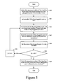
- Figure 5 is a flowchart illustrating a process of setting the passwords according to the first preferable embodiment of the present invention, including the following steps:
- the maximum number Q of password input times denotes the allowable times to input incorrect passwords, if the input times exceeds the maximum number Q of password input times, the system will not allow the user to change the state of the pluggable port any more, which will be described in detail hereinafter.
- the manufacture database is used for recording a serial of data generated during the production of devices and their single boards, e.g. device configurations, single board information, etc.
- the manufacture database is a database used for storing the data of production process of device vendors.
- sequence number is also known as a serial number, which is the only identifier of the interface board; in general, the serial number is stuck on the handle plate of the interface board in a format of bar code, and the bar code contains such information as type, production time and serial number of the interface board.
- Figure 6 is a flowchart illustrating the control when the interface board detects a pluggable module is plugged-in according to the embodiment shown in Figure 5. The process includes:
- the determination process can be: setting a state indicator in software, and determining whether the state is enabled by reading the value of the indicator.
- the determination process can also be: determining whether the input voltage level of the transmitter shutdown control module is valid, if it is valid, the state of the pluggable port X is enabled.
- the system will pop up a dialog box prompting the user to input the password, specifically: the interface board informs the system control board of the communication device when detecting that a pluggable module is plugged-in, and the system control board pops up a dialog box prompting the user to input the password through a display connecting with it.
- the system control board sends the password to the interface board after the user inputs the password.
- Step 605 the interface board determines whether the inputted password of the pluggable port X is correct according to the password of the pluggable port X stored in the memorizer of the interface board, if it is correct, go to step 606; if the password is incorrect, i.e. the password verification is not passed, go to step 607.
- the determination can be made through simply judging whether the two passwords are identical. If the inputted password is identical with the stored password, the verification is passed.
- the procedure shown in Figure 6 implements the procedure of enabling the pluggable port through inputting the correct password of the pluggable port, and meanwhile, forbidding the user who successively inputs incorrect passwords to falsely or illegally use the pluggable port of the interface board.
- the state of the pluggable port can be set to be enabled or disabled through inputting the correct password, and the false or illegal uses can be avoid.
- the present embodiment also adopts the first implementation method.
- set one share password for multiple pluggable ports i.e. each pluggable port is not uniquely corresponding to the password
- one password controls at least one pluggable port.
- the control procedure when detecting that a pluggable module is plugged-in and the setting procedure when configuring the pluggable port the control procedure of the embodiment further includes: a process of enabling the pluggable ports of the interface board and a process of modifying the number of the pluggable port that the password allows to enable.
- FIG. 8 is a flow chart illustrating a procedure of setting the password according to the second preferable embodiment of the present invention. The procedure includes the following steps:
- the procedure of setting multiple passwords for one pluggable port can be the same as the that shown in Figure 5, just more than one password set for each pluggable port; the manner only increases the data quantity to be stored without any improvement of security, so in general, the manner is not adopted.
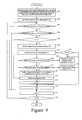
- Figure 9 is a flowchart illustrating the procedure of enabling the pluggable port of the interface board of the embodiment shown in Figure 8. The procedure includes the following steps:
- the number U of the pluggable ports permitted to be enabled denotes the total number of the pluggable ports can be enabled by all the passwords.
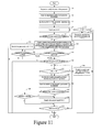
- Figure 11 is a flow chart illustrating the procedure of modifying the number of the pluggable ports that the password permits to enable as in the embodiment shown in Figure 8. The procedure includes the following steps:
- the procedure of setting the pluggable ports in the embodiment can be the same as that in the first preferable embodiment, which will not be repeated herein.
- passwords are stored in the interface board and verification is implemented by the CPU module of the interface board.
- the passwords can also be stored in the system control board of the communication device, the system control board implements the verification and sends the verification result to the CPU of the interface board, and the CPU controls the logical control unit to enable or disable the pluggable ports.
- the method will increase the load of the system control board; so generally, the passwords are stored in the interface board.
- the procedure of setting the states of the pluggable ports on the interface board to be enabled or disabled is implemented through controlling the high or low level voltage of the transmitter shutdown signal by the logical control unit of the interface board.
- the detailed control procedure is: the CPU of the interface board verifies the password, and sends the command of enabling or disabling the pluggable port to the logical control unit according to the verification result, or sends the required state for enabling or disabling the pluggable port to the logical control unit.
- the logical control unit controls the transmitter shutdown signal as valid or invalid, i.e. controls the voltage level of the signal to be high or low, according to the received command or state information.
- the system control board verifies the password, and sends the verification result to the CPU of the interface board, the CPU sends the command of enabling or disabling the pluggable port to the logical control unit according to the verification result, or sends the required state for enabling or disabling the pluggable port to the logical control unit, and the logical control unit controls the transmitter shutdown signal as valid or invalid, i.e. controls the voltage level of the signal to be high or low, according to the received command or state information.
- This embodiment adopts the second implementation method as mentioned above.
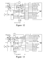
- the control procedure of the embodiment is basically the same as that of the first and the second preferable embodiments, and the difference is: in the first and second preferable embodiments, the pluggable ports are controlled through setting the input voltage level of the transmitter shutdown control by the logical control unit; while in this embodiment, the pluggable ports are controlled through controlling the switches by the logical control unit. Thereby the control procedure will not be repeated herein, and hereinafter the hardware of the present embodiment will be described in detail.
- At least one switch used for enabling or disabling the pluggable port is added to the interface board; the above-mentioned switch(es) is(are) set on at least one kind of port line connecting with the pluggable module.
- the memorizer stores the pre-set password of the pluggable port.
- the CPU receives the external inputted password from the system control board, implements password verification by the passwords stored in the memorizer, and sends the command of enabling or disabling the pluggable port of the interface board to the logical control unit according to the verification result.
- the logical control unit controls the switches to be on or off according to the command from the CPU.
- the switch(es) on the transmitter data input lines are single-line switches or is a multi-line switch, and the number of lines of the switch is the same as that of the input signals of the transmitter.
- the switch(es) on the receiver data output line are single-line switches or is a multi-line switch, and the number of lines of the switch is the same as that of the output signals of the receiver;
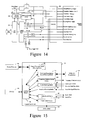
- Figure 15 is a schematic diagram illustrating the functional structure and the connective relation of the logical control unit according to the third preferable embodiment of the present invention. Comparing Figure 15 with Figure 4, it is obvious that in the embodiment, a switch control module 151 is added to the logical control unit 150, and the switch control module 151 is directly connected to the interface module 401.
- the interface module 401 determines which functional module the commands are to be sent after receiving the commands from the CPU, and transmits the command used for controlling the switches wherein to the switch control module 151.
- the switch control module 151 controls the Switch Device 152 to be on or off according to the received command.
- the method for controlling the pluggable port of the interface board of the communication device and the interface board in present invention can better prevent the pluggable port from being falsely or illegally used, thereby avoiding the instability and unreliability of the communication device and the communication network resulting from the false or illegal use, and guarantees the normal operation of the communication device and communication network.
Landscapes
- Engineering & Computer Science (AREA)
- Theoretical Computer Science (AREA)
- Computer Security & Cryptography (AREA)
- General Engineering & Computer Science (AREA)
- Computer Hardware Design (AREA)
- Physics & Mathematics (AREA)
- General Physics & Mathematics (AREA)
- Software Systems (AREA)
- Signal Processing (AREA)
- Computer Networks & Wireless Communication (AREA)
- Information Transfer Systems (AREA)
- Details Of Connecting Devices For Male And Female Coupling (AREA)
- Small-Scale Networks (AREA)
Applications Claiming Priority (2)
| Application Number | Priority Date | Filing Date | Title |
|---|---|---|---|
| CN2004100345215A CN1684467B (zh) | 2004-04-16 | 2004-04-16 | 接口板可插拔端口的控制方法及接口板可插拔端口装置 |
| PCT/CN2005/000518 WO2005101724A1 (en) | 2004-04-16 | 2005-04-18 | Method for controlling a pluggab a port of a communication device interface board and the interface board |
Publications (2)
| Publication Number | Publication Date |
|---|---|
| EP1720281A1 true EP1720281A1 (de) | 2006-11-08 |
| EP1720281A4 EP1720281A4 (de) | 2009-08-26 |
Family
ID=35150325
Family Applications (1)
| Application Number | Title | Priority Date | Filing Date |
|---|---|---|---|
| EP05745099A Ceased EP1720281A4 (de) | 2004-04-16 | 2005-04-18 | Verfahren zur steuerung eines steckbaren ports einer kommunikationsschmittstellenkarte und schmittstellenkarte |
Country Status (4)
| Country | Link |
|---|---|
| US (1) | US7779266B2 (de) |
| EP (1) | EP1720281A4 (de) |
| CN (1) | CN1684467B (de) |
| WO (1) | WO2005101724A1 (de) |
Cited By (2)
| Publication number | Priority date | Publication date | Assignee | Title |
|---|---|---|---|---|
| WO2011002397A1 (en) * | 2009-06-30 | 2011-01-06 | Telefonaktiebolaget Lm Ericsson (Publ) | Method and arrangement handling pluggable modules and operating modes in a media converter system |
| EP3534286A1 (de) * | 2018-03-03 | 2019-09-04 | Murrelektronik GmbH | Funktionsmodul für eine elektronische zugriffskontrolle |
Families Citing this family (11)
| Publication number | Priority date | Publication date | Assignee | Title |
|---|---|---|---|---|
| CN102300341A (zh) * | 2010-06-25 | 2011-12-28 | 中兴通讯股份有限公司 | 一种基站单板的锁定装置及方法 |
| US8769173B2 (en) | 2010-10-14 | 2014-07-01 | International Business Machines Corporation | Systems and methods for detecting supported small form-factor pluggable (SFP) devices |
| US8621195B2 (en) | 2011-04-27 | 2013-12-31 | Hewlett-Packard Development Company, L.P. | Disabling communication ports |
| CN103220236B (zh) * | 2012-01-21 | 2017-04-12 | 华为技术有限公司 | 交换芯片端口的管理方法、主控板、交换板与系统 |
| CN104331133B (zh) * | 2014-11-07 | 2018-02-06 | 浪潮(北京)电子信息产业有限公司 | 一种硬盘背板和硬盘存储系统 |
| WO2018017402A1 (en) * | 2016-07-21 | 2018-01-25 | Canary Connect, Inc. | Reversible power and data connector assembly |
| US12238103B2 (en) | 2017-12-05 | 2025-02-25 | Goldilock Secure Limited | Air gap-based network isolation device |
| US11616781B2 (en) | 2017-12-05 | 2023-03-28 | Goldilock Secure s.r.o. | Air gap-based network isolation device |
| CN111901231B (zh) * | 2020-06-06 | 2021-12-14 | 烽火通信科技股份有限公司 | 一种家庭网关虚拟按键实现方法与实现系统 |
| CN113312095B (zh) * | 2021-04-16 | 2024-04-16 | 深圳市智微智能软件开发有限公司 | 管理显示设备的插拔事件的方法、装置、终端及存储介质 |
| GB2610458B (en) * | 2021-09-03 | 2025-07-16 | Goldilock Secure Ltd | Air gap-based network isolation device circuit board |
Family Cites Families (13)
| Publication number | Priority date | Publication date | Assignee | Title |
|---|---|---|---|---|
| US1358044A (en) * | 1916-01-03 | 1920-11-09 | Lorillard Co P | Magazine-charging appliance for eyeleting and like machines |
| US1357840A (en) * | 1917-04-21 | 1920-11-02 | Florence Brooks | Water-distributing means |
| US5537544A (en) * | 1992-09-17 | 1996-07-16 | Kabushiki Kaisha Toshiba | Portable computer system having password control means for holding one or more passwords such that the passwords are unreadable by direct access from a main processor |
| US5402492A (en) * | 1993-06-18 | 1995-03-28 | Ast Research, Inc. | Security system for a stand-alone computer |
| US6032256A (en) * | 1995-01-09 | 2000-02-29 | Bernard; Peter Andrew | Power controlled computer security system and method |
| US6138240A (en) * | 1998-06-19 | 2000-10-24 | Compaq Computer Corporation | Secure general purpose input/output pins for protecting computer system resources |
| KR100312374B1 (ko) * | 1998-08-12 | 2001-12-28 | 서평원 | 광전송장치의경보억제방법 |
| US6912663B1 (en) * | 1999-12-06 | 2005-06-28 | International Business Machines Corporation | Method and system for securing a personal computer bus |
| CN1358044A (zh) | 2000-12-06 | 2002-07-10 | 英业达股份有限公司 | 多功能移动电话结合外围设备的系统及其使用方法 |
| CN1357840A (zh) * | 2000-12-08 | 2002-07-10 | 英业达股份有限公司 | 计算机保密系统 |
| JP2003087361A (ja) * | 2001-09-13 | 2003-03-20 | Denso Corp | 移動通信端末装置 |
| US20030172295A1 (en) * | 2002-03-01 | 2003-09-11 | Onspec Electronics, Inc. | Device and system for allowing secure identification of an individual when accessing information and a method of use |
| US7478235B2 (en) * | 2002-06-28 | 2009-01-13 | Microsoft Corporation | Methods and systems for protecting data in USB systems |
-
2004
- 2004-04-16 CN CN2004100345215A patent/CN1684467B/zh not_active Expired - Fee Related
-
2005
- 2005-04-18 EP EP05745099A patent/EP1720281A4/de not_active Ceased
- 2005-04-18 WO PCT/CN2005/000518 patent/WO2005101724A1/zh not_active Ceased
-
2006
- 2006-09-26 US US11/527,172 patent/US7779266B2/en not_active Expired - Fee Related
Cited By (4)
| Publication number | Priority date | Publication date | Assignee | Title |
|---|---|---|---|---|
| WO2011002397A1 (en) * | 2009-06-30 | 2011-01-06 | Telefonaktiebolaget Lm Ericsson (Publ) | Method and arrangement handling pluggable modules and operating modes in a media converter system |
| US8788722B2 (en) | 2009-06-30 | 2014-07-22 | Telefonaktiebolaget Lm Ericsson (Publ) | Method and arrangement handling pluggable modules and operating modes in a media converter system |
| EP3534286A1 (de) * | 2018-03-03 | 2019-09-04 | Murrelektronik GmbH | Funktionsmodul für eine elektronische zugriffskontrolle |
| US11257310B2 (en) | 2018-03-03 | 2022-02-22 | Murrelektronik Gmbh | Function module for an electronic access control |
Also Published As
| Publication number | Publication date |
|---|---|
| CN1684467B (zh) | 2011-01-05 |
| EP1720281A4 (de) | 2009-08-26 |
| WO2005101724A1 (en) | 2005-10-27 |
| CN1684467A (zh) | 2005-10-19 |
| US7779266B2 (en) | 2010-08-17 |
| US20070077791A1 (en) | 2007-04-05 |
Similar Documents
| Publication | Publication Date | Title |
|---|---|---|
| US7779266B2 (en) | Method for controlling pluggable port on interface board of communication device and interface board | |
| US8954628B2 (en) | Portable device and peripheral extension dock | |
| EP2449417B1 (de) | Verfahren und anordnung zur handhabung von steckbaren modulen und betriebsmodi in einem medienumwandlungssystem und steckbares modul hierfür | |
| US11275699B2 (en) | Storage system and method for switching working mode of storage system | |
| US10579569B2 (en) | Universal serial bus type-C interface circuit and pin bypass method thereof | |
| KR20150027463A (ko) | 전자 기기, 전자 기기의 제어 방법 및 화상 형성 장치 | |
| KR101185971B1 (ko) | 통신 시스템, 시험 장치, 통신 장치, 통신 방법 및 시험 방법 | |
| CN102916776A (zh) | 光模块参数传输方法及装置 | |
| CN101355431A (zh) | 信息终端设备和其选件单元 | |
| US20130166896A1 (en) | Management system for network card | |
| CN115473749B (zh) | 基于单片机控制实现网卡bypass功能的方法及电路 | |
| US7317689B1 (en) | System and method to access and address high-speed interface converter devices | |
| CN113923543B (zh) | Onu自适应切换方法、onu、设备及存储介质 | |
| WO2016179944A1 (zh) | 一种通信接口的功能复用方法及装置 | |
| JP4683845B2 (ja) | 通信モジュールにおいて隠しアドレスを実装するシステムおよび方法 | |
| CN114356060A (zh) | 主从互换式电源供应装置及电源供应方法、主机 | |
| CN108075910B (zh) | 一种通信设备的配置方法及通信设备 | |
| CN108984447B (zh) | 一种电子设备的控制方法及电子设备 | |
| US20050125173A1 (en) | System and method for the safe automatic detection of a field device communicating with current modulated signal | |
| KR102131194B1 (ko) | 이더넷 장애감지장치 | |
| CN111506463B (zh) | 电源分配器的测试方法 | |
| EP1692577B1 (de) | System und verfahren zur sicheren automatischen detektion eines mit einem strommodulierten signal kommunizierenden feldgerätes | |
| CN1708953B (zh) | 通信适配器装置 | |
| US20090261163A1 (en) | Electronic device and information transmission method thereof | |
| KR20050006539A (ko) | 시스템 리셋 원인 판별 장치 및 방법 |
Legal Events
| Date | Code | Title | Description |
|---|---|---|---|
| PUAI | Public reference made under article 153(3) epc to a published international application that has entered the european phase |
Free format text: ORIGINAL CODE: 0009012 |
|
| 17P | Request for examination filed |
Effective date: 20060918 |
|
| AK | Designated contracting states |
Kind code of ref document: A1 Designated state(s): AT BE BG CH CY CZ DE DK EE ES FI FR GB GR HU IE IS IT LI LT LU MC NL PL PT RO SE SI SK TR |
|
| RTI1 | Title (correction) |
Free format text: METHOD FOR CONTROLLING A PLUGGABLE PORT OF A COMMUNICATION DEVICE INTERFACE BOARD AND THE INTERFACE BOARD |
|
| DAX | Request for extension of the european patent (deleted) | ||
| A4 | Supplementary search report drawn up and despatched |
Effective date: 20090727 |
|
| 17Q | First examination report despatched |
Effective date: 20091014 |
|
| REG | Reference to a national code |
Ref country code: DE Ref legal event code: R003 |
|
| STAA | Information on the status of an ep patent application or granted ep patent |
Free format text: STATUS: THE APPLICATION HAS BEEN REFUSED |
|
| 18R | Application refused |
Effective date: 20121129 |