EP1721865A2 - Structure de capteur piézo-résistive - Google Patents
Structure de capteur piézo-résistive Download PDFInfo
- Publication number
- EP1721865A2 EP1721865A2 EP06075963A EP06075963A EP1721865A2 EP 1721865 A2 EP1721865 A2 EP 1721865A2 EP 06075963 A EP06075963 A EP 06075963A EP 06075963 A EP06075963 A EP 06075963A EP 1721865 A2 EP1721865 A2 EP 1721865A2
- Authority
- EP
- European Patent Office
- Prior art keywords
- wafer
- passivation layer
- assembly
- beams
- width
- Prior art date
- Legal status (The legal status is an assumption and is not a legal conclusion. Google has not performed a legal analysis and makes no representation as to the accuracy of the status listed.)
- Granted
Links
Images




Classifications
-
- B—PERFORMING OPERATIONS; TRANSPORTING
- B81—MICROSTRUCTURAL TECHNOLOGY
- B81C—PROCESSES OR APPARATUS SPECIALLY ADAPTED FOR THE MANUFACTURE OR TREATMENT OF MICROSTRUCTURAL DEVICES OR SYSTEMS
- B81C1/00—Manufacture or treatment of devices or systems in or on a substrate
- B81C1/00015—Manufacture or treatment of devices or systems in or on a substrate for manufacturing microsystems
- B81C1/00134—Manufacture or treatment of devices or systems in or on a substrate for manufacturing microsystems comprising flexible or deformable structures
- B81C1/00142—Bridges
-
- G—PHYSICS
- G01—MEASURING; TESTING
- G01P—MEASURING LINEAR OR ANGULAR SPEED, ACCELERATION, DECELERATION, OR SHOCK; INDICATING PRESENCE, ABSENCE, OR DIRECTION, OF MOVEMENT
- G01P15/00—Measuring acceleration; Measuring deceleration; Measuring shock, i.e. sudden change of acceleration
- G01P15/02—Measuring acceleration; Measuring deceleration; Measuring shock, i.e. sudden change of acceleration by making use of inertia forces using solid seismic masses
- G01P15/08—Measuring acceleration; Measuring deceleration; Measuring shock, i.e. sudden change of acceleration by making use of inertia forces using solid seismic masses with conversion into electric or magnetic values
- G01P15/0802—Details
-
- G—PHYSICS
- G01—MEASURING; TESTING
- G01P—MEASURING LINEAR OR ANGULAR SPEED, ACCELERATION, DECELERATION, OR SHOCK; INDICATING PRESENCE, ABSENCE, OR DIRECTION, OF MOVEMENT
- G01P15/00—Measuring acceleration; Measuring deceleration; Measuring shock, i.e. sudden change of acceleration
- G01P15/02—Measuring acceleration; Measuring deceleration; Measuring shock, i.e. sudden change of acceleration by making use of inertia forces using solid seismic masses
- G01P15/08—Measuring acceleration; Measuring deceleration; Measuring shock, i.e. sudden change of acceleration by making use of inertia forces using solid seismic masses with conversion into electric or magnetic values
- G01P15/12—Measuring acceleration; Measuring deceleration; Measuring shock, i.e. sudden change of acceleration by making use of inertia forces using solid seismic masses with conversion into electric or magnetic values by alteration of electrical resistance
- G01P15/123—Measuring acceleration; Measuring deceleration; Measuring shock, i.e. sudden change of acceleration by making use of inertia forces using solid seismic masses with conversion into electric or magnetic values by alteration of electrical resistance by piezo-resistive elements, e.g. semiconductor strain gauges
-
- B—PERFORMING OPERATIONS; TRANSPORTING
- B81—MICROSTRUCTURAL TECHNOLOGY
- B81B—MICROSTRUCTURAL DEVICES OR SYSTEMS, e.g. MICROMECHANICAL DEVICES
- B81B2201/00—Specific applications of microelectromechanical systems
- B81B2201/02—Sensors
- B81B2201/0228—Inertial sensors
- B81B2201/0235—Accelerometers
-
- B—PERFORMING OPERATIONS; TRANSPORTING
- B81—MICROSTRUCTURAL TECHNOLOGY
- B81B—MICROSTRUCTURAL DEVICES OR SYSTEMS, e.g. MICROMECHANICAL DEVICES
- B81B2201/00—Specific applications of microelectromechanical systems
- B81B2201/03—Microengines and actuators
- B81B2201/032—Bimorph and unimorph actuators, e.g. piezo and thermo
-
- B—PERFORMING OPERATIONS; TRANSPORTING
- B81—MICROSTRUCTURAL TECHNOLOGY
- B81B—MICROSTRUCTURAL DEVICES OR SYSTEMS, e.g. MICROMECHANICAL DEVICES
- B81B2203/00—Basic microelectromechanical structures
- B81B2203/01—Suspended structures, i.e. structures allowing a movement
- B81B2203/0109—Bridges
-
- B—PERFORMING OPERATIONS; TRANSPORTING
- B81—MICROSTRUCTURAL TECHNOLOGY
- B81B—MICROSTRUCTURAL DEVICES OR SYSTEMS, e.g. MICROMECHANICAL DEVICES
- B81B2203/00—Basic microelectromechanical structures
- B81B2203/01—Suspended structures, i.e. structures allowing a movement
- B81B2203/0118—Cantilevers
-
- B—PERFORMING OPERATIONS; TRANSPORTING
- B81—MICROSTRUCTURAL TECHNOLOGY
- B81B—MICROSTRUCTURAL DEVICES OR SYSTEMS, e.g. MICROMECHANICAL DEVICES
- B81B2203/00—Basic microelectromechanical structures
- B81B2203/03—Static structures
- B81B2203/0315—Cavities
-
- B—PERFORMING OPERATIONS; TRANSPORTING
- B81—MICROSTRUCTURAL TECHNOLOGY
- B81C—PROCESSES OR APPARATUS SPECIALLY ADAPTED FOR THE MANUFACTURE OR TREATMENT OF MICROSTRUCTURAL DEVICES OR SYSTEMS
- B81C2201/00—Manufacture or treatment of microstructural devices or systems
- B81C2201/01—Manufacture or treatment of microstructural devices or systems in or on a substrate
- B81C2201/0101—Shaping material; Structuring the bulk substrate or layers on the substrate; Film patterning
- B81C2201/016—Passivation
-
- G—PHYSICS
- G01—MEASURING; TESTING
- G01P—MEASURING LINEAR OR ANGULAR SPEED, ACCELERATION, DECELERATION, OR SHOCK; INDICATING PRESENCE, ABSENCE, OR DIRECTION, OF MOVEMENT
- G01P15/00—Measuring acceleration; Measuring deceleration; Measuring shock, i.e. sudden change of acceleration
- G01P15/02—Measuring acceleration; Measuring deceleration; Measuring shock, i.e. sudden change of acceleration by making use of inertia forces using solid seismic masses
- G01P15/08—Measuring acceleration; Measuring deceleration; Measuring shock, i.e. sudden change of acceleration by making use of inertia forces using solid seismic masses with conversion into electric or magnetic values
- G01P2015/0805—Measuring acceleration; Measuring deceleration; Measuring shock, i.e. sudden change of acceleration by making use of inertia forces using solid seismic masses with conversion into electric or magnetic values being provided with a particular type of spring-mass-system for defining the displacement of a seismic mass due to an external acceleration
- G01P2015/0822—Measuring acceleration; Measuring deceleration; Measuring shock, i.e. sudden change of acceleration by making use of inertia forces using solid seismic masses with conversion into electric or magnetic values being provided with a particular type of spring-mass-system for defining the displacement of a seismic mass due to an external acceleration for defining out-of-plane movement of the mass
- G01P2015/0825—Measuring acceleration; Measuring deceleration; Measuring shock, i.e. sudden change of acceleration by making use of inertia forces using solid seismic masses with conversion into electric or magnetic values being provided with a particular type of spring-mass-system for defining the displacement of a seismic mass due to an external acceleration for defining out-of-plane movement of the mass for one single degree of freedom of movement of the mass
- G01P2015/0828—Measuring acceleration; Measuring deceleration; Measuring shock, i.e. sudden change of acceleration by making use of inertia forces using solid seismic masses with conversion into electric or magnetic values being provided with a particular type of spring-mass-system for defining the displacement of a seismic mass due to an external acceleration for defining out-of-plane movement of the mass for one single degree of freedom of movement of the mass the mass being of the paddle type being suspended at one of its longitudinal ends
Definitions
- the present invention is generally directed to a sensing structure and, more specifically, to a piezoresistive sensing structure.
- piezoresistive sensing structures such as micro-electro-mechanical (MEM) based piezoresistive accelerometers
- MEM micro-electro-mechanical
- a cavity is formed in a handling wafer, which is then bonded to an epitaxial wafer using, for example, a direct silicon bond.
- desired circuitry is formed in/on the epitaxial wafer.
- a desired structure is then formed in the epitaxial wafer over the cavity.
- a flexible beam 14 couples an inertial mass 16 to a frame 12.
- the mass 16 and the beams 14 are formed from the same plate of material, e.g., an epitaxial silicon wafer.
- the conductors are arranged to form, in conjunction with the piezoresistive elements, a useful circuit.
- a silicon-on insulator (SOI) wafer with a sealed buried cavity 103.
- the SOI wafer includes a handling wafer 102, which is bonded to an epitaxial wafer 104 with an oxide layer 106.
- a piezoresistive layer 108 e.g., a P-type layer, is implanted into the epitaxial wafer 104, e.g., an N-type epitaxial wafer, through windows in an insulator layer 110.
- the implant type and the epitaxial wafer type may be reversed, if desired, providing the implanted piezoresistive elements are junction-isolated in a lightly doped epitaxial layer.
- a metal layer 112 is formed on the insulator layer 110.
- the metal layer 112 extends through windows in the insulator layer 110 to contact the piezoresistive elements, formed in the piezoresistive layer 108.
- the insulator layer 110 may be, for example, a field passivation that includes a layer of thermal oxide and a layer of silicon nitride. It should be appreciated that other passivation layers may also be utilized.
- selected areas of the insulator layer 110 are etched open.
- a photoresist layer 114 is applied and patterned.
- a deep reactive ion etch is utilized to free a central mass and define beams of the sensor.
- a beam 150 has a width that is dictated by the minimum resistive implant width ⁇ A', a space ⁇ B' (required for isolation between the implant 108 and an edge of the passivation layer 110) and a space ⁇ C' (required between the edge of the passivation 110 and the trench cut by the DRIE).
- the minimum width of the beam is equal to the width 'A' plus two times the space 'B' plus two times the space 'C'.
- this minimum beam width limits the minimum size of the sensor 160 and, as such, prevents further size reduction of the sensor and limits the sensitivity of the sensor. In general, smaller sensors are more economical to produce as they require less silicon area. Further, smaller sensors are frequently more sensitive.
- What is needed is a technique that allows the beam width of a sensor to be further reduced, such that the sensor can be made smaller and more sensitive and, in turn, more economical.
- a technique for manufacturing a piezoresistive sensing structure includes a number of steps. Initially, a piezoresistive element is implanted into a first side of an assembly, which includes a semiconductor material. Next, a passivation layer is formed on the first side of the assembly over the element. The passivation layer is then removed from selected areas on the first side of the assembly. A first mask is then provided on the passivation layer in a desired pattern. A beam, which includes the element, is then formed in the assembly over at least a portion of the assembly that is to provide a cavity. The passivation layer provides a second mask, in the formation of the beam, that determines a width of the formed beam.
- the assembly includes a first wafer having the cavity formed into a first side of the first wafer and a second wafer having a first side and a second side opposite the first side.
- the second side of the second wafer is bonded to the first side of the first wafer.
- the second wafer may be, for example, an N-type epitaxial wafer and the element may be a P-type piezoresistive element.
- the width of the beam substantially corresponds to a width of the passivation layer that is formed on an area of the first side of the second wafer that is to become the beam.
- the width of the beam is about 15 microns.
- the passivation layer may include a thermal oxide layer and a silicon nitride layer.
- the beam may be formed with a deep reactive ion etch (DRIE).
- DRIE deep reactive ion etch
- a process for manufacturing a piezoresistive sensing structure that utilizes a number of well known process steps, including a number of novel process steps that reduce a beam width of the sensor.
- the process may be generally applied to other micro-machined devices that operate by sensing a strain in a beam, such as velocity, angular rate, impact, force, strain and displacement sensors.
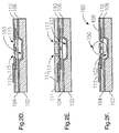
- Figs. 3A-3C are essentially the same as those shown in Figs. 2A-2C.
- the process deviates beginning in Fig. 3D, as a field passivation layer 110A is selectively removed in a desired pattern of the beam geometry.
- the field passivation layer 110A serves as a mask for a trench etch, i.e., a deep reactive ion etch (DRIE), that is utilized to form beam 152.
- a trench etch i.e., a deep reactive ion etch (DRIE)
- DRIE deep reactive ion etch
- the techniques described herein for minimizing a beam width of a sensing structure have broad applicability to sensing structures made through a variety of processes.
- the techniques may be employed on a silicon-on insulator (SOI) wafer that is modified through an SOI/deep trench process.
- SOI silicon-on insulator
- a primary difference between the processes is that the starting material would not initially have a buried cavity. That is, after forming the beam(s), the structure would be released by undercutting the insulating layer of the SOI wafer.
- Another alternative process would be to utilized a deep trench/undercut process to form the sensing structure.
- the starting material would be a plain wafer, e.g., a silicon wafer, and after a deep trench etch, the structure would be undercut using a lateral isotropic silicon etch.
- the techniques of the present invention may be used to minimize the beam width of a piezoresistive sensor.
- the passivation layer 110A may include, for example, a layer of thermal oxide, which is both a good field passivation and an effective mask for the DRIE. It should be appreciated that other films, common to integrated circuit (IC) processing, may also be utilized. As is shown in Fig. 3E, a photoresist layer 114A is applied and patterned to mask areas of the sensor away from the beam 152. Oversized windows are removed in the photoresist layer 114A in the beam 152 area to expose the field passivation layer 110A. The DRIE is then utilized in the process to remove the unmasked silicon from the wafer 104A, in the exposed areas defining the support beams and the inertial mass.
- a photoresist layer 114A is applied and patterned to mask areas of the sensor away from the beam 152. Oversized windows are removed in the photoresist layer 114A in the beam 152 area to expose the field passivation layer 110A.
- the DRIE is then utilized in the process to remove the unmasked silicon from the
- the requirement for the level-to-level alignment is eliminated.
- the space 'B' between the edge of the implant and the edge of the passivation layer (required to ensure junction isolation) and the width 'A' of the resistive implant are the limiting features of the design of sensor 170. This allows the sensor 170 to be reduced in overall size and cost. Furthermore, the sensor 170 can be manufactured using a number of existing process steps, without modification.
- the new sensor design is capable of providing a sensor having a twenty percent reduction in beam width.
- prior art accelerometers see Fig. 2G
- sensors constructed according to the present invention see Fig. 3G
- the new sensor design differs from the prior art sensor design in that the field passivation is used as a mask for a DRIE, which eliminates the need for level-to-level alignment, allowing for a reduction in width of the sensing beam(s).
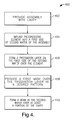
- an exemplary process 400 for producing the sensor 170 is depicted.
- an assembly is provided that includes a first wafer 102, having a cavity 103 formed into a first side of the first wafer 102, which is bonded to a second side of a second wafer 104A with an insulator layer 106.
- a piezoresistive layer 108 including at least one piezoresistive element, is then implanted, in step 404, into a first side of the second wafer 104A, which is opposite the second side of the second wafer 104A.
- a passivation layer 110A is formed on the first side of the second wafer 104A over the element.
- step 408 the passivation layer 110A is removed from selected areas on the first side of the second wafer 104A.
- a first mask is then provided on the passivation layer in a desired pattern.
- step 410 a beam 152, which includes the element, is then formed in the second wafer 104A over at least a portion of the cavity 103.
- the passivation layer 110A provides a second mask, in the formation of the beam 152, that determines a width of the formed beam 152.
Landscapes
- Engineering & Computer Science (AREA)
- Physics & Mathematics (AREA)
- General Physics & Mathematics (AREA)
- Manufacturing & Machinery (AREA)
- Microelectronics & Electronic Packaging (AREA)
- Pressure Sensors (AREA)
Applications Claiming Priority (1)
| Application Number | Priority Date | Filing Date | Title |
|---|---|---|---|
| US11/127,457 US7371601B2 (en) | 2005-05-12 | 2005-05-12 | Piezoresistive sensing structure |
Publications (3)
| Publication Number | Publication Date |
|---|---|
| EP1721865A2 true EP1721865A2 (fr) | 2006-11-15 |
| EP1721865A3 EP1721865A3 (fr) | 2011-09-28 |
| EP1721865B1 EP1721865B1 (fr) | 2012-12-26 |
Family
ID=36940606
Family Applications (1)
| Application Number | Title | Priority Date | Filing Date |
|---|---|---|---|
| EP06075963A Expired - Lifetime EP1721865B1 (fr) | 2005-05-12 | 2006-04-28 | Structure de capteur piézo-résistive |
Country Status (2)
| Country | Link |
|---|---|
| US (2) | US7371601B2 (fr) |
| EP (1) | EP1721865B1 (fr) |
Families Citing this family (4)
| Publication number | Priority date | Publication date | Assignee | Title |
|---|---|---|---|---|
| CN105174198A (zh) * | 2015-08-12 | 2015-12-23 | 中国电子科技集团公司第三十八研究所 | 一种封装结构的加速度传感器及其制备方法 |
| US10809139B2 (en) * | 2018-02-14 | 2020-10-20 | Carefusion 303, Inc. | Integrated sensor to monitor fluid delivery |
| JP7123652B2 (ja) * | 2018-06-20 | 2022-08-23 | 株式会社ディスコ | レーザー加工装置 |
| CN109678102B (zh) * | 2018-12-28 | 2024-07-19 | 杭州士兰集成电路有限公司 | Mems结构及其制造方法 |
Citations (1)
| Publication number | Priority date | Publication date | Assignee | Title |
|---|---|---|---|---|
| EP0899574A1 (fr) | 1997-02-21 | 1999-03-03 | Matsushita Electric Works, Ltd. | Element detecteur d'acceleration et son procede de production |
Family Cites Families (21)
| Publication number | Priority date | Publication date | Assignee | Title |
|---|---|---|---|---|
| US5177661A (en) * | 1989-01-13 | 1993-01-05 | Kopin Corporation | SOI diaphgram sensor |
| CN1027011C (zh) * | 1990-07-12 | 1994-12-14 | 涂相征 | 一种硅梁压阻加速度传感器及其制造方法 |
| US5199298A (en) * | 1991-06-21 | 1993-04-06 | Massachusetts Institute Of Technology | Wall shear stress sensor |
| JP2940293B2 (ja) * | 1992-03-31 | 1999-08-25 | 日産自動車株式会社 | 半導体加速度センサの製造方法 |
| US5323656A (en) * | 1992-05-12 | 1994-06-28 | The Foxboro Company | Overpressure-protected, polysilicon, capacitive differential pressure sensor and method of making the same |
| DE4309206C1 (de) * | 1993-03-22 | 1994-09-15 | Texas Instruments Deutschland | Halbleitervorrichtung mit einem Kraft- und/oder Beschleunigungssensor |
| US5427975A (en) * | 1993-05-10 | 1995-06-27 | Delco Electronics Corporation | Method of micromachining an integrated sensor on the surface of a silicon wafer |
| US5511428A (en) * | 1994-06-10 | 1996-04-30 | Massachusetts Institute Of Technology | Backside contact of sensor microstructures |
| US6316796B1 (en) * | 1995-05-24 | 2001-11-13 | Lucas Novasensor | Single crystal silicon sensor with high aspect ratio and curvilinear structures |
| US6012336A (en) * | 1995-09-06 | 2000-01-11 | Sandia Corporation | Capacitance pressure sensor |
| US5798283A (en) * | 1995-09-06 | 1998-08-25 | Sandia Corporation | Method for integrating microelectromechanical devices with electronic circuitry |
| US5772322A (en) * | 1996-05-31 | 1998-06-30 | Honeywell Inc. | Resonant microbeam temperature sensor |
| US5747705A (en) * | 1996-12-31 | 1998-05-05 | Honeywell Inc. | Method for making a thin film resonant microbeam absolute |
| US5808210A (en) * | 1996-12-31 | 1998-09-15 | Honeywell Inc. | Thin film resonant microbeam absolute pressure sensor |
| US6225140B1 (en) * | 1998-10-13 | 2001-05-01 | Institute Of Microelectronics | CMOS compatable surface machined pressure sensor and method of fabricating the same |
| US6953977B2 (en) * | 2000-02-08 | 2005-10-11 | Boston Microsystems, Inc. | Micromechanical piezoelectric device |
| US6511915B2 (en) * | 2001-03-26 | 2003-01-28 | Boston Microsystems, Inc. | Electrochemical etching process |
| US6757092B2 (en) * | 2001-12-10 | 2004-06-29 | Nayef M. Abu-Ageel | Micro-machine electrostatic actuator, method and system employing same, and fabrication methods thereof |
| US20030107794A1 (en) * | 2001-12-11 | 2003-06-12 | Siekkinen James W. | Micro mirror array |
| US20050172717A1 (en) * | 2004-02-06 | 2005-08-11 | General Electric Company | Micromechanical device with thinned cantilever structure and related methods |
| US20060037398A1 (en) * | 2004-08-19 | 2006-02-23 | Rich David B | Method for making an impact detector |
-
2005
- 2005-05-12 US US11/127,457 patent/US7371601B2/en not_active Expired - Lifetime
-
2006
- 2006-04-28 EP EP06075963A patent/EP1721865B1/fr not_active Expired - Lifetime
-
2008
- 2008-03-28 US US12/079,726 patent/US20080179698A1/en not_active Abandoned
Patent Citations (1)
| Publication number | Priority date | Publication date | Assignee | Title |
|---|---|---|---|---|
| EP0899574A1 (fr) | 1997-02-21 | 1999-03-03 | Matsushita Electric Works, Ltd. | Element detecteur d'acceleration et son procede de production |
Also Published As
| Publication number | Publication date |
|---|---|
| US7371601B2 (en) | 2008-05-13 |
| US20060258038A1 (en) | 2006-11-16 |
| EP1721865B1 (fr) | 2012-12-26 |
| US20080179698A1 (en) | 2008-07-31 |
| EP1721865A3 (fr) | 2011-09-28 |
Similar Documents
| Publication | Publication Date | Title |
|---|---|---|
| EP0762510B1 (fr) | Procédé de fabrication d'un dispositif monolithique semi-conducteur avec des structures micro-usinées en surface | |
| EP1920229B1 (fr) | Capteurs de pression et procedes de realisation | |
| JP5494861B2 (ja) | 半導体力学量センサの製造方法及び半導体力学量センサ | |
| US7259436B2 (en) | Micromechanical component and corresponding production method | |
| EP1808672A3 (fr) | Améliorations concernant le micro-usinage | |
| EP3030875B1 (fr) | Capteurs d'inertie et de pression sur monopuce | |
| EP3052901B1 (fr) | Capteurs inertiels et de pression sur une seule puce | |
| US20150276533A1 (en) | Low Pressure Sensor and Flow Sensor | |
| EP1096260B1 (fr) | Capteur micromécanique | |
| US6846724B2 (en) | Method for fabricating a microelectromechanical system (MEMS) device using a pre-patterned bridge | |
| EP1712515A2 (fr) | Technique pour réaliser des micro-structures électro-mécaniques | |
| EP3095754B1 (fr) | Capteur à basse pression et capteur d'écoulement | |
| US6469330B1 (en) | Process for manufacturing integrated devices comprising microstructures and associated suspended electrical interconnections | |
| US7170141B2 (en) | Method for monolithically integrating silicon carbide microelectromechanical devices with electronic circuitry | |
| US20080179698A1 (en) | Piezoresistive sensing structure | |
| JP2004505264A (ja) | 3軸センサ及びその製造方法 | |
| EP1770056B1 (fr) | Procédé pour réaliser une structure microélectromécanique | |
| JP4535547B2 (ja) | 残留応力を伴わない電気機械的超小型構造体を含む集積装置及びその製造方法 | |
| JP2004520177A (ja) | トンネリング・センサまたはスイッチ及びその製造方法 | |
| WO1993025915A1 (fr) | Procede de fabrication d'une puce monolithique contenant des circuits integres, et microstructure autoporteuse | |
| US10843921B2 (en) | Electrical connection to a micro electro-mechanical system | |
| JP3405222B2 (ja) | 半導体加速度センサ素子及びその製造方法 | |
| JPH09236615A (ja) | 力学量センサ、及び、力学量センサの製造方法 | |
| JP2008026240A (ja) | 半導体加速度センサ | |
| JP2009008456A (ja) | 半導体加速度センサ及びその製造方法 |
Legal Events
| Date | Code | Title | Description |
|---|---|---|---|
| PUAI | Public reference made under article 153(3) epc to a published international application that has entered the european phase |
Free format text: ORIGINAL CODE: 0009012 |
|
| AK | Designated contracting states |
Kind code of ref document: A2 Designated state(s): AT BE BG CH CY CZ DE DK EE ES FI FR GB GR HU IE IS IT LI LT LU LV MC NL PL PT RO SE SI SK TR |
|
| AX | Request for extension of the european patent |
Extension state: AL BA HR MK YU |
|
| REG | Reference to a national code |
Ref country code: DE Ref legal event code: R079 Ref document number: 602006033794 Country of ref document: DE Free format text: PREVIOUS MAIN CLASS: B81B0003000000 Ipc: B81C0001000000 |
|
| PUAL | Search report despatched |
Free format text: ORIGINAL CODE: 0009013 |
|
| AK | Designated contracting states |
Kind code of ref document: A3 Designated state(s): AT BE BG CH CY CZ DE DK EE ES FI FR GB GR HU IE IS IT LI LT LU LV MC NL PL PT RO SE SI SK TR |
|
| AX | Request for extension of the european patent |
Extension state: AL BA HR MK YU |
|
| RIC1 | Information provided on ipc code assigned before grant |
Ipc: G01P 15/12 20060101ALI20110819BHEP Ipc: B81C 1/00 20060101AFI20110819BHEP |
|
| 17P | Request for examination filed |
Effective date: 20120328 |
|
| 17Q | First examination report despatched |
Effective date: 20120423 |
|
| AKX | Designation fees paid |
Designated state(s): AT BE BG CH CY CZ DE DK EE ES FI FR GB GR HU IE IS IT LI LT LU LV MC NL PL PT RO SE SI SK TR |
|
| GRAP | Despatch of communication of intention to grant a patent |
Free format text: ORIGINAL CODE: EPIDOSNIGR1 |
|
| GRAS | Grant fee paid |
Free format text: ORIGINAL CODE: EPIDOSNIGR3 |
|
| GRAA | (expected) grant |
Free format text: ORIGINAL CODE: 0009210 |
|
| AK | Designated contracting states |
Kind code of ref document: B1 Designated state(s): AT BE BG CH CY CZ DE DK EE ES FI FR GB GR HU IE IS IT LI LT LU LV MC NL PL PT RO SE SI SK TR |
|
| REG | Reference to a national code |
Ref country code: GB Ref legal event code: FG4D |
|
| REG | Reference to a national code |
Ref country code: CH Ref legal event code: EP |
|
| REG | Reference to a national code |
Ref country code: AT Ref legal event code: REF Ref document number: 590340 Country of ref document: AT Kind code of ref document: T Effective date: 20130115 |
|
| REG | Reference to a national code |
Ref country code: DE Ref legal event code: R096 Ref document number: 602006033794 Country of ref document: DE Effective date: 20130307 |
|
| PG25 | Lapsed in a contracting state [announced via postgrant information from national office to epo] |
Ref country code: LT Free format text: LAPSE BECAUSE OF FAILURE TO SUBMIT A TRANSLATION OF THE DESCRIPTION OR TO PAY THE FEE WITHIN THE PRESCRIBED TIME-LIMIT Effective date: 20121226 Ref country code: FI Free format text: LAPSE BECAUSE OF FAILURE TO SUBMIT A TRANSLATION OF THE DESCRIPTION OR TO PAY THE FEE WITHIN THE PRESCRIBED TIME-LIMIT Effective date: 20121226 Ref country code: SE Free format text: LAPSE BECAUSE OF FAILURE TO SUBMIT A TRANSLATION OF THE DESCRIPTION OR TO PAY THE FEE WITHIN THE PRESCRIBED TIME-LIMIT Effective date: 20121226 |
|
| REG | Reference to a national code |
Ref country code: AT Ref legal event code: MK05 Ref document number: 590340 Country of ref document: AT Kind code of ref document: T Effective date: 20121226 |
|
| REG | Reference to a national code |
Ref country code: LT Ref legal event code: MG4D |
|
| REG | Reference to a national code |
Ref country code: NL Ref legal event code: VDEP Effective date: 20121226 |
|
| PG25 | Lapsed in a contracting state [announced via postgrant information from national office to epo] |
Ref country code: SI Free format text: LAPSE BECAUSE OF FAILURE TO SUBMIT A TRANSLATION OF THE DESCRIPTION OR TO PAY THE FEE WITHIN THE PRESCRIBED TIME-LIMIT Effective date: 20121226 Ref country code: LV Free format text: LAPSE BECAUSE OF FAILURE TO SUBMIT A TRANSLATION OF THE DESCRIPTION OR TO PAY THE FEE WITHIN THE PRESCRIBED TIME-LIMIT Effective date: 20121226 Ref country code: GR Free format text: LAPSE BECAUSE OF FAILURE TO SUBMIT A TRANSLATION OF THE DESCRIPTION OR TO PAY THE FEE WITHIN THE PRESCRIBED TIME-LIMIT Effective date: 20130327 |
|
| PG25 | Lapsed in a contracting state [announced via postgrant information from national office to epo] |
Ref country code: BG Free format text: LAPSE BECAUSE OF FAILURE TO SUBMIT A TRANSLATION OF THE DESCRIPTION OR TO PAY THE FEE WITHIN THE PRESCRIBED TIME-LIMIT Effective date: 20130326 Ref country code: AT Free format text: LAPSE BECAUSE OF FAILURE TO SUBMIT A TRANSLATION OF THE DESCRIPTION OR TO PAY THE FEE WITHIN THE PRESCRIBED TIME-LIMIT Effective date: 20121226 Ref country code: EE Free format text: LAPSE BECAUSE OF FAILURE TO SUBMIT A TRANSLATION OF THE DESCRIPTION OR TO PAY THE FEE WITHIN THE PRESCRIBED TIME-LIMIT Effective date: 20121226 Ref country code: SK Free format text: LAPSE BECAUSE OF FAILURE TO SUBMIT A TRANSLATION OF THE DESCRIPTION OR TO PAY THE FEE WITHIN THE PRESCRIBED TIME-LIMIT Effective date: 20121226 Ref country code: CY Free format text: LAPSE BECAUSE OF FAILURE TO SUBMIT A TRANSLATION OF THE DESCRIPTION OR TO PAY THE FEE WITHIN THE PRESCRIBED TIME-LIMIT Effective date: 20121226 Ref country code: BE Free format text: LAPSE BECAUSE OF FAILURE TO SUBMIT A TRANSLATION OF THE DESCRIPTION OR TO PAY THE FEE WITHIN THE PRESCRIBED TIME-LIMIT Effective date: 20121226 Ref country code: CZ Free format text: LAPSE BECAUSE OF FAILURE TO SUBMIT A TRANSLATION OF THE DESCRIPTION OR TO PAY THE FEE WITHIN THE PRESCRIBED TIME-LIMIT Effective date: 20121226 Ref country code: ES Free format text: LAPSE BECAUSE OF FAILURE TO SUBMIT A TRANSLATION OF THE DESCRIPTION OR TO PAY THE FEE WITHIN THE PRESCRIBED TIME-LIMIT Effective date: 20130406 Ref country code: IS Free format text: LAPSE BECAUSE OF FAILURE TO SUBMIT A TRANSLATION OF THE DESCRIPTION OR TO PAY THE FEE WITHIN THE PRESCRIBED TIME-LIMIT Effective date: 20130426 |
|
| PG25 | Lapsed in a contracting state [announced via postgrant information from national office to epo] |
Ref country code: NL Free format text: LAPSE BECAUSE OF FAILURE TO SUBMIT A TRANSLATION OF THE DESCRIPTION OR TO PAY THE FEE WITHIN THE PRESCRIBED TIME-LIMIT Effective date: 20121226 Ref country code: RO Free format text: LAPSE BECAUSE OF FAILURE TO SUBMIT A TRANSLATION OF THE DESCRIPTION OR TO PAY THE FEE WITHIN THE PRESCRIBED TIME-LIMIT Effective date: 20121226 Ref country code: PT Free format text: LAPSE BECAUSE OF FAILURE TO SUBMIT A TRANSLATION OF THE DESCRIPTION OR TO PAY THE FEE WITHIN THE PRESCRIBED TIME-LIMIT Effective date: 20130426 Ref country code: PL Free format text: LAPSE BECAUSE OF FAILURE TO SUBMIT A TRANSLATION OF THE DESCRIPTION OR TO PAY THE FEE WITHIN THE PRESCRIBED TIME-LIMIT Effective date: 20121226 |
|
| PG25 | Lapsed in a contracting state [announced via postgrant information from national office to epo] |
Ref country code: DK Free format text: LAPSE BECAUSE OF FAILURE TO SUBMIT A TRANSLATION OF THE DESCRIPTION OR TO PAY THE FEE WITHIN THE PRESCRIBED TIME-LIMIT Effective date: 20121226 |
|
| PLBE | No opposition filed within time limit |
Free format text: ORIGINAL CODE: 0009261 |
|
| STAA | Information on the status of an ep patent application or granted ep patent |
Free format text: STATUS: NO OPPOSITION FILED WITHIN TIME LIMIT |
|
| PG25 | Lapsed in a contracting state [announced via postgrant information from national office to epo] |
Ref country code: MC Free format text: LAPSE BECAUSE OF FAILURE TO SUBMIT A TRANSLATION OF THE DESCRIPTION OR TO PAY THE FEE WITHIN THE PRESCRIBED TIME-LIMIT Effective date: 20121226 |
|
| REG | Reference to a national code |
Ref country code: CH Ref legal event code: PL |
|
| 26N | No opposition filed |
Effective date: 20130927 |
|
| GBPC | Gb: european patent ceased through non-payment of renewal fee |
Effective date: 20130428 |
|
| PG25 | Lapsed in a contracting state [announced via postgrant information from national office to epo] |
Ref country code: IT Free format text: LAPSE BECAUSE OF FAILURE TO SUBMIT A TRANSLATION OF THE DESCRIPTION OR TO PAY THE FEE WITHIN THE PRESCRIBED TIME-LIMIT Effective date: 20121226 |
|
| REG | Reference to a national code |
Ref country code: DE Ref legal event code: R097 Ref document number: 602006033794 Country of ref document: DE Effective date: 20130927 |
|
| REG | Reference to a national code |
Ref country code: IE Ref legal event code: MM4A |
|
| PG25 | Lapsed in a contracting state [announced via postgrant information from national office to epo] |
Ref country code: CH Free format text: LAPSE BECAUSE OF NON-PAYMENT OF DUE FEES Effective date: 20130430 Ref country code: GB Free format text: LAPSE BECAUSE OF NON-PAYMENT OF DUE FEES Effective date: 20130428 Ref country code: LI Free format text: LAPSE BECAUSE OF NON-PAYMENT OF DUE FEES Effective date: 20130430 |
|
| REG | Reference to a national code |
Ref country code: FR Ref legal event code: ST Effective date: 20131231 |
|
| PG25 | Lapsed in a contracting state [announced via postgrant information from national office to epo] |
Ref country code: FR Free format text: LAPSE BECAUSE OF NON-PAYMENT OF DUE FEES Effective date: 20130430 |
|
| PG25 | Lapsed in a contracting state [announced via postgrant information from national office to epo] |
Ref country code: IE Free format text: LAPSE BECAUSE OF NON-PAYMENT OF DUE FEES Effective date: 20130428 |
|
| PG25 | Lapsed in a contracting state [announced via postgrant information from national office to epo] |
Ref country code: TR Free format text: LAPSE BECAUSE OF FAILURE TO SUBMIT A TRANSLATION OF THE DESCRIPTION OR TO PAY THE FEE WITHIN THE PRESCRIBED TIME-LIMIT Effective date: 20121226 |
|
| PG25 | Lapsed in a contracting state [announced via postgrant information from national office to epo] |
Ref country code: HU Free format text: LAPSE BECAUSE OF FAILURE TO SUBMIT A TRANSLATION OF THE DESCRIPTION OR TO PAY THE FEE WITHIN THE PRESCRIBED TIME-LIMIT; INVALID AB INITIO Effective date: 20060428 Ref country code: LU Free format text: LAPSE BECAUSE OF NON-PAYMENT OF DUE FEES Effective date: 20130428 |
|
| REG | Reference to a national code |
Ref country code: DE Ref legal event code: R081 Ref document number: 602006033794 Country of ref document: DE Owner name: DELPHI TECHNOLOGIES IP LIMITED, BB Free format text: FORMER OWNER: DELPHI TECHNOLOGIES, INC., TROY, MICH., US |
|
| P01 | Opt-out of the competence of the unified patent court (upc) registered |
Effective date: 20230327 |
|
| PGFP | Annual fee paid to national office [announced via postgrant information from national office to epo] |
Ref country code: DE Payment date: 20250317 Year of fee payment: 20 |