EP1722404A2 - Alliage metallique à faible travail d'extraction - Google Patents
Alliage metallique à faible travail d'extraction Download PDFInfo
- Publication number
- EP1722404A2 EP1722404A2 EP06113814A EP06113814A EP1722404A2 EP 1722404 A2 EP1722404 A2 EP 1722404A2 EP 06113814 A EP06113814 A EP 06113814A EP 06113814 A EP06113814 A EP 06113814A EP 1722404 A2 EP1722404 A2 EP 1722404A2
- Authority
- EP
- European Patent Office
- Prior art keywords
- metal
- gate electrode
- lanthanide
- layer
- semiconductor
- Prior art date
- Legal status (The legal status is an assumption and is not a legal conclusion. Google has not performed a legal analysis and makes no representation as to the accuracy of the status listed.)
- Ceased
Links
Images






Classifications
-
- H—ELECTRICITY
- H10—SEMICONDUCTOR DEVICES; ELECTRIC SOLID-STATE DEVICES NOT OTHERWISE PROVIDED FOR
- H10P—GENERIC PROCESSES OR APPARATUS FOR THE MANUFACTURE OR TREATMENT OF DEVICES COVERED BY CLASS H10
- H10P30/00—Ion implantation into wafers, substrates or parts of devices
- H10P30/20—Ion implantation into wafers, substrates or parts of devices into semiconductor materials, e.g. for doping
- H10P30/202—Ion implantation into wafers, substrates or parts of devices into semiconductor materials, e.g. for doping characterised by the semiconductor materials
- H10P30/204—Ion implantation into wafers, substrates or parts of devices into semiconductor materials, e.g. for doping characterised by the semiconductor materials into Group IV semiconductors
-
- H—ELECTRICITY
- H10—SEMICONDUCTOR DEVICES; ELECTRIC SOLID-STATE DEVICES NOT OTHERWISE PROVIDED FOR
- H10D—INORGANIC ELECTRIC SEMICONDUCTOR DEVICES
- H10D64/00—Electrodes of devices having potential barriers
- H10D64/01—Manufacture or treatment
- H10D64/013—Manufacture or treatment of electrodes having a conductor capacitively coupled to a semiconductor by an insulator
- H10D64/01302—Manufacture or treatment of electrodes having a conductor capacitively coupled to a semiconductor by an insulator the insulator being formed after the semiconductor body, the semiconductor being silicon
- H10D64/01304—Manufacture or treatment of electrodes having a conductor capacitively coupled to a semiconductor by an insulator the insulator being formed after the semiconductor body, the semiconductor being silicon characterised by the conductor
- H10D64/01306—Manufacture or treatment of electrodes having a conductor capacitively coupled to a semiconductor by an insulator the insulator being formed after the semiconductor body, the semiconductor being silicon characterised by the conductor the conductor comprising a layer of silicon contacting the insulator, e.g. polysilicon
- H10D64/01308—Manufacture or treatment of electrodes having a conductor capacitively coupled to a semiconductor by an insulator the insulator being formed after the semiconductor body, the semiconductor being silicon characterised by the conductor the conductor comprising a layer of silicon contacting the insulator, e.g. polysilicon the conductor further comprising a non-elemental silicon additional conductive layer, e.g. a metal silicide layer formed by the reaction of silicon with an implanted metal
- H10D64/0131—Manufacture or treatment of electrodes having a conductor capacitively coupled to a semiconductor by an insulator the insulator being formed after the semiconductor body, the semiconductor being silicon characterised by the conductor the conductor comprising a layer of silicon contacting the insulator, e.g. polysilicon the conductor further comprising a non-elemental silicon additional conductive layer, e.g. a metal silicide layer formed by the reaction of silicon with an implanted metal the additional conductive layer comprising a silicide layer formed by the silicidation reaction between the layer of silicon with a metal layer which is not formed by metal implantation
-
- H—ELECTRICITY
- H10—SEMICONDUCTOR DEVICES; ELECTRIC SOLID-STATE DEVICES NOT OTHERWISE PROVIDED FOR
- H10D—INORGANIC ELECTRIC SEMICONDUCTOR DEVICES
- H10D64/00—Electrodes of devices having potential barriers
- H10D64/01—Manufacture or treatment
- H10D64/013—Manufacture or treatment of electrodes having a conductor capacitively coupled to a semiconductor by an insulator
- H10D64/01302—Manufacture or treatment of electrodes having a conductor capacitively coupled to a semiconductor by an insulator the insulator being formed after the semiconductor body, the semiconductor being silicon
- H10D64/01304—Manufacture or treatment of electrodes having a conductor capacitively coupled to a semiconductor by an insulator the insulator being formed after the semiconductor body, the semiconductor being silicon characterised by the conductor
- H10D64/01318—Manufacture or treatment of electrodes having a conductor capacitively coupled to a semiconductor by an insulator the insulator being formed after the semiconductor body, the semiconductor being silicon characterised by the conductor the conductor comprising a layer of alloy material, compound material or organic material contacting the insulator, e.g. TiN
- H10D64/0132—Manufacture or treatment of electrodes having a conductor capacitively coupled to a semiconductor by an insulator the insulator being formed after the semiconductor body, the semiconductor being silicon characterised by the conductor the conductor comprising a layer of alloy material, compound material or organic material contacting the insulator, e.g. TiN the conductor being a metallic silicide
-
- H—ELECTRICITY
- H10—SEMICONDUCTOR DEVICES; ELECTRIC SOLID-STATE DEVICES NOT OTHERWISE PROVIDED FOR
- H10D—INORGANIC ELECTRIC SEMICONDUCTOR DEVICES
- H10D64/00—Electrodes of devices having potential barriers
- H10D64/60—Electrodes characterised by their materials
- H10D64/66—Electrodes having a conductor capacitively coupled to a semiconductor by an insulator, e.g. MIS electrodes
- H10D64/667—Electrodes having a conductor capacitively coupled to a semiconductor by an insulator, e.g. MIS electrodes the conductor comprising a layer of alloy material, compound material or organic material contacting the insulator, e.g. TiN workfunction layers
- H10D64/668—Electrodes having a conductor capacitively coupled to a semiconductor by an insulator, e.g. MIS electrodes the conductor comprising a layer of alloy material, compound material or organic material contacting the insulator, e.g. TiN workfunction layers the layer being a silicide, e.g. TiSi2
-
- H—ELECTRICITY
- H10—SEMICONDUCTOR DEVICES; ELECTRIC SOLID-STATE DEVICES NOT OTHERWISE PROVIDED FOR
- H10P—GENERIC PROCESSES OR APPARATUS FOR THE MANUFACTURE OR TREATMENT OF DEVICES COVERED BY CLASS H10
- H10P30/00—Ion implantation into wafers, substrates or parts of devices
- H10P30/20—Ion implantation into wafers, substrates or parts of devices into semiconductor materials, e.g. for doping
- H10P30/208—Ion implantation into wafers, substrates or parts of devices into semiconductor materials, e.g. for doping of electrically inactive species
-
- H—ELECTRICITY
- H10—SEMICONDUCTOR DEVICES; ELECTRIC SOLID-STATE DEVICES NOT OTHERWISE PROVIDED FOR
- H10D—INORGANIC ELECTRIC SEMICONDUCTOR DEVICES
- H10D30/00—Field-effect transistors [FET]
- H10D30/60—Insulated-gate field-effect transistors [IGFET]
- H10D30/62—Fin field-effect transistors [FinFET]
-
- H—ELECTRICITY
- H10—SEMICONDUCTOR DEVICES; ELECTRIC SOLID-STATE DEVICES NOT OTHERWISE PROVIDED FOR
- H10D—INORGANIC ELECTRIC SEMICONDUCTOR DEVICES
- H10D64/00—Electrodes of devices having potential barriers
- H10D64/60—Electrodes characterised by their materials
- H10D64/66—Electrodes having a conductor capacitively coupled to a semiconductor by an insulator, e.g. MIS electrodes
- H10D64/68—Electrodes having a conductor capacitively coupled to a semiconductor by an insulator, e.g. MIS electrodes characterised by the insulator, e.g. by the gate insulator
- H10D64/691—Electrodes having a conductor capacitively coupled to a semiconductor by an insulator, e.g. MIS electrodes characterised by the insulator, e.g. by the gate insulator comprising metallic compounds, e.g. metal oxides or metal silicates
Definitions
- the present invention relates to the field of semiconductor devices, in particular to field effect devices comprising a metal gate electrode, more particularly a metal gate electrode formed by silicidation of a semiconductor material and to methods for fabricating such field effect devices.
- the well known polysilicon is being replaced as gate electrode material by metals.
- Such metal gates do not suffer from the shortcomings of a semiconducting gate electrode such as gate depletion, dopant diffusion or medium range resistance.
- obtaining the desired work function for both nMOS and pMOS devices in view of controlling the threshold voltage is not as straightforward as in the case of polysilicon gates as the work function of polysilicon can be tuned by doping the polysilicon with a well-defined amount of an appropriate dopant, e.g. Boron for pMOS devices thereby forming a high work function gate electrode and Phosphorus for nMOS devices thereby forming a low work function gate electrode.
- an appropriate dopant e.g. Boron for pMOS devices thereby forming a high work function gate electrode and Phosphorus for nMOS devices thereby forming a low work function gate electrode.
- Midgap metals are materials having a Fermi level near the midgap position between the valence and conduction band of the semiconducting substrate on which the MOSFET is formed.
- An example of such midgap metal is CoSi 2 having a work function of about 4.65eV.
- This metal gate material is formed by a full silicidation (FUSI) of a polysilicon gate electrode whereby essentially all the polysilicon is converted into a silicide during reaction with Co.
- FUSI full silicidation
- nMOS and pMOS devices can be obtained using such a midgap metal, these threshold voltages are too high compared with the supply voltage at which these nMOS and pMOS are to operate.
- the material of the gate electrode of the nMOS device is a metal having a low work function, ideally about 4 to 4.2eV
- the material of the pMOS gate electrode is another metal having a high work function, ideally about 5 to 5.2eV.
- Finding an appropriate low-work function metal for use as nMOS gate electrode is of particular importance as such metal reacts rapidly with the oxygen present in the underlying dielectric, e.g. silicon-oxide or high-k dielectrics.
- Tuning of the work function of a gate electrode metal by alloying it with other metals, in order to match the work function requirements for a nMOS or pMOS gate electrode is known.
- Mistra et al discloses in published United States application US 2003/0160227 the alloying of a first metal having a higher work function with a second metal B having a lower work function. Depending on the ratio, the resulting alloy A x B 1-x will have a work function ranging from the work function of the first metal A to the work function of the second metal B. The lowest work function obtainable is determined by the work function of the second metal B, which is selected from the group of Mn, Mg, V, Ti, Cr, Y, Zr, Ta, La, Gd, Sm, Pr, Nb, Al, Hf and alloys thereof. Mistra et al. does not teach the formation of a fully silicided gate electrode using such binary alloys.
- J. Liu et al discloses in "Dual-Work-Function Metal Gates by Full Silicidation of Poly-Si With Co-Ni Bilayers", IEEE electron device letters 2005 , the formation of dual-work-function metal gates fabricated by full silicidation (FUSI) of a Co-Ni bi-layer and a comparison of these alloyed metal gates with single-metal FUSI systems of CoSi 2 and NiSi.
- the alloy of CO x Ni 1-x Si allows combining the low work function of NiSi with the thermal stability of CoSi.
- Yu et al discloses in "Low Work function Fully Silicided Gate on SiO2/Si and La AlO3/GOI n-MOSFETS", proceedings of 62nd Device Research Conference (DRC), pp. 21, Notre Dame, Indiana, June, 2004 , the combination of the low resistive NiSi, having a high work function, of about 4.9eV with Hf or TiSi to obtain a low work function of 4.2eV and 4.3eV respectively.
- the present invention aims at providing a new low work function material, which is stable, reproducible, and methods for producing said new low work function material, which are reproducible and easy to implement.
- the present invention relates to a method for modulating the work function of a silicided gate electrode.
- the present invention relates to the use of at least one lanthanide, preferably the use of Yb, for reducing the work function of a fully or partially silicided gate electrode.
- a method of the invention comprises the steps of:
- said semiconductor layer comprises (or consists of) Si, Ge or SiGe.
- said step of implanting lanthanide(s) ions can be performed after the silicidation step.
- said step of implanting lanthanide(s) ions can be performed between the step of depositing said metal and the silicidation step.
- said semiconductor layer is formed upon a high-k (i.e. k > 3,9) dielectric layer.
- two, three or more lanthanides can be used.
- said at least one lanthanide is Yb.
- Said metal can be any metal suitable for silicidation.
- Ni is used for silicidation.
- the step of siliciding said semiconductor material can comprise the step of providing a thermal budget such as to convert substantially all said semiconductor material into silicide and optionally the step of removing any unreacted metal.
- the step of siliciding said semiconductor material can comprise the step of providing a first thermal budget to convert partially said semiconductor material into silicide, the step of removing any unreacted metal, and the step of providing a second thermal budget for completion of the conversion of said semiconductor material into silicide.
- Another aspect of the invention relates to a metallic alloy comprising at least one lanthanide (preferably Yb), a suitable metal for silicidation (preferably Ni), and a semiconductor preferably selected from the group consisting of Silicon (Si), Germanium (Ge) and silicon-germanium (SiGe).
- a metallic alloy comprising at least one lanthanide (preferably Yb), a suitable metal for silicidation (preferably Ni), and a semiconductor preferably selected from the group consisting of Silicon (Si), Germanium (Ge) and silicon-germanium (SiGe).
- a metallic alloy according to the invention can be used as a low work function material (i.e. smaller than about 4,5eV, preferably smaller than about 4.2eV, more particularly between about 4 and about 4,2eV).
- a method for forming a low work function metallic alloy can comprise the steps of:
- the invention also relates to a nMOSFET comprising a gate electrode and a gate dielectric, wherein the gate electrode comprises (or consists of) at least one lanthanide, a suitable metal for silicidation, and a semiconductor preferably selected from the group consisting of Silicon (Si), Germanium (Ge) and silicon-germanium (SiGe).
- the gate electrode comprises (or consists of) at least one lanthanide, a suitable metal for silicidation, and a semiconductor preferably selected from the group consisting of Silicon (Si), Germanium (Ge) and silicon-germanium (SiGe).
- the gate electrode consists of an alloy of said at least one lanthanide, said suitable metal, and said semiconductor.
- said at least one lanthanide is Ytterbium (Yb).
- said metal is nickel (Ni).
- said semiconductor is Si.
- the gate electrode consists of an alloy of Yb, Ni and Si.
- a method for forming a nMOSFET can comprise the steps of:
- the step of depositing said metal and said lanthanide(s) can consist of depositing alternatively at least one layer of metal and at least one layer of said lanthanide(s).
- the last layer deposited can be said metal layer.
- Said metal and said lanthanide (s) can be sequentially sputtered on said semiconductor gate electrode.
- said metal and said lanthanide(s) can be co-deposited, in particular can be simultaneously sputtered on said semiconductor gate electrode.
- a method for forming a nMOSFET according to the invention can further comprise the step of forming a capping layer over said deposited metal and lanthanide(s) before the step of transforming said semiconductor gate electrode in a silicided gate electrode.
- a method for forming a nMOSFET according to the invention can further comprise the step of selectively removing the unreacted metal and lanthanide(s) after forming the silicided gate electrode.
- said semiconductor layer is formed upon a high-k dielectric layer.
- said at least one lanthanide is Yb.
- the metal used for silicidation is Ni.
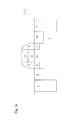
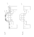
- Figure 1 shows a schematic cross-section of devices according to the present invention (a) bulk MOSFET, (b) MuGFET.
- Figure 2 a-g show schematic cross-sections of a device according to the present invention illustrating different steps in the manufacturing process.
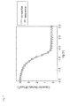
- Figure 3 shows measured and simulated capacitance C versus gate voltage V g data for a capacitor with FUSI gate according to the present invention.
- Figure 4 shows measured (lines) and simulated (symbols) capacitance C versus gate voltage V g data for a capacitor with FUSI gate according to the present invention (solid squares) and for a capacitor with a prior art Nickel-silicide FUSI gate (circles).
- FIG. 5 shows Equivalent Oxide Thickness (EOT) vs. Flat-band voltage V fb data for capacitors with a FUSI gate electrode according to the present invention.
- Figure 6 shows measured (lines) and simulated (symbols) capacitance C versus gate voltage V g data for capacitors with a FUSI gate according to the present invention, whereby the Nickel/Ytterbium ratio in the as-deposited layer was varied from one capacitor to another.
- Figure 7 shows measured (lines) and simulated (symbols) capacitance C versus gate voltage V g data for capacitors with a FUSI gate according to the present invention, whereby Nickel and Ytterbium was either co-deposited (circles) or sequentially deposited (diamond).
- Figure 8 a-b shows schematic cross-sections of a precursor device illustrating a method according to the present invention for reducing the work function of a metal gate.
- Figure 9a and 9b show flat-band voltage (V) versus EOT data for a As, P or Sb implanted NiSi FUSI gate respectively on SiO 2 and HfSiON dielectric gate.
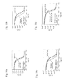
- Figure 10 shows capacitance C versus gate voltage V g data, wherein the work function could be modulated to n-type by ion implantation of Yb into respectively (a) NiSi FUSI gate on SiON dielectric, (b) Ni 2 Si FUSI gate on SiON dielectric, (c) NiSi FUSI gate on HfSiON dielectric, (d) Ni 2 (SiGe) FUSI gate on HfSiON dielectric.
- the present invention provides a low work function metallic alloy comprising (or consisting of) at least one lanthanide, a suitable metal for silicidation, and a semiconductor, said semiconductor comprising Si, Ge or SiGe.
- the lanthanides consist of 15 elements from lanthanum to lutetium on the periodic table, including lanthanum (La), cerium (Ce), praseodymium (Pr), neodymium (Nd), promethium (Pm), samarium (Sm), europium (Eu), gadolinium (Gd), terbium (Tb), dysprosium (Dy), holmium (Ho), erbium (Er), thulium (Tm), ytterbium (Yb) and lutetium (Lu).
- La lanthanum
- Ce cerium
- Pr praseodymium
- Nd neodymium
- promethium Pm
- Sm samarium
- Eu europium
- Gd gadolinium
- Tb terbium
- Dy dysprosium
- Ho holmium
- Er erbium
- Tm thulium
- Yb yt
- said lanthanide is Yb.
- said metal is Ni.
- said semiconductor is Si.
- a preferred metallic alloy of the invention consists of Yb, Ni and Si.
- the present invention also discloses a method to manufacture a metallic alloy of the invention.
- the method comprises the steps of:
- the present invention discloses a nMOSFET comprising a gate electrode (5) and a gate dielectric (4) characterized in that the gate electrode (5) comprises at least one lanthanide, a suitable metal for silicidation, and a semiconductor, said semiconductor comprising Si, Ge or SiGe.
- the present invention also discloses a method to manufacture a fully silicided nMOSFET (FUSI nMOSFET), comprising the steps of:
- the method can further comprise forming a capping layer (15) over said layer stack (14) before forming the silicided gate electrode (5).
- the method can further comprise selectively removing the unreacted metal after forming the silicided gate electrode (5).
- silica can refer to the reaction between a metal and silicon, but is not intended to be limited to silicon.
- the reaction of a metal with Ge, or any other suitable semiconductor material may still be referred to as silicidation.
- metal-rich silicide refers to the material resulting from the reaction between said metal and said semiconductor, wherein the ratio metal-to-semiconductor is larger than 1.
- the present invention provides a nMOSFET device comprising a gate electrode and a gate dielectric characterized in that the gate electrode comprises Nickel (Ni), Ytterbium (Yb) and Silicon (Si).
- the gate electrode comprises or consists of an alloy of Nickel (Ni), Ytterbium (Yb) and Silicon (Si).
- Said alloy can be represented by the formula Ni x Yb y Si 1-x-y where 0.3 ⁇ x ⁇ 0.7, and 0.005 ⁇ y ⁇ 0.2.
- a metallic alloy comprising (or consisting of) Nickel (Ni), Ytterbium (Yb) and Silicon (Si).
- Said metallic alloy can be represented by the formula Ni x Yb y Si 1-x-y where 0.3 ⁇ x ⁇ 0.7, and 0.005 ⁇ y ⁇ 0.2.
- Said metallic alloy can be used as a low work function material.
- Said metallic alloy can be used as a low work function material in a nMOSFET device, i.e. said work function is smaller than (about) 4,5 eV, preferably said work function is comprised between (about) 3,9 eV and (about) 4,5 eV, more preferably said work function is comprised between (about) 4 eV and (about) 4,2 eV.
- the present invention also provides a method for forming an alloy, which can be used as low work function material, comprising the steps of:
- the present invention also provides a method for forming a (partially or fully) silicided nMOSFET comprising the steps of:
- a fully silicided nMOSFET (FUSI nMOSFET) is formed.
- the step of depositing said Nickel and Ytterbium can consist of depositing alternatively at least one layer of nickel and at least one layer of ytterbium.
- Said Nickel and Ytterbium can be sequentially sputtered on said semiconductor gate electrode.
- the last layer deposited is a nickel layer.
- said Nickel and Ytterbium can be co-deposited, in particular they can be simultaneously sputtered on said semiconductor gate electrode.
- a capping layer can be deposited over said deposited Nickel and Ytterbium before the step of transforming said semiconductor gate electrode in a Nickel-Ytterbium-Silicide gate electrode.
- a method of the invention can further comprise the step of selectively removing the unreacted Nickel and Ytterbium after forming the Nickel-Ytterbium Silicide gate electrode.
- the present invention relates to the use of at least one lanthanide for reducing the work function of a gate electrode.
- a method for modulating the work function of a silicided gate electrode comprising the steps of:
- the step of implanting lanthanide(s) ions can be performed between the step of depositing said metal and the silicidation step.
- the step of implanting lanthanide(s) ions can be performed after the silicidation step.
- an annealing step is performed after the step of implanting the lanthanide(s) ions.
- the silicidation step is such as to obtain a fully silicided gate electrode.
- the step of fully siliciding said semiconductor material can comprise the step of providing a thermal budget to convert substantially all said semiconductor material into silicide and the step of removing any unreacted metal.
- the step of fully siliciding said semiconductor material can comprise the step of providing a first thermal budget to convert partially said semiconductor material into silicide, the step of removing any unreacted metal, and the step of providing a second thermal budget for completion of the conversion of said semiconductor material into silicide.
- this optimized 2-step RTP process can be used for FUSI gates (more particularly Ni x Si y FUSI gates) to achieve uniform phase control at different gate lengths.
- the gate dielectric layer can be a layer of electrically insulating material, such as SiO 2 , SiN, or SiON, formed by any suitable method, such as chemical vapor deposition (CVD).
- CVD chemical vapor deposition
- the gate dielectric is a layer a high-k dielectric material, such as HfSiON.
- the gate electrode (before silicidation) is advantageously formed from a polysilicon layer deposited on the gate dielectric.
- the gate electrode is advantageously deposited by a chemical vapor decomposition (CVD) method, followed by patterning and etching.
- CVD chemical vapor decomposition
- the spacers are formed from an insulating material such as silicon dioxide (SiO 2 ), silicon nitride (SiN), or silicon oxynitride (SiON).
- the spacers are advantageously deposited and patterned by any art recognized method, such as CVD followed by anisotropic etching.
- the metal layer advantageously comprises Ni atoms.
- the use of other metals is possible within the scope of the present invention.
- Co, Ti, and Pt are other suitable metals for forming silicides.
- the metal layer can be deposited by any method known in the art.
- the advantages of a method according to the invention using lanthanide(s) ions implantation over implantation with other species currently used are that it is more effective in reducing the effective work function of metal gates, in particular of metal gates on high-k dielectrics such as HfSiON, and of preventing adhesion or peeling problems.
- the introduction of said lanthanide(s), more particularly Yb, by ion implantation is more advantageous than the deposition of a layer of said lanthanide(s).
- One advantage is an easier implementation into CMOS flows for which the lanthanide(s) (more particularly Yb) is/are only desired in the NMOS devices.
- lanthanide(s) co-deposition (more particularly Yb) this would mean the need for two separate deposition steps on NMOS and PMOS.
- Another advantage is that a much lower amount of lanthanide(s) is used, making the process much more similar to the pure metal silicidation (e.g. Ni silicidation).
- Another advantage is the higher efficiency with which the lanthanide(s) is/are segregated to the dielectric interface, making the method using ion implantation according to the invention more efficient to reduce the work function (i.e. same work function reduction for much less total amount of Yb for example).
- the lanthanide used is Yb, implanted into a polySi layer.
- the metal used is Ni, to obtain a fully silicided gate.
- the silicide phase is preferably NiSi, but any Ni-rich silicide is also contemplated (such as Ni 2 Si, etc).
- energies in the 40-60 keV range and doses of 2E15 to 6e15 can be used.
- the implanted Si can be annealed before metal deposition for silicidation.
- anneal could be a spike or soak activation anneal at temperatures in the 900-1100°C range for example.
- the step of full silicidation of the gate can thus be performed.
- Figures 1a and 1b show a schematic cross-sectional view of n-type Metal-Oxide-Semiconductor Field Effect Transistors (nMOSFET) according to the invention.
- nMOSFET n-type Metal-Oxide-Semiconductor Field Effect Transistors
- a nMOS device of the invention comprises a gate stack formed on a semiconducting layer (2).
- the gate stack comprises a gate dielectric (4) in contact with this semiconducting layer (2) and a gate electrode (5) in contact with this gate dielectric (4).
- the gate dielectric can be a silicon-oxide, a silicon-oxy-nitride (Si x O y N 1-x-y ), an high-k dielectric (i.e. k>3,9) such as Hafnium or Aluminum silicates or oxides, e.g. HfO 2 , Al 2 O 3 .
- the gate electrode (5) comprises a low work function metallic alloy.
- This low work function metallic alloy comprises one, two or more of the lanthanides, a suitable metal for silicidation and a semiconductor comprising (or consisting of) Si, Ge or SiGe.
- a preferred low work function metallic alloy of the invention comprises (or consists of) Nickel, Ytterbium and silicon.
- the nMOS device can further comprise spacers (8) formed adjacent the gate stack (4, 5) and junction regions (6, 7, 9, 10).
- Figure 1a shows an example of a nMOSFET device formed on a bulk substrate 2 while figure 1b shows a MugFET nMOS, i.e. a Multiple gate FET such as a FinFET, formed upon the dielectric (12) of a SOI substrate.
- MugFET nMOS i.e. a Multiple gate FET such as a FinFET
- Figure 2 illustrates by means of schematic cross-sections a process for manufacturing devices according to the present invention.
- a bulk nMOSFET is used (represented) although the invention is not intended to be limited thereto.
- Figure 2a shows a cross-section of the nMOSFET after the spacers (8) after formed.
- a method of the invention can comprise the steps of forming a gate stack (4, 13), and spacers (8) adjacent this gate stack.
- Spacers can be formed from silicon-oxide, silicon-oxy-nitride (Si x O y N 1-x-y ), silicon nitride, silicon carbide or from a combination of these materials.
- n-type source/drain junction regions are formed, typically as a combination of extension regions (6,7) underneath the spacers (8) and connection regions (9, 10) adjacent these extension regions and aligned to the spacers (8).
- a channel region (11) is present in the semiconductor layer, which in this case is the semiconductor substrate itself (2).
- the active area region (not indicated) in which the transistor (1) is formed is separated from other active area regions by so-called field regions (3) formed by known techniques such as Local Oxidation of Silicon (LOCOS) or Shallow Trench Insulation (STI).
- LOCOS Local Oxidation of Silicon
- STI Shallow Trench Insulation
- the gate dielectric (4) can be a silicon-oxide, a silicon-oxy-nitride (Si x O y N 1-x-y ), an high-k dielectric such as Hafnium or Aluminum silicates or oxides, e.g. HfO 2 , Al 2 O 3 .
- the gate electrode (13) is formed in a semiconductor material.
- This semiconductor material is preferably silicon. This silicon can be in a monocrystalline, polycrystalline or amorphous state.
- the thickness of the gate electrode (13), i.e. the amount of semiconductor material available, can be determined in view of the desired composition of the later-formed silicide as will be shown later.
- a diffusion barrier layer (17) can be present in between the gate electrode (13) and the gate dielectric (4).
- This diffusion barrier (17) will prevent diffusion of the lanthanide, more particularly of Ytterbium, into the gate dielectric (4) during the silicidation process.
- An example of such diffusion barrier (17) is silicon-nitride.
- the layer stack (14) can be in the form of single layer comprising an alloy having the desired composition, i.e. the ratio lanthanide(s)/metal (e.g. the ratio Nickel/Ytterbium), and the desired total amount of lanthanide(s) and metal (e.g. Nickel and Ytterbium), i.e. layer thickness.
- the desired composition i.e. the ratio lanthanide(s)/metal (e.g. the ratio Nickel/Ytterbium), and the desired total amount of lanthanide(s) and metal (e.g. Nickel and Ytterbium), i.e. layer thickness.
- This single layer can be obtained for example by simultaneously sputtering said lanthanide(s) and metal (e.g. Nickel and Ytterbium) from their respective targets on the substrate at predetermined deposition rates or by sputtering an alloy of lanthanide(s) and metal (e.g. Nickel Ytterbium) having the desired composition on the substrate.
- metal e.g. Nickel and Ytterbium
- the layer stack (14) can be in the form of a stack of layers e.g. by sequentially sputtering layers of respectively lanthanide(s) and metal (e.g. Nickel and Ytterbium) whereby the thickness of the individual layers determines the amount of lanthanide(s) and metal (e.g. Nickel and Ytterbium) available and the ratio of the layer thickness determines the ratio of lanthanide(s)/metal (e.g. Nickel/Ytterbium ratio).
- metal e.g. Nickel and Ytterbium
- a capping layer (15) is deposited on the layer stack (14) as shown in figure 2d.
- This capping layer prevents oxidation of the lanthanide(s) (e.g. Ytterbium) during the subsequent silicide forming annealing process.
- the material of this capping layer must have oxygen diffusion barrier properties and be substantially oxide free.
- this capping layer comprises HfN.
- the layer stack (14) can be formed by sequentially sputtering layers of lanthanide(s) and metal (e.g. first depositing Ytterbium and covering the deposited Ytterbium layer with Nickel), whereby the top layer (e.g. Ni) can act as an oxygen diffusion barrier (15) and no additional capping layer is needed.
- metal e.g. first depositing Ytterbium and covering the deposited Ytterbium layer with Nickel
- lanthanide(s) and metal can be co-deposited or an alloy of lanthanide(s) and metal (e. g. Nickel and Ytterbium) can be sputtered, and a metal layer (e.g. Nickel layer) can be used as capping layer thereby avoiding the need for a separate capping layer (15) and corresponding etching steps to remove such additional capping layer.
- the silicidation process is performed.
- metal e.g. Nickel and Ytterbium
- Nickel, Ytterbium from the layer stack (14) and silicon from the gate electrode (13) react with each other to form a metallic Nickel-Ytterbium silicide.
- the semiconductor gate electrode (13) is transformed in a metallic silicided gate electrode (e.g. into a Nickel Ytterbium Silicon gate electrode) (5).
- composition of this alloy depends on the relative amounts available of lanthanide(s), metal and semiconductor (e.g. Nickel, Ytterbium and silicon).
- the conditions of this silicidation process e.g. time, temperature of this annealing process, are chosen such that substantially the complete semiconductor gate electrode (13) is converted into a metallic gate electrode (5) resulting in a so-called Fully Silicided gate electrode (FUSI).
- the silicide forming temperature is within the range of 350°C to 600°C, more preferably at about 400°C while the duration of the silicide forming process is within the range of 30s to 90s, preferably about 60s.
- the unreacted metals e.g. Nickel, Ytterbium
- the silicide (16) the spacers (8) and the field regions (3).
- the selective removal is performed by a wet etch of about 5 minutes using an etchant comprising HNO 3 .
- this capping layer is preferably selectively removed before removing the unreacted metals.
- HfN is used to form the capping layer
- a wet etch using an etchant such as diluted HF is used to selectively remove the HfN capping layer.
- Figure 2e shows the device comprising the FUSI gate electrode (5) after selectively removing the unreacted lanthanide(s) and metal (e.g. Nickel and Ytterbium) and the capping layer if present.
- metal e.g. Nickel and Ytterbium
- MOS capacitors are fabricated by first depositing a SiON dielectric layer (4) thereon.
- a layer stack (14) of Ytterbium (Yb) (14a) and Nickel (Ni) (14b) are deposited, preferably by Plasma Vapor Depositing (VPD) in an Argon ambient.
- VPD Plasma Vapor Depositing
- Both Ni and Yb can be co-sputtered and then the deposition of Yb can be stopped while the deposition of Ni is continued.
- HfN Hafnium Nitride
- the silicide forming process is preferably performed in vacuum (10e-5 torr, i.e. 1,33.10e-5 mbar) at about 400°C for about 1 minute.
- the HfN capping layer is selectively removed, preferably by a wet etch, e.g. of about 5 minutes, e.g. using diluted HF solution.
- the remaining unreacted metal, Ni and/or Yb is selectively removed, preferably by a wet etch, e.g. of about 5 minutes, e.g. using dilute HNO 3 .
- MOS capacitors are obtained having a FUSI Nickel-Ytterbium-Silicide gate electrode (5) on top of a SiON gate dielectric (4) formed on p-type substrates (2), as depicted in figure 2g.
- Nickel-Ytterbium-Silicide represented by the formula Ni x Yb y Si 1-x-y
- x is equal to 0.55
- y is equal to 0.12.
- Figure 3 shows the measured and simulated C (fF/ ⁇ m 2 )-V g (V) data for a 100 by 100 ⁇ m 2 capacitor processed as described in the example section.
- the flatband voltage V fb is extracted to be about -0.8V.
- the complete silicidation of the polysicilicon layer is confirmed by comparing the extracted Equivalent Oxide Thickness (EOT) value of 3.75nm with the physical thickness of the dielectrics determined by ellipsometry. From this comparison one can conclude that no depletion effect occurs at the gate electrode side and that gate capacitance measured during the positive bias of the gate electrode with respect to substrate corresponds the capacitance of the gate dielectric.
- EOT Equivalent Oxide Thickness
- Figure 4 compares the measured and simulated (solid line) C (fF/ ⁇ m 2 )-V g (V) data for a 100 by 100 ⁇ m 2 capacitor having a Nickel-Ytterbium-Silicon FUSI gate (solid squares) with the measured and simulated C (fF/ ⁇ m 2 )-V g (V) data for a similar, 100 by 100 ⁇ m 2 , capacitor but having a prior art Nickel-Silicide (NiSi) FUSI gate (open circles). Due to the presence of the Nickel-Ytterbium-Silicon FUSI gate the C-V g curve is shifted about 500mV towards more negative gate voltages. This voltage shifts illustrates that the low work function metal according to the present invention exhibits n-type electronic properties and that it is suitable as electrode material for nMOS devices.
- capacitor structures were processed which are similar to the capacitor structures disclosed in the example section.
- the composition of the Nickel Ytterbium Silicon FUSI gate was varied and several approaches to form the as-deposited Nickel Ytterbium metal stack were used.
- Nickel-Ytterbium metal stacks were deposited having substantially the same as-deposited stack thickness of about 80nm but with different Nickel/Ytterbium thickness ratio.
- the thickness of the Nickel and of the Ytterbium layer is controlled by the rate and time at which Nickel, respectively, Ytterbium are co-sputtered.
- Figure 6 shows the effect of the Nickel Ytterbium Silicon composition on the C-V characteristics of these structures.
- the equivalent oxide thickness of these capacitor structures is determined as being about 7.9nm.
- the C-V curve is shifted to negative gate voltages from a Ni/Yb thickness ratio as low as 40/1 having a flat-band voltage V fb of - 0.71V (solid squares).
- Ni/Yb 21/4 (open circles) with V fb of -0.81V
- Ni/Yb 3/1 (upward diamond) with V fb of -0.89V.
- Nickel Ytterbium metal stacks were deposited having substantially the same as-deposited stack thickness of about 80nm and substantially the same Nickel/Ytterbium thickness ratio of 4/1.
- the Nickel Ytterbium metal stack (14) was formed either by simultaneous depositing the Nickel and Ytterbium as was done in the example section or by sequentially depositing both metals, e.g. first depositing the Ytterbium layer and afterwards forming the Nickel layer.
- the equivalent oxide thickness of these capacitor structures is determined as being about 7.9nm.
- Figure 7 shows the effect of the deposition method on the C-V characteristics of these structures.
- Nickel and Ytterbium are deposited in a sequential way (open diamonds) the corresponding C-V curve coincides with the C-V curve obtained for the co-sputtered metal stack (open circles) and a flat-band voltage of about -0.81V is obtained.
- FIG. 8a shows a precursor nMOS device (1) in which Yb ions are implanted into a gate electrode (13) comprising silicon.
- This gate electrode can further comprise nickel.
- the gate electrode is a nickel silicide.
- the implanted gate electrode (5) is converted into a nickel-ytterbium-silicide by using thermal processing resulting in the device illustrated by figure 8b.
- Figure 9 shows the flatband voltage of an nMOS transistor as function of the equivalent oxide thickness for a nickel silicide/silicon oxide gate stack (a) or for a nickel silicide/hafnium silicon oxide gate stack (b).
- FIG. 9a, 9b contains on inset showing the capacitance-voltage curves from which the flatband voltages are extracted.
- the flatband voltage for various doping conditions of the gate electrode are shown: undoped or respectively Boron, Arsenic, Phosphorous doped.
- Figure 10a-b shows the capacitance voltage curves for Yb doped fully nickel silicided gate electrode (5) formed on a silicon oxide nitride dielectric layer (4) (figure 10a, 10b) or on a hafnium silicon oxide nitride dielectric layer (4) (figure 10c, 10d).
- the nickel silicide can be a Ni 0.5 Si 0.5 (figure 10a, 10c) or Ni 2 Si 1 (figure 10b, 10d). In every figure a comparison is made with undoped nickel silicide counterpart and the difference in workfunction between the Yb doped and undoped nickel silicide is given at the bottom of each figure.
- the present invention hence discloses a low work function metal comprising at least one lanthanide, a metal and a semiconductor, more particularly comprising Nickel, Ytterbium and Silicon.
- This low work function metal can be used as n-type gate electrode material, for example to form the gate electrode of a nMOSFET.
- the present invention allows the formation of electronic circuits comprising nMOSFETs and pMOSFETs, wherein the gate electrode of the nMOSFETs is formed according to the present invention.
- MOS capacitors were fabricated by first depositing a SiON dielectric layer (4) thereon.
- SiON layers with various thicknesses have been formed on various wafers.
- the polysilicon layer (13) had a thickness of about 100nm.
- a layer stack (14) of Ytterbium (Yb) (14a) and Nickel (Ni) (14b) was deposited by Plasma Vapor Depositing (VPD) in an Argon ambient.
- VPD Plasma Vapor Depositing
- Yb was deposited at a rate of about 10nm/min, and Ni at a rate of about 17nm/min.
- both Ni and Yb were co-sputtered for 1.5 min. Then the deposition of Yb was stopped while the deposition of Ni was continued for another 2.5 min.
- HfN Hafnium Nitride
- the silicide forming process was performed in vacuum (10e-5 torr, i.e. 1,33.10e-5 mbar) at about 400°C for about 1min.
- the HfN capping layer was selectively removed by a wet etch of about 5 minutes using diluted HF solution. Then the remaining unreacted metal, Ni and/or Yb, was selectively removed by a wet etch of about 5 minutes using dilute HNO 3 .
- MOS capacitors are obtained having a FUSI Nickel-Ytterbium-Silicon gate electrode (5) on top of a SiON gate dielectric (4) formed on p-type substrates (2), as depicted in figure 2g.
- the resulting Nickel-Ytterbium-Silicon gate electrode layer had a thickness of about 110 to 120nm with a smooth interface with the underlying SiON gate dielectric.
- the average sheet resistance R s of this gate electrode layer (5) was about 5.5 ohm/square which is comparable to the sheet resistance of a NickelSilicon gate electrode layer.
- AES Auger - Electron-Spectroscopy
- the present invention can also be described as a method for modulating the work function of a silicided gate electrode comprising:
- step (a) comprises (or consists of):
- Said step of depositing said metal and said lanthanide(s) can consist of depositing alternatively at least one layer of metal and at least one layer of lanthanide(s).
- the last layer deposited in said alternating sequence is a metal layer.
- said metal and said lanthanide(s) layers can be deposited using sputtering.
- said metal and said lanthanide(s) can be co-deposited, and more particularly can be simultaneously sputtered.
- a method for modulating the work function of a silicided gate electrode according to the invention can further comprise the step of forming a capping layer over said deposited metal and lanthanide(s), before the step of transforming said layer in a silicided gate electrode.
- a method for modulating the work function of a silicided gate electrode according to the invention can further comprise the step of selectively removing the unreacted metal and lanthanide(s), after forming the silicided gate electrode.
- said at least one lanthanide is provided by ions implantation into the surface of said semiconductor material.
- step (a) comprises:
- a method for modulating the work function of a silicided gate electrode according to the invention can comprise the steps of:
- an annealing step is performed after said implanting step.
- said silicidation step (transforming said different layers into a silicided gate electrode) can comprise:
- said silicidation step can comprise:
- said gate dielectric is preferably a high-k (i.e. k > 3,9) dielectric layer.
- said (at least one) lanthanide is Yb.
- said metal is Ni.
- a method for modulating the work function of a silicided gate electrode according to the invention can be used for the manufacture of a fully silicided nMOSFET (FUSI nMOSFET).
Landscapes
- Electrodes Of Semiconductors (AREA)
- Thin Film Transistor (AREA)
- Insulated Gate Type Field-Effect Transistor (AREA)
Priority Applications (1)
| Application Number | Priority Date | Filing Date | Title |
|---|---|---|---|
| EP06113814A EP1722404A3 (fr) | 2005-05-11 | 2006-05-11 | Alliage metallique à faible travail d'extraction |
Applications Claiming Priority (4)
| Application Number | Priority Date | Filing Date | Title |
|---|---|---|---|
| US68027605P | 2005-05-11 | 2005-05-11 | |
| EP05447278A EP1796151A1 (fr) | 2005-12-09 | 2005-12-09 | Alliage métallique a faible travail d'extraction |
| EP06447002 | 2006-01-06 | ||
| EP06113814A EP1722404A3 (fr) | 2005-05-11 | 2006-05-11 | Alliage metallique à faible travail d'extraction |
Publications (2)
| Publication Number | Publication Date |
|---|---|
| EP1722404A2 true EP1722404A2 (fr) | 2006-11-15 |
| EP1722404A3 EP1722404A3 (fr) | 2007-08-15 |
Family
ID=39855175
Family Applications (1)
| Application Number | Title | Priority Date | Filing Date |
|---|---|---|---|
| EP06113814A Ceased EP1722404A3 (fr) | 2005-05-11 | 2006-05-11 | Alliage metallique à faible travail d'extraction |
Country Status (2)
| Country | Link |
|---|---|
| EP (1) | EP1722404A3 (fr) |
| JP (1) | JP2008226862A (fr) |
Cited By (1)
| Publication number | Priority date | Publication date | Assignee | Title |
|---|---|---|---|---|
| EP1916706A3 (fr) * | 2006-10-23 | 2009-05-27 | Interuniversitair Microelektronica Centrum (IMEC) | Procédé pour la formation d'un dispositif semiconducteur et dispositif semiconducteur ainsi obtenu |
Families Citing this family (1)
| Publication number | Priority date | Publication date | Assignee | Title |
|---|---|---|---|---|
| JP2007067225A (ja) * | 2005-08-31 | 2007-03-15 | Toshiba Corp | 半導体装置およびその製造方法 |
Citations (2)
| Publication number | Priority date | Publication date | Assignee | Title |
|---|---|---|---|---|
| WO2005029583A2 (fr) * | 2003-09-19 | 2005-03-31 | Spinnaker Semiconductor, Inc. | Circuit integre a barriere de schottky |
| US20050093033A1 (en) | 2003-09-05 | 2005-05-05 | Atsuhiro Kinoshita | Field effect transistor and manufacturing method thereof |
Family Cites Families (3)
| Publication number | Priority date | Publication date | Assignee | Title |
|---|---|---|---|---|
| US4738937A (en) * | 1985-10-22 | 1988-04-19 | Hughes Aircraft Company | Method of making ohmic contact structure |
| US6303479B1 (en) * | 1999-12-16 | 2001-10-16 | Spinnaker Semiconductor, Inc. | Method of manufacturing a short-channel FET with Schottky-barrier source and drain contacts |
| US7384868B2 (en) * | 2003-09-15 | 2008-06-10 | International Business Machines Corporation | Reduction of silicide formation temperature on SiGe containing substrates |
-
2006
- 2006-05-11 JP JP2006132386A patent/JP2008226862A/ja active Pending
- 2006-05-11 EP EP06113814A patent/EP1722404A3/fr not_active Ceased
Patent Citations (2)
| Publication number | Priority date | Publication date | Assignee | Title |
|---|---|---|---|---|
| US20050093033A1 (en) | 2003-09-05 | 2005-05-05 | Atsuhiro Kinoshita | Field effect transistor and manufacturing method thereof |
| WO2005029583A2 (fr) * | 2003-09-19 | 2005-03-31 | Spinnaker Semiconductor, Inc. | Circuit integre a barriere de schottky |
Cited By (2)
| Publication number | Priority date | Publication date | Assignee | Title |
|---|---|---|---|---|
| EP1916706A3 (fr) * | 2006-10-23 | 2009-05-27 | Interuniversitair Microelektronica Centrum (IMEC) | Procédé pour la formation d'un dispositif semiconducteur et dispositif semiconducteur ainsi obtenu |
| US7759748B2 (en) | 2006-10-23 | 2010-07-20 | Imec | Semiconductor device with reduced diffusion of workfunction modulating element |
Also Published As
| Publication number | Publication date |
|---|---|
| EP1722404A3 (fr) | 2007-08-15 |
| JP2008226862A (ja) | 2008-09-25 |
Similar Documents
| Publication | Publication Date | Title |
|---|---|---|
| US7504329B2 (en) | Method of forming a Yb-doped Ni full silicidation low work function gate electrode for n-MOSFET | |
| CN100477224C (zh) | 半导体结构及其制造方法 | |
| JP5336857B2 (ja) | 金属不純物の導入による導電性電極の仕事関数を変更する方法(およびその半導体構造体) | |
| US8409943B2 (en) | Work function adjustment with the implant of lanthanides | |
| CN101345260B (zh) | 半导体结构 | |
| WO2008098890A1 (fr) | Grilles métalliques à faible piégeage de charge et des caractéristiques de fiabilité diélectriques améliorées pour des empilements diélectriques de grille à haute constante diélectrique | |
| US6809394B1 (en) | Dual metal-alloy nitride gate electrodes | |
| JP5157450B2 (ja) | 半導体装置およびその製造方法 | |
| US7605077B2 (en) | Dual metal integration scheme based on full silicidation of the gate electrode | |
| US20090057786A1 (en) | Semiconductor device and method of manufacturing semiconductor device | |
| EP1796151A1 (fr) | Alliage métallique a faible travail d'extraction | |
| US20090134469A1 (en) | Method of manufacturing a semiconductor device with dual fully silicided gate | |
| EP1722404A2 (fr) | Alliage metallique à faible travail d'extraction | |
| US8344460B2 (en) | Method for forming a nickelsilicide FUSI gate | |
| US7786537B2 (en) | Semiconductor device and method for manufacturing same | |
| US7781319B2 (en) | Method of manufacturing semiconductor device | |
| US7776673B2 (en) | Method of manufacturing semiconductor device | |
| JPWO2006129637A1 (ja) | 半導体装置 | |
| JP2006032712A (ja) | 半導体装置及びその製造方法 |
Legal Events
| Date | Code | Title | Description |
|---|---|---|---|
| PUAI | Public reference made under article 153(3) epc to a published international application that has entered the european phase |
Free format text: ORIGINAL CODE: 0009012 |
|
| AK | Designated contracting states |
Kind code of ref document: A2 Designated state(s): AT BE BG CH CY CZ DE DK EE ES FI FR GB GR HU IE IS IT LI LT LU LV MC NL PL PT RO SE SI SK TR |
|
| AX | Request for extension of the european patent |
Extension state: AL BA HR MK YU |
|
| PUAL | Search report despatched |
Free format text: ORIGINAL CODE: 0009013 |
|
| AK | Designated contracting states |
Kind code of ref document: A3 Designated state(s): AT BE BG CH CY CZ DE DK EE ES FI FR GB GR HU IE IS IT LI LT LU LV MC NL PL PT RO SE SI SK TR |
|
| AX | Request for extension of the european patent |
Extension state: AL BA HR MK YU |
|
| 17P | Request for examination filed |
Effective date: 20080214 |
|
| 17Q | First examination report despatched |
Effective date: 20080317 |
|
| AKX | Designation fees paid |
Designated state(s): AT BE BG CH CY CZ DE DK EE ES FI FR GB GR HU IE IS IT LI LT LU LV MC NL PL PT RO SE SI SK TR |
|
| RAP1 | Party data changed (applicant data changed or rights of an application transferred) |
Owner name: TEXAS INSTRUMENTS INCORPORATED Owner name: NATIONAL UNIVERSITY OF SINGAPORE Owner name: IMEC |
|
| RAP1 | Party data changed (applicant data changed or rights of an application transferred) |
Owner name: TEXAS INSTRUMENTS INCORPORATED Owner name: INTERUNIVERSITAIR MICROELEKTRONICA CENTRUM (IMEC) |
|
| STAA | Information on the status of an ep patent application or granted ep patent |
Free format text: STATUS: THE APPLICATION HAS BEEN REFUSED |
|
| 18R | Application refused |
Effective date: 20120406 |