EP1724645A1 - Voltmètre pour contrôler l'uniformité de la charge d'un photorécepteur - Google Patents
Voltmètre pour contrôler l'uniformité de la charge d'un photorécepteur Download PDFInfo
- Publication number
- EP1724645A1 EP1724645A1 EP06113907A EP06113907A EP1724645A1 EP 1724645 A1 EP1724645 A1 EP 1724645A1 EP 06113907 A EP06113907 A EP 06113907A EP 06113907 A EP06113907 A EP 06113907A EP 1724645 A1 EP1724645 A1 EP 1724645A1
- Authority
- EP
- European Patent Office
- Prior art keywords
- charge
- photoreceptor
- uniformity
- scanner
- intensity
- Prior art date
- Legal status (The legal status is an assumption and is not a legal conclusion. Google has not performed a legal analysis and makes no representation as to the accuracy of the status listed.)
- Granted
Links
Images


Classifications
-
- G—PHYSICS
- G03—PHOTOGRAPHY; CINEMATOGRAPHY; ANALOGOUS TECHNIQUES USING WAVES OTHER THAN OPTICAL WAVES; ELECTROGRAPHY; HOLOGRAPHY
- G03G—ELECTROGRAPHY; ELECTROPHOTOGRAPHY; MAGNETOGRAPHY
- G03G15/00—Apparatus for electrographic processes using a charge pattern
- G03G15/50—Machine control of apparatus for electrographic processes using a charge pattern, e.g. regulating differents parts of the machine, multimode copiers, microprocessor control
- G03G15/5033—Machine control of apparatus for electrographic processes using a charge pattern, e.g. regulating differents parts of the machine, multimode copiers, microprocessor control by measuring the photoconductor characteristics, e.g. temperature, or the characteristics of an image on the photoconductor
- G03G15/5037—Machine control of apparatus for electrographic processes using a charge pattern, e.g. regulating differents parts of the machine, multimode copiers, microprocessor control by measuring the photoconductor characteristics, e.g. temperature, or the characteristics of an image on the photoconductor the characteristics being an electrical parameter, e.g. voltage
Definitions
- the present disclosure relates to effectrastatagraphic printing and/or xerography systems. Specifically this disclosure relates to in-situ machine measurement of photoreceptor charging uniformity in marking engines within xerographic systems.
- a photoreceptor may be supported by a mechanical carrier, such as a drum or a belt.
- the photoreceptor may be charged to a generally uniform charge by subjecting the photoreceptor to a suitable charging device.
- the charge distribution on the photoreceptor may then be altered by the application of radiation, e.g., a laser, to the surface of the photoreceptor.
- the toner particles adhere electrostatically to the suitably charged portions of the photoreceptor.
- the toner particles may then be transferred, by the application of electric charge to a print sheet or intermediate belt, forming the desired image on the print sheet or intermediate belt.
- An electric charge may also be used to separate or "detack" the print sheet from the photoreceptor.
- the charge uniformity of the photoreceptor bears a direct relationship on the quality of the work product of the xerographic system.
- Control systems for uniform charge distribution requires monitoring the charge disposed on the photoreceptor and has been made possible by advances in non-contacting electrostatic voltmeters (ESV's) which measure the surface voltage of the photoreceptor.
- ESV's electrostatic voltmeters
- MEM micro-electro-mechanical
- An area of ongoing research and development is in reducing the overall size of electrostatographic system components towards the goal of an economical and capacity-extendible all-in-one process cartridge for easy adaptive use in a family of compact electrostatographic reproduction machines having different volume capacities and consumable life cycles. Furthermore, multiple smaller tandem marking engines may be advantageously used in parallel engines to increase machine throughput.
- an electrostatic printing apparatus comprises:
- Exemplary embodiments of disclosed herein apparatus and methods to provide cross-process charge uniformity information take advantage of the small footprint and reduced packaging of MEMS based ESV devices to enable mounting of ESV devices in locations and configurations previously unavailable.
- An exemplary embodiment of a cross-process charge uniformity scanner may comprise mounting an ESV on the sliding portion of an automatic charge cleaner in a xerographic device.
- the cleaning device may incorporate a lead screw or similar method known in the art to traverse the cleaning pads or brushes from one end of the photoreceptor to the other in a direction transverse to the fast scanning direction of the light radiation device. Attaching the ESV to the portion of the cleaner that moves across the process may allow surface voltage data to be recorded for the entire process while in motion, thereby acquiring a assessment of uniformity scan.
- Another exemplary embodiment of a cross-process charge uniformity scanner may take advantage of the small size of MEMS based ESV devices to incorporate a plurality of ESV devices disposed at spaced apart locations along the length of the photoreceptor in an axis transverse to a slow scanning direction of the photoreceptor.
- exemplary embodiments of MEMS ESV devices incorporated in a xerographic device may allow the xerographic device to assess charge uniformity and ensure color consistency across multiple imaging devices in tightly integrated parallel printing architectures.
- xerographic devices such as illustrated in Fig. 1, and is particularly directed to apparatus and methods to perform in-situ xerographic device measurement of photoreceptor charge uniformity and may be used to automatically change defined subsystem and system settings to try to restore charging uniformity.
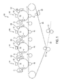
- Fig. 1 illustrates elements of an electrostatographic and/or xerographic color marking engine 100, such as a copier or a "laser printer.”
- the marking engine 100 may include four tandem process cartridges 102-108, each providing one of three primary colors, typically cyan, magenta and yellow, and in addition, optionally black.
- Each process cartridge 102-108 may function similarly. As such, only the operation of a single process cartridge is discussed as representative of all four process cartridges.
- Each process cartridge may comprise a photoreceptor 110, which although shown in Figs. 1-3 as a drum 110, may be in the form of a belt or other photoreceptive transfer medium.
- the photoreceptor 110 may define a charge-retentive surface for forming electrostatic images thereon.
- the photoreceptor 110 may be rotated in a process direction P.
- the first step in the process may be an initial charging of a relevant surface of the photoreceptor 110.
- This initial charging may be performed by a charge device 112 that imparts an electrostatic charge on the surface of the photoreceptor 110 rotating past the charge device 112.
- a charge uniformity scanner 128 may then assess the uniformity of the applied charge by measuring the surface charge on the photoreceptor 110 in at least one location along the length of the photoreceptor 110. Based on the assessment of the charge uniformity, several options are available to try to restore charging uniformity, trigger a critical replacement unit (CRU) which may include a charge device 112 replacement, or setting a warning flag.
- CRU critical replacement unit
- the charged portions of the photoreceptor 110 may then be selectively discharged in a configuration corresponding to a desired image to be printed, for example, by a raster output scanner (ROS), not shown, which generally comprises a laser source and a rotatable mirror which act together, in a manner known in the art, to discharge certain areas of the surface of photoreceptor 110 according to the desired image to be printed.
- ROS raster output scanner
- a laser may be used to selectively discharge the surface of the photoreceptor 110
- other apparatus that may be used for this purpose may include an LED bar, or, in a copier, a light-lens system.
- the laser source may be modulated (turned on and off) in accordance with digital image data fed thereto, and the rotating mirror may cause the modulated beam from laser source to move in a fast-scan direction perpendicular to the process direction P of the photoreceptor 110.
- the remaining charged areas may be developed by a developer unit 114, for example, causing a supply of dry toner to contact or otherwise approach the surface of photoreceptor 110.
- the developed image may then be advanced, by the motion of photoreceptor 110, to a bias transfer roller, or transfer station 116, for example, causing the toner adhering to the photoreceptor 110 to be electrically transferred to a common intermediate transfer belt 118. Any residual toner remaining on the photoreceptor 110 may be removed by a cleaning blade 120 or equivalent device.
- the complete color image may be transferred at transfer station 122 to a medium, such as a sheet of plain paper 126, to form the image thereon.
- a medium such as a sheet of plain paper 126
- Belt cleaner 128 may clean the transfer belt 118 of any residual toner.
- the sheet of plain paper 126, with the toner image thereon, may then be passed through a fuser 124, for example, causing the toner to melt, or fuse, into the sheet of paper 126.
- color process cartridges shown in Fig. 1 may operate within a tandem color marking engine, corresponding elements may operate in other color marking engines including a single photoreceptor with multiple exposure and development devices, as well as in monochrome printers including a single photoreceptor and a single exposure and development device.
- the photoreceptor 110 and uniformity scanner 128 may be configured as part of a cartridge that is readily removable and replaceable, relative to a larger printing apparatus.
- Such removable cartridges may further include a supply of marking material and/or a fusing mechanism.
- MEMS micro-electro-mechanical systems
- ESV electrostatic voltmeter
- xerographic devices such as illustrated in Fig. 1 as well as MEMS based ESV devices.
- MEMS based ESV devices MEMS based ESV devices.
- the principles and techniques described herein may be used in conjunction with other ESV devices and in other photoreceptor configurations and methods.
- These configurations and methods may include, for example, color as well as monochrome printers, photoreceptor drum as well as belt supported systems, raster output scanner (ROS) systems as well as electrostatographic devices utilizing direct writing techniques such as full width array (FWA) LED imaging.
- ROS raster output scanner
- Figure 2 is an exemplary embodiment illustrating subassemblies of a marker engine 102 and charge uniformity scanner 128, and may include a processor assembly 202 in communication with a charge device 112 and a charge uniformity scanner interface unit 206, through cables 218 and 220 respectively.
- the processor assembly 202 may control operation of a number of other subassemblies including the cleaning assembly 120 as well as the developer unit 114, alternate embodiments of the xerographic device 100 may comprise distributed processors including a separate processor to control the operation of the charge uniformity scanner 128.
- the charge uniformity scanner 128, of Fig. 1 may further comprise an ESV device 204 slideably mounted so as to measure charge intensity on the surface 212 of the photoreceptor 110 as the ESV device 204 traverses the length of the photoreceptor 110 in a fast scanning direction 201.
- the method by which the ESV device 204 may be caused to traverse the length of the photoreceptor 110 may take advantage of elements already disposed in the xerographic device 100.
- Charge device cleaning assemblies 120 are used to clean toner or other contamination from the corona generating portions of the charge device 112 and may include a drive mechanism, such as a motor and screw drive to advance the cleaning pads or brushes in a fast scanning direction 201.
- the ESV device 204 may likewise be slideably mounted to a screw drive 216 driven by motor 214, connected by a cable 222 to the processor assembly 202, so as to measure a charge deposited along the length of the photoreceptor 110 as the ESV device 204 is advanced in a fast scanning direction 201.
- the processor assembly 202 may initiate a uniformity assessment scan of the photoreceptor 110 whereby the screw drive 216 is rotated, causing the ESV device 204 to traverses the length of the photoreceptor 110, while measuring charge intensity at a plurality of locations on the surface 212 of the photoreceptor 110.
- the measured charge intensity at the plurality of locations may then be transmitted to an interface unit 206 through cable 208.
- Cable 208 may be of sufficient length and flexibility so as to allow the ESV device 204 to freely traverse back and forth across the length of the photoreceptor 110.
- the output signal of the ESV device 204 may be a digital signal which is received by the interface unit 206 and is then made available to the processor assembly 202.
- the ESV device 204 may provide an analog signal output which may be converted to a digital signal by an A/D converter (not shown) within the interface unit 206.
- A/D converters are known to those of ordinary skill in the art and the specific implementation of the A/D converter is non-limiting. Regardless of whether the output of the ESV device 204 is analog or digital, a plurality of measured voltage readings at spaced apart intervals on the surface of the photoreceptor serve as input to the processor assembly 202 which determines the charge uniformity of the photoreceptor 112.
- Fig. 3 illustrates an alternate exemplary embodiment of a charge uniformity scanner 128 of Fig. 1, comprising an interface unit 312 receiving input from a plurality of spaced apart ESV devices 304-310, each ESV device presenting a waterfront footprint of approximately 3-6 mm at pre-determined locations along the length of the photoreceptor 110.
- the exemplary embodiment illustrated in Fig. 3 may be advantageous in certain applications where it may not be feasible, desirable or cost effective to implement a single moveable ESV device. Such applications may include, for example, electrostatographic devices not having an automatic cleaning device having a drive mechanism, or where the unit price of an ESV device may justify multiple ESV devices.
- the processor assembly 302 assesses charge uniformity based upon a plurality of voltage measurements.
- the plurality of voltage measurements are obtained from a plurality of spaced apart ESV devices 304-310.
- the output of each of the ESV devices 304-310 are wired 314 to the interface unit 312 and under processor control may be gated through an analog gate and A/D converter within interface unit 312 to selectively output a measured voltage from each of the ESV devices 304-310 to the processor assembly 302.
- an alternate exemplary embodiment may locate the analog gate, the A/D converter and the rest of the logic contained within the interface unit 312 into the processor assembly 302.
- the physical location of components required to perform the charge uniformity diagnostic functions described herein is based upon manufacturing analysis and is non-limiting.
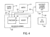
- Figure 4 illustrates an exemplary functional block diagram of the voltage uniformity scanner embodiment as shown in Fig. 2.
- the processor assembly 202 may control the uniformity scanner 128, the charge device 112, the cleaning assembly 120 as well as the developer unit 114.
- the processor assembly 202 may include a processor 402, a memory 404 accessible to the processor 402, and control leads to other subassemblies including the charge device 112 and the drive mechanism 212.
- Program instruction code stored in the memory 404 may configure the processor 402 to control the operation of the charge uniformity scanner 128, the charge device 112 and the drive mechanism 212 based on an assessed charge uniformity of the photoreceptor 110.
- the program instruction code may direct the processor 402 to assess charge uniformity based upon a plurality of spaced apart measurements of the photoreceptor 110 taken by the ESV device 204.
- Charge uniformity may, for example, be determined as the statistical mean of spaced apart voltage measurements. Low uniformity as well as other calculations, which may include deviations from the mean at specific locations, may trigger automatic attempts to restore uniformity and/or to initiate diagnostics and CRU replacement.
- the implementation of the processor 402 and memory 404 is non-limiting, and the program instruction code implementing the functionality of the charge uniformity scanner 128 may be incorporated within an alternative memory device or may be accessed by an alternate processor within the xerographic device 100.
- An exemplary implementation of the charge uniformity scanner 128 may include a uniformity scan performed during apparatus setup, apparatus power-ups, or at predetermined intervals during long run jobs.
- the program instruction code may be configured to: activate the drive mechanism 212 to cause the ESV device 202 to traverse the length of the photoconductor measuring voltage levels at spaced apart intervals; assess charge uniformity based upon the plurality of measurements; and based upon the assessed charge, the control processor 204 may further attempt to restore charge uniformity by one or more of: controlling the intensity of the applied charge and/or adjust dishcarge levels applied by the light radiation device; direct automatic cleaning of the charge device 112; and setting a maintenance flag and/or generate a maintenance report or message, indicating the need for a customer replacement unit (CRU) replacement.
- CRU customer replacement unit
- FIG. 3 A block diagram illustrating the uniformity scanner embodied in Fig. 3 would replace the single ESV device with a plurality of ESV devices and would not include control logic/programming to activate a drive mechanism.
Landscapes
- Engineering & Computer Science (AREA)
- Microelectronics & Electronic Packaging (AREA)
- Physics & Mathematics (AREA)
- General Physics & Mathematics (AREA)
- Control Or Security For Electrophotography (AREA)
- Cleaning In Electrography (AREA)
- Electrostatic Charge, Transfer And Separation In Electrography (AREA)
Applications Claiming Priority (1)
| Application Number | Priority Date | Filing Date | Title |
|---|---|---|---|
| US11/133,196 US7324766B2 (en) | 2005-05-20 | 2005-05-20 | Cross-process charge uniformity scanner |
Publications (2)
| Publication Number | Publication Date |
|---|---|
| EP1724645A1 true EP1724645A1 (fr) | 2006-11-22 |
| EP1724645B1 EP1724645B1 (fr) | 2009-08-05 |
Family
ID=36481224
Family Applications (1)
| Application Number | Title | Priority Date | Filing Date |
|---|---|---|---|
| EP06113907A Expired - Lifetime EP1724645B1 (fr) | 2005-05-20 | 2006-05-15 | Voltmètre pour contrôler l'uniformité de la charge d'un photorécepteur |
Country Status (4)
| Country | Link |
|---|---|
| US (1) | US7324766B2 (fr) |
| EP (1) | EP1724645B1 (fr) |
| JP (1) | JP2006330722A (fr) |
| DE (1) | DE602006008213D1 (fr) |
Cited By (1)
| Publication number | Priority date | Publication date | Assignee | Title |
|---|---|---|---|---|
| CN101464642B (zh) * | 2007-12-20 | 2013-07-17 | 施乐公司 | 用于多色构造的动态传感器定位器 |
Families Citing this family (5)
| Publication number | Priority date | Publication date | Assignee | Title |
|---|---|---|---|---|
| JP4810119B2 (ja) * | 2005-05-09 | 2011-11-09 | キヤノン株式会社 | 画像形成装置およびその制御方法 |
| KR20110029628A (ko) * | 2009-09-16 | 2011-03-23 | 삼성전자주식회사 | 화상형성장치 |
| US8611769B2 (en) | 2011-11-22 | 2013-12-17 | Xerox Corporation | Method and system for troubleshooting charging and photoreceptor failure modes associated with a xerographic process |
| JP2014228735A (ja) * | 2013-05-23 | 2014-12-08 | 京セラドキュメントソリューションズ株式会社 | 画像形成装置、清掃方法 |
| CN119148488B (zh) * | 2022-11-21 | 2026-02-03 | 珠海奔图电子有限公司 | 存储装置及处理盒 |
Citations (6)
| Publication number | Priority date | Publication date | Assignee | Title |
|---|---|---|---|---|
| JPS61267064A (ja) | 1985-05-21 | 1986-11-26 | Mita Ind Co Ltd | 画像形成装置における感光体ドラムの表面電位検出装置 |
| US4748465A (en) | 1983-10-03 | 1988-05-31 | Eastman Kodak Company | Method and apparatus for controlling charge on a photoconductor |
| US5081492A (en) | 1990-12-12 | 1992-01-14 | Xerox Corporation | Exposure control system |
| US5384623A (en) | 1992-01-23 | 1995-01-24 | Sharp Kabushiki Kaisha | Process control stabilizing system including a cleaning device for the corona wires |
| EP1003044A2 (fr) | 1998-11-10 | 2000-05-24 | Xerox Corporation | Procédé et appareil pour utiliser des fenêtres coulissantes dans un système micro-électromécanique |
| WO2004088335A1 (fr) | 2003-03-28 | 2004-10-14 | Canon Kabushiki Kaisha | Detecteur de potentiel micromecanique |
Family Cites Families (7)
| Publication number | Priority date | Publication date | Assignee | Title |
|---|---|---|---|---|
| CA1229652A (fr) * | 1983-10-03 | 1987-11-24 | Nexpress Solutions, Inc. | Methode et dispositif pour controler la charge sur un photoconducteur |
| US5481337A (en) * | 1991-05-13 | 1996-01-02 | Canon Kabushiki Kaisha | Method and apparatus for correcting image formation in accordance with a potential measurement and a density measurement selected along an axial direction of a photosensitive drum |
| JP3104312B2 (ja) * | 1991-07-16 | 2000-10-30 | 旭化成工業株式会社 | アセトニトリルの精製方法 |
| KR100228804B1 (ko) * | 1997-08-16 | 1999-11-01 | 윤종용 | 전자사진 현상방식을 채용한 화상형성장치에서 접촉대전방식의대전장치 |
| US6963705B2 (en) * | 2003-09-23 | 2005-11-08 | Xerox Corporation | Control system for wiping a corona wire in a xerographic printer |
| US7136616B2 (en) * | 2004-08-23 | 2006-11-14 | Xerox Corporation | Parallel printing architecture using image marking engine modules |
| US7123860B1 (en) | 2005-04-27 | 2006-10-17 | Xerox Corporation | Small footprint charge device for tandem color marking engines |
-
2005
- 2005-05-20 US US11/133,196 patent/US7324766B2/en not_active Expired - Fee Related
-
2006
- 2006-05-15 DE DE602006008213T patent/DE602006008213D1/de not_active Expired - Lifetime
- 2006-05-15 EP EP06113907A patent/EP1724645B1/fr not_active Expired - Lifetime
- 2006-05-15 JP JP2006134947A patent/JP2006330722A/ja active Pending
Patent Citations (6)
| Publication number | Priority date | Publication date | Assignee | Title |
|---|---|---|---|---|
| US4748465A (en) | 1983-10-03 | 1988-05-31 | Eastman Kodak Company | Method and apparatus for controlling charge on a photoconductor |
| JPS61267064A (ja) | 1985-05-21 | 1986-11-26 | Mita Ind Co Ltd | 画像形成装置における感光体ドラムの表面電位検出装置 |
| US5081492A (en) | 1990-12-12 | 1992-01-14 | Xerox Corporation | Exposure control system |
| US5384623A (en) | 1992-01-23 | 1995-01-24 | Sharp Kabushiki Kaisha | Process control stabilizing system including a cleaning device for the corona wires |
| EP1003044A2 (fr) | 1998-11-10 | 2000-05-24 | Xerox Corporation | Procédé et appareil pour utiliser des fenêtres coulissantes dans un système micro-électromécanique |
| WO2004088335A1 (fr) | 2003-03-28 | 2004-10-14 | Canon Kabushiki Kaisha | Detecteur de potentiel micromecanique |
Non-Patent Citations (1)
| Title |
|---|
| PATENT ABSTRACTS OF JAPAN vol. 011, no. 121 (P - 568) 16 April 1987 (1987-04-16) * |
Cited By (1)
| Publication number | Priority date | Publication date | Assignee | Title |
|---|---|---|---|---|
| CN101464642B (zh) * | 2007-12-20 | 2013-07-17 | 施乐公司 | 用于多色构造的动态传感器定位器 |
Also Published As
| Publication number | Publication date |
|---|---|
| EP1724645B1 (fr) | 2009-08-05 |
| US20060263108A1 (en) | 2006-11-23 |
| JP2006330722A (ja) | 2006-12-07 |
| US7324766B2 (en) | 2008-01-29 |
| DE602006008213D1 (de) | 2009-09-17 |
Similar Documents
| Publication | Publication Date | Title |
|---|---|---|
| RU2636267C9 (ru) | Устройство формирования изображений | |
| US8422897B2 (en) | Image forming apparatus | |
| JP6700817B2 (ja) | 画像形成装置、画像形成装置の制御方法 | |
| US8275273B2 (en) | Apparatus and method for evaluating printing apparatus cleaner performance | |
| US7177557B2 (en) | Method for calculating toner age and a method for calculating carrier age for use in print engine diagnostics | |
| US6871029B2 (en) | Process for minimizing toner usage in minimum area coverage patches and minimizing toner churning | |
| EP1724645B1 (fr) | Voltmètre pour contrôler l'uniformité de la charge d'un photorécepteur | |
| US7409167B2 (en) | Image-forming device capable of performing self-diagnosis using inspection cartridge in place of process cartridge | |
| US9042744B2 (en) | Image forming apparatus | |
| US20100278548A1 (en) | Automated cleaner for a charging device | |
| JP2018132682A (ja) | 画像形成装置 | |
| JP6015091B2 (ja) | グリッド電極、帯電装置及び画像形成装置 | |
| US20100329701A1 (en) | Apparatus and method for sensing photoreceptor failure in a xerographic printing apparatus | |
| EP3819709B1 (fr) | Appareil de formation d'images | |
| JP4682846B2 (ja) | 画像形成装置 | |
| JP2005338615A (ja) | 画像形成装置 | |
| JP4417787B2 (ja) | カラートナーの濃度測定方法及び装置 | |
| US7123860B1 (en) | Small footprint charge device for tandem color marking engines | |
| JP2017151156A (ja) | 情報提示システム及び画像形成装置 | |
| JP6984150B2 (ja) | 画像形成装置 | |
| JP2005018059A (ja) | トナー濃度の測定方法 | |
| KR20190139538A (ko) | 화상 형성 장치의 상태 진단 | |
| US8611769B2 (en) | Method and system for troubleshooting charging and photoreceptor failure modes associated with a xerographic process | |
| JPH07152227A (ja) | 電子的画像処理装置 | |
| JP2019191326A (ja) | 画像形成装置 |
Legal Events
| Date | Code | Title | Description |
|---|---|---|---|
| PUAI | Public reference made under article 153(3) epc to a published international application that has entered the european phase |
Free format text: ORIGINAL CODE: 0009012 |
|
| AK | Designated contracting states |
Kind code of ref document: A1 Designated state(s): AT BE BG CH CY CZ DE DK EE ES FI FR GB GR HU IE IS IT LI LT LU LV MC NL PL PT RO SE SI SK TR |
|
| AX | Request for extension of the european patent |
Extension state: AL BA HR MK YU |
|
| 17P | Request for examination filed |
Effective date: 20070522 |
|
| 17Q | First examination report despatched |
Effective date: 20070621 |
|
| AKX | Designation fees paid |
Designated state(s): DE FR GB |
|
| GRAP | Despatch of communication of intention to grant a patent |
Free format text: ORIGINAL CODE: EPIDOSNIGR1 |
|
| GRAS | Grant fee paid |
Free format text: ORIGINAL CODE: EPIDOSNIGR3 |
|
| GRAA | (expected) grant |
Free format text: ORIGINAL CODE: 0009210 |
|
| AK | Designated contracting states |
Kind code of ref document: B1 Designated state(s): DE FR GB |
|
| REG | Reference to a national code |
Ref country code: GB Ref legal event code: FG4D |
|
| REF | Corresponds to: |
Ref document number: 602006008213 Country of ref document: DE Date of ref document: 20090917 Kind code of ref document: P |
|
| PLBE | No opposition filed within time limit |
Free format text: ORIGINAL CODE: 0009261 |
|
| STAA | Information on the status of an ep patent application or granted ep patent |
Free format text: STATUS: NO OPPOSITION FILED WITHIN TIME LIMIT |
|
| 26N | No opposition filed |
Effective date: 20100507 |
|
| PGFP | Annual fee paid to national office [announced via postgrant information from national office to epo] |
Ref country code: DE Payment date: 20120510 Year of fee payment: 7 |
|
| PGFP | Annual fee paid to national office [announced via postgrant information from national office to epo] |
Ref country code: FR Payment date: 20120608 Year of fee payment: 7 Ref country code: GB Payment date: 20120509 Year of fee payment: 7 |
|
| GBPC | Gb: european patent ceased through non-payment of renewal fee |
Effective date: 20130515 |
|
| PG25 | Lapsed in a contracting state [announced via postgrant information from national office to epo] |
Ref country code: DE Free format text: LAPSE BECAUSE OF NON-PAYMENT OF DUE FEES Effective date: 20131203 |
|
| REG | Reference to a national code |
Ref country code: FR Ref legal event code: ST Effective date: 20140131 |
|
| REG | Reference to a national code |
Ref country code: DE Ref legal event code: R119 Ref document number: 602006008213 Country of ref document: DE Effective date: 20131203 |
|
| PG25 | Lapsed in a contracting state [announced via postgrant information from national office to epo] |
Ref country code: GB Free format text: LAPSE BECAUSE OF NON-PAYMENT OF DUE FEES Effective date: 20130515 |
|
| PG25 | Lapsed in a contracting state [announced via postgrant information from national office to epo] |
Ref country code: FR Free format text: LAPSE BECAUSE OF NON-PAYMENT OF DUE FEES Effective date: 20130531 |