EP1724656A2 - Vorrichtung zur Hochspannungsregelung kompatibel mit Niederspannungstechnologie und entsprechende elektronische Schaltung - Google Patents
Vorrichtung zur Hochspannungsregelung kompatibel mit Niederspannungstechnologie und entsprechende elektronische Schaltung Download PDFInfo
- Publication number
- EP1724656A2 EP1724656A2 EP05111836A EP05111836A EP1724656A2 EP 1724656 A2 EP1724656 A2 EP 1724656A2 EP 05111836 A EP05111836 A EP 05111836A EP 05111836 A EP05111836 A EP 05111836A EP 1724656 A2 EP1724656 A2 EP 1724656A2
- Authority
- EP
- European Patent Office
- Prior art keywords
- voltage
- transistor
- transistors
- control
- vout
- Prior art date
- Legal status (The legal status is an assumption and is not a legal conclusion. Google has not performed a legal analysis and makes no representation as to the accuracy of the status listed.)
- Withdrawn
Links
Images


Classifications
-
- G—PHYSICS
- G05—CONTROLLING; REGULATING
- G05F—SYSTEMS FOR REGULATING ELECTRIC OR MAGNETIC VARIABLES
- G05F1/00—Automatic systems in which deviations of an electric quantity from one or more predetermined values are detected at the output of the system and fed back to a device within the system to restore the detected quantity to its predetermined value or values, i.e. retroactive systems
- G05F1/10—Regulating voltage or current
- G05F1/46—Regulating voltage or current wherein the variable actually regulated by the final control device is DC
- G05F1/56—Regulating voltage or current wherein the variable actually regulated by the final control device is DC using semiconductor devices in series with the load as final control devices
- G05F1/575—Regulating voltage or current wherein the variable actually regulated by the final control device is DC using semiconductor devices in series with the load as final control devices characterised by the feedback circuit
Definitions
- the field of the invention is that of integrated electronic circuits and more particularly that of MOS type circuits.
- the invention relates to voltage regulation techniques in such mixed circuits comprising transistors operating with different voltage levels.
- the 3V or 1.8V transistors of these circuits can not reliably support the 5V supply voltage. Indeed, a 3V transistor can withstand at most a voltage of 3.6V applied between its different pins: drain, source, gate and box. Similarly, a 1.8V transistor can withstand at most a voltage of 2V applied between its different pins.
- the circuits of the second category are made according to a newer and finer technology (with patterns of the order of 0.18 ⁇ m) and are therefore more efficient than the circuits of the first category.
- the power supply of all the circuits being generally 5V, it is advisable to use regulators of tension (also called regulating devices) delivering the other voltages of supply (3V and 1,8V) .
- a circuit of the first category using a 5V-3V voltage regulator, made from 5V transistors integrated circuit, and to provide a voltage of 3V from the 5V supply.
- This regulator is easy to manufacture because a circuit of the first category comprises 5V transistors at its inputs / outputs. Indeed, one can use the same technology and the same process steps to achieve both the 5V transistors of the regulator and those of the inputs / outputs.
- a first known solution for producing the second 5V-3V regulator in a circuit of the second category consists in integrating, at the level of circuit inputs / outputs, 5V transistors to realize an integrated regulator such as that used for the circuits of the first category.
- 5V transistors of the regulator
- 3V transistors of the rest of the inputs / outputs
- a second known solution is to use a 5V-3V regulator external to the circuit and made from 5V transistors. But this technique is also expensive and cumbersome because of the lack of integration of the regulator circuit.
- the invention particularly aims to overcome these disadvantages of the prior art.
- an object of the invention is to provide a new technique for performing effective voltage regulation from a first to a second voltage (typically 5V to 3V) and not including transistors supporting the first voltage.
- Another object of the invention is to implement such a technique that allows to integrate the regulator to a circuit powered with the first voltage.
- the invention also aims to provide such a technique which occupies only a small area of silicon and which does not require an additional process step.
- the invention also aims to provide such a technique that is simple to implement and inexpensive.
- a regulating device receiving a first voltage and outputting a regulated voltage.
- such a device does not include any supporting transistor the first voltage but transistors supporting at most a second voltage lower than the first voltage and comprises dividing means, themselves comprising a first transistor connected in series with at least one second transistor, the dividing means receiving the first voltage and generating the regulated voltage.
- the invention is based on a completely new and inventive approach to a regulator that can be easily and inexpensively integrated into an electronic circuit comprising transistors supporting the second voltage (for example 3V transistors) but not the first voltage (for example 5V) since it is built with transistors of the same type as those mentioned above (3V transistors).
- a division of the first voltage is carried out with series transistors, so that each transistor included in the dividing means is not applied with too much voltage.
- the regulator according to the invention can be implemented externally to the circuit, it is preferentially integrated in the circuit. Indeed, in this case, it is simple to implement and for a low cost.
- regulators according to the invention do not require the use of mixed technologies which are expensive.
- the regulation device further comprises retroactive control means for controlling the state of the transistors included in the dividing means as a function of a current value of the regulated voltage.
- control means further comprise means for generating the reference voltage, the generating means being supplied by the regulated voltage.
- the comparison means comprise a differential amplifier, the amplifier being powered by the regulated voltage.
- the first control means act on a gate of the first transistor and the second control means act on a gate of the second transistor, so that they are both in a state. if the measured voltage is lower than the reference voltage, or in a blocked state otherwise.
- the first control means comprise means for amplifying the output voltage, so as to obtain a first control voltage acting on a gate of the first transistor.
- the regulating device further comprises means for starting the regulating device, the starting means making it possible to turn on the first transistor when the first voltage is applied to the device.
- the starting means comprise a transistor controlled by the regulated voltage.
- the first voltage is equal to 5V and the second voltage is equal to 3.3V.
- the invention also relates to an electronic circuit comprising a regulating device described above.
- the general principle of the invention is based on the use of two series-connected transistors which make it possible to divide the voltage of a power supply and output a regulated voltage.
- the transistors are controlled by a differential amplifier, associated with a voltage reference. The latter makes it possible to open or close the channel of the two transistors in order to adjust the regulated voltage.
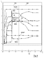
- FIG. 1 illustrates the aforementioned general principle implementing an arrangement based on two power transistors.
- This basic assembly comprises first and second power MOS transistors, type P referenced 11, 12 and connected in series, the drain D11 of the first transistor 11 being connected to the source S12 of the second transistor 12.
- a power supply 13 of 5V is connected to the source SO11 of the first transistor 11.
- An output voltage 14 connected to the drain D12 of the second transistor 12 is imposed on a potential of 0V, in the context of this Figure 1.
- the two transistors 11, 12 are 3V transistors.
- the voltage of the midpoint 15 of this arrangement (drain D11 of the first transistor 11 or source S12 of the second transistor 12) is polarized at about 2 5V. None of the transistors 11, 12 sees a voltage between two of its terminals exceeding 3.6V. Thus, none of them is stressed or runs the risk of being damaged by the potential of 5V of the power supply 13.
- the invention proposes, in a preferred embodiment, to add to the assembly of FIG. retroactive controls (not shown in Figure 1), which generate control voltages (not shown in Figure 1) applied to the gates G11, G12 transistors 11, 12 (in contrast to the case of Figure 1, the transistors are no longer mounted diode) to control them.
- these retroactive control means can be made based on a differential amplifier associated with a voltage reference.
- the differential amplifier By controlling the state (on or off) of the transistors 11 and 12, as well as the current flowing through them in the on state, the differential amplifier thus makes it possible to adjust the regulated voltage by varying the voltages across the transistors 11. , 12.
- a difficulty is that to block the first transistor 11 receiving the power supply 5V on its source S11, it is necessary that the differential amplifier provides a potential of at least 4.3V (which corresponds to 5V-VT, where VT is the threshold voltage of the diode equivalent to the first transistor 11) on the gate G11 of the first transistor 11.
- such a differential amplifier can not withstand a supply voltage greater than 3.6V and it is impossible for a differential amplifier to generate a higher voltage (> 4.3V) to the voltage with which it is powered ( ⁇ 3.6V).
- a variant of this preferred embodiment (not shown), making it possible to solve this problem (not having to block the transistor 11), would be to use the differential amplifier in order to control only the gate G12 of the second transistor 12 (which would then no longer be mounted diode), the first transistor remaining him, mounted diode.
- a first transistor 11 is used at the limit of integrability with a large channel width (for example 10000 ⁇ m) and a second transistor 12 having a channel width of 4000 ⁇ m
- the midpoint 15 is equal to 3.2V (it would be equal to 3.6V for a low current) which, when we subtract a voltage of 200mV across the second transistor 12 (of which the channel is open to the maximum because the differential amplifier imposes 0V on its gate G12), implies a regulated voltage of 3V.
- FIG. 2 illustrates a technique according to a preferred embodiment of the invention allowing, from a first intermediate control voltage REGI delivered by a differential amplifier (not shown) powered by a regulated voltage Vout less than 3.6V, to control a first transistor TP1 powered by a supply voltage VUSB of 5V.
- This technique is illustrated by means of a device 20 comprising the first power transistor TP1 and a second power transistor TP2 connected in series, such as those of FIG. 1.
- the second transistor TP2 is controlled by means of a second voltage REG.
- the device 20 can serve as a basis for the production of a regulator according to a preferred embodiment of the invention.
- means based on a differential amplifier (not shown in this FIG. 2) make it possible to generate the first intermediate control voltage REGI and the second control voltage REG.
- the first and a second transistors TP1, TP2 are P-type power MOS transistors, the drain DR1 of the first transistor TP1 being connected to the source SO2 of the second transistor TP2, which is called the middle potential 25.
- a VUSB power supply of 5V is connected to the source SO1 of the first transistor TP1.
- the drain DR2 of the second transistor TP2 is connected to a regulated voltage Vout.
- the two transistors TP1, TP2 are P-type MOS transistors 3V and are controlled at their gate GR1, GR2 respectively by the application of a first control voltage GD1 and the second control voltage REG. These voltages GD1, REG thus make it possible to control the state, either off or on, of the two transistors TP1, TP2 and each of the currents passing through them in the on state.
- the first control voltage GD1 is obtained at the output of an amplifier assembly 21 forming amplification means of the first intermediate control voltage REG1.
- the amplifier circuit 21 comprises a first and a second amplification stage 211, 212.
- the first stage 211 comprises a first amplification transistor TN1 whose gate GN1 is connected to the first control voltage REG1 and whose drain DN1 is connected. to a potential reference vssa, equal to 0V.
- Its source SN1 is connected to the drain DN2 of a second amplification transistor TN2, diode-mounted and associated in series with a third amplification transistor TN3, which is also diode-mounted.
- the drain DN3 of the third amplification transistor is connected to a potential CC, itself connected to a first amplification resistor R6 of 50 K ⁇ .
- the first resistor R6 is on the other hand connected to the VUSB power supply.
- the potential CC is also connected to the gate GP3 of a fourth amplification transistor TP3 included in the second amplification stage 212.
- the drain DP3 of the fourth amplification transistor TP3 is connected to the first control voltage GD1. even connected to a second R5 amplification resistor of 50 K ⁇ .
- the second resistor R5 is on the other hand connected to the VUSB power supply.
- the first, second and third amplification transistors TN1, TN2, TN3 are N-type MOS transistors respectively having channel widths of 4 ⁇ m, 4 ⁇ m and 6 ⁇ m.
- the fourth amplification transistor is a P-type MOS transistor having a channel width of 20 ⁇ m.
- the potential CC is approximately equal to twice the threshold voltage of one of the two diodes. equivalent to the second and third amplification transistors TN2, TN3, it is therefore approximately equal to 2V.
- the fourth amplification transistor TP3 is turned on which makes it possible to turn on the first transistor TP1.
- the potential CC is approximately equal to the supply voltage VUSB equal to approximately 5V.
- the fourth amplification transistor TP3 is blocked, which makes it possible to block the first transistor TP1.
- the amplifier assembly 21 thus makes it possible to obtain a control of the first transistor TP1 fed by a high VUSB supply voltage by means of a first lower intermediate control voltage REGI while avoiding the breakdown of this transistor by application of a too low voltage on its grid.
- FIG. 3 will show a regulating device 30 according to a preferred embodiment of the invention in which retroactive control means based on a differential amplifier are implemented.
- the regulation device 30 comprises the device 20 except that it furthermore comprises a start-up transistor TP10 forming a starting means for the device
- the latter is controlled at its gate GP10 by the regulated voltage Vout, its drain DP10 is connected to the reference potential vssa and its source SP10 is connected to the source SN2 of the second amplification transistor TN2.
- the retroactive control means comprise first and second control means.
- the first control means comprise the amplification means 21.
- the latter receiving, on the gate GN1 of the first amplification transistor TN1, the first intermediate control voltage REGI and delivering on the gate GR1 of the first transistor TP1, the first voltage GD command 1.
- the retroactive control means also comprise measuring means 31 for a measured voltage div1 which is proportional to the regulated voltage Vout.
- These measuring means 31 themselves comprise a first, a second and a third measurement resistors R1, R2, R3 of 51 K ⁇ , 500 ⁇ and 29.5 K ⁇ , respectively, which are associated in series.
- the first measurement resistor R1 is connected to the regulated voltage Vout.
- the third measurement resistor R3 is connected, in turn, to the reference potential vssa.
- the measured voltage div1 is the voltage across the second and third measurement resistors R2, R3.
- the retroactive control means further comprise means (referenced BANDGAP) for generating a reference voltage VBGP equal to 1.2V. These means are powered by the regulated voltage Vout and connected to the reference potential vssa.
- the values of the measurement resistors R1, R2, R3 are chosen so that the measured voltage div1 is equal to the reference voltage VBGP when the regulated voltage Vout is equal to the voltage that it is desired to obtain at the output of the regulator, or 3.3V, hereinafter referred to as the expected value.
- the retroactive control means furthermore comprise means for comparing the measured voltage div1 with the reference voltage VBGP.
- These comparison means themselves comprise a differential amplifier 32, powered by the regulated voltage Vout, a first input 321 receives the measured voltage div1 and a second input 322 receives the reference voltage VBGP.
- the output 323 (second input side) of the amplifier 32 delivers the first intermediate control voltage REG1 on the gate GN1 of the first amplification transistor TN1.
- the second control means 33 comprise a control resistor R4 connected, at a first end 41, to the regulated voltage Vout and at a second end 42 to the source SN4 of a control transistor TN4 whose drain DN4 is connected to the potential. reference vssa and the GN4 gate at the output 323 of the amplifier 32.
- the source SN4 of the control transistor TN4 delivers the second control voltage REG to the gate GR2 of the second transistor TP2.
- the start transistor TP10 makes it possible to turn on the first transistor TP1 when the regulating device 30 has just been powered by means of the supply voltage VUSB. Indeed, in this case, the regulated voltage Vout is equal to 0V and can not supply the differential amplifier 32 or even the voltage reference. Thus, the first control means can not control the first amplification transistor TN1 and a fortiori can not make the first transistor TP1 turn on.
- the start transistor TP10 controlled by the regulated voltage Vout, circulates a current in the first amplification resistor R6, which decreases the DC potential and thus makes it possible to turn on the fourth transistor amplification TP3 and thus to turn on the first transistor TP1.
- the fact that the first transistor TP1 is conducting causes the regulated voltage Vout to increase.
- the BANDGAP generation means begins to deliver the reference voltage VBGP at 1.2V as soon as the regulated voltage Vout reaches 1.4V.
- the differential amplifier 32 only starts to operate as soon as the regulated voltage Vout reaches 1.8V.
- the retroactive control means take control of the first and second transistors TP1, TP2 so as to continue to increase the regulated voltage Vout until it reaches the expected value of 3.3V, from which they block the first and second transistors TP1, TP2 in order to stabilize the regulated voltage.
- the starting transistor TP10 becomes off.
- the measured voltage div1 which is proportional to the latter, becomes lower than the value of the reference voltage VBGP of 1.2V, and thus the first intermediate control voltage REG1 (output of the differential amplifier 32 of the comparator arrangement) increases.
- This has the effect of opening the first amplification transistor TN1 as soon as the latter reaches 1.8V, which causes the opening of the fourth amplification transistor TP3, itself causing the opening of the first transistor TP1.
- This also has the effect of decreasing the second control voltage REG which thus opens the second transistor TP2.
- the openings of the first and second transistors TP1, TP2 result in an increase of the regulated voltage until it reaches its expected value of 3.3V.
- Closing the first transistor TP1 results in a decrease in the regulated voltage until it reaches its expected value of 3.3V.
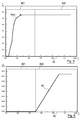
- the regulated voltage Vout is constant and equal to 3.3 V despite the current draw made by the load placed at the output of the regulator from 0.5 ms.
- FIG. 6 representing the linear evolution of this current as a function of time 43.
- the amplification means may be made in any other way, in particular from an operational amplifier.
- the transistors of the embodiments mentioned above can be replaced by any type of transistor and in particular field effect transistors.
- the type of transistors mentioned can be inverted, it is thus possible to use P type transistors instead of N type transistors and vice versa depending on the intended applications.
Landscapes
- Engineering & Computer Science (AREA)
- Physics & Mathematics (AREA)
- Electromagnetism (AREA)
- General Physics & Mathematics (AREA)
- Radar, Positioning & Navigation (AREA)
- Automation & Control Theory (AREA)
- Continuous-Control Power Sources That Use Transistors (AREA)
Applications Claiming Priority (1)
| Application Number | Priority Date | Filing Date | Title |
|---|---|---|---|
| FR0413445A FR2879771B1 (fr) | 2004-12-16 | 2004-12-16 | Dispositif de regulation haute tension compatible avec les technologies basses tensions et circuit electronique correspondant |
Publications (2)
| Publication Number | Publication Date |
|---|---|
| EP1724656A2 true EP1724656A2 (de) | 2006-11-22 |
| EP1724656A3 EP1724656A3 (de) | 2007-03-07 |
Family
ID=34953140
Family Applications (1)
| Application Number | Title | Priority Date | Filing Date |
|---|---|---|---|
| EP05111836A Withdrawn EP1724656A3 (de) | 2004-12-16 | 2005-12-08 | Vorrichtung zur Hochspannungsregelung kompatibel mit Niederspannungstechnologie und entsprechende elektronische Schaltung |
Country Status (3)
| Country | Link |
|---|---|
| US (1) | US7525294B2 (de) |
| EP (1) | EP1724656A3 (de) |
| FR (1) | FR2879771B1 (de) |
Families Citing this family (7)
| Publication number | Priority date | Publication date | Assignee | Title |
|---|---|---|---|---|
| US7755419B2 (en) | 2006-01-17 | 2010-07-13 | Cypress Semiconductor Corporation | Low power beta multiplier start-up circuit and method |
| US7830200B2 (en) * | 2006-01-17 | 2010-11-09 | Cypress Semiconductor Corporation | High voltage tolerant bias circuit with low voltage transistors |
| CN101408564A (zh) * | 2008-11-18 | 2009-04-15 | 上海贝岭矽创微电子有限公司 | 电压检测电路 |
| KR20110123544A (ko) * | 2010-05-07 | 2011-11-15 | 삼성전자주식회사 | 반도체 장치 및 그 제조 방법 |
| US8957647B2 (en) * | 2010-11-19 | 2015-02-17 | Taiwan Semiconductor Manufacturing Co., Ltd. | System and method for voltage regulation using feedback to active circuit element |
| FR3032309B1 (fr) * | 2015-02-02 | 2017-06-23 | St Microelectronics Alps Sas | Circuit de regulation de tension adapte aux fortes et faibles puissances |
| US12045074B1 (en) * | 2022-12-29 | 2024-07-23 | Texas Instruments Incorporated | Bandgap voltage reference circuit topology including a feedback circuit with a scaling amplifier |
Family Cites Families (7)
| Publication number | Priority date | Publication date | Assignee | Title |
|---|---|---|---|---|
| US4278929A (en) * | 1979-11-21 | 1981-07-14 | Motorola, Inc. | Regulated negative voltage supply |
| EP1061428B1 (de) * | 1999-06-16 | 2005-08-31 | STMicroelectronics S.r.l. | BICMOS / CMOS Spannungsregler mit kleiner Verlustspannung |
| JP2002008374A (ja) * | 2000-06-22 | 2002-01-11 | Mitsubishi Electric Corp | 電圧降圧回路 |
| WO2004092861A1 (en) * | 2003-04-16 | 2004-10-28 | Koninklijke Philips Electronics N.V. | Voltage regulation system comprising operating condition detection means |
| JP3670653B2 (ja) * | 2003-04-21 | 2005-07-13 | 株式会社東芝 | Dc−dcコンバータ制御回路、及び、dc−dcコンバータ |
| EP1892600B1 (de) * | 2006-08-24 | 2016-07-27 | Micron Technology, Inc. | Spannungsregler für nichtflüchtige speichereinheiten mit niedrigspannungstransistoren |
| EP1916586B1 (de) * | 2006-10-23 | 2018-09-05 | Dialog Semiconductor GmbH | Regulierter Analogschalter |
-
2004
- 2004-12-16 FR FR0413445A patent/FR2879771B1/fr not_active Expired - Fee Related
-
2005
- 2005-12-08 EP EP05111836A patent/EP1724656A3/de not_active Withdrawn
- 2005-12-15 US US11/303,739 patent/US7525294B2/en active Active
Also Published As
| Publication number | Publication date |
|---|---|
| EP1724656A3 (de) | 2007-03-07 |
| FR2879771B1 (fr) | 2007-06-22 |
| US20060170407A1 (en) | 2006-08-03 |
| FR2879771A1 (fr) | 2006-06-23 |
| US7525294B2 (en) | 2009-04-28 |
Similar Documents
| Publication | Publication Date | Title |
|---|---|---|
| EP3249491B1 (de) | Vorrichtung zum regulieren eines schwachen spannungsabfalls, die insbesondere in der lage ist, versorgungsspannungen zu unterstützen, die mit der usb-norm typ c kompatibel sind | |
| EP0289370B1 (de) | Spannungshochniveaudetektionsanordnung in der MOS-technologie | |
| FR2755318A1 (fr) | Circuit regulateur et dispositif a circuit integre a semi-conducteur le comprenant | |
| FR2554990A1 (fr) | Circuit regulateur de tension serie | |
| FR3102581A1 (fr) | Régulateur de tension | |
| FR2677793A1 (fr) | Circuit pour produire une tension d'alimentation interne. | |
| EP0583203B1 (de) | Schaltung zum Ziehen des Eingangs einer integrierten Schaltung auf einen definierten Zustand | |
| FR3102580A1 (fr) | Régulateur de tension | |
| EP0678802B1 (de) | Schaltungsanordnung zur Spannungsbegrenzung mit Hysteresiskomparator | |
| FR2770004A1 (fr) | Generateur de courant constant precis | |
| EP1724656A2 (de) | Vorrichtung zur Hochspannungsregelung kompatibel mit Niederspannungstechnologie und entsprechende elektronische Schaltung | |
| EP1380913A1 (de) | Linearer Spannungsregler | |
| EP0756223A1 (de) | Spannungs- und/oder Stromreferenzgenerator in integriertem Schaltkreis | |
| FR3072841A1 (fr) | Circuit electronique avec dispositif de surveillance de l'alimentation utilisant un seuil de declenchement choisi dans une plage de tensions autour d'une tension de bande interdite | |
| FR3053857A1 (fr) | Circuit de selection d'une tension d'alimentation a transition controlee | |
| FR2957732A1 (fr) | Etage de sortie d'un circuit electronique | |
| EP0829796A1 (de) | Spannungssteuerung mit gedämpfter Temperaturempfindlichkeit | |
| FR2802315A1 (fr) | Regulateur de tension a transistor ballast et a limiteur de courant | |
| FR3072842A1 (fr) | Circuit electronique avec dispositif de surveillance de l'alimentation | |
| EP1258975B1 (de) | Regelungsschaltung für Hochspannungsgenerator | |
| EP0538121A1 (de) | Anordnung zum Generieren einer programmierspannung eines programmierbaren Festwertspeichers, insbesondere des EPROM-Typs, und dazugehörige Verfahren und Speicher | |
| EP2648332B1 (de) | Vorrichtung zum Polarisieren von Vorverstärkern | |
| FR2925184A1 (fr) | Regulateur de tension a boucle auto-adaptative | |
| FR2783617A1 (fr) | Systeme de regulation d'une pompe de charge | |
| EP0050583A1 (de) | Wechselspannung/Gleichstrom-Konverter und Schwingkreis-Schaltung mit einem solchen Konverter |
Legal Events
| Date | Code | Title | Description |
|---|---|---|---|
| PUAI | Public reference made under article 153(3) epc to a published international application that has entered the european phase |
Free format text: ORIGINAL CODE: 0009012 |
|
| AK | Designated contracting states |
Kind code of ref document: A2 Designated state(s): AT BE BG CH CY CZ DE DK EE ES FI FR GB GR HU IE IS IT LI LT LU LV MC NL PL PT RO SE SI SK TR |
|
| AX | Request for extension of the european patent |
Extension state: AL BA HR MK YU |
|
| PUAL | Search report despatched |
Free format text: ORIGINAL CODE: 0009013 |
|
| AK | Designated contracting states |
Kind code of ref document: A3 Designated state(s): AT BE BG CH CY CZ DE DK EE ES FI FR GB GR HU IE IS IT LI LT LU LV MC NL PL PT RO SE SI SK TR |
|
| AX | Request for extension of the european patent |
Extension state: AL BA HR MK YU |
|
| 17P | Request for examination filed |
Effective date: 20070426 |
|
| AKX | Designation fees paid |
Designated state(s): DE ES GB IT NL |
|
| 17Q | First examination report despatched |
Effective date: 20080125 |
|
| STAA | Information on the status of an ep patent application or granted ep patent |
Free format text: STATUS: THE APPLICATION IS DEEMED TO BE WITHDRAWN |
|
| 18D | Application deemed to be withdrawn |
Effective date: 20110701 |