EP1724885A1 - Circuit de commande pour élément électronique - Google Patents
Circuit de commande pour élément électronique Download PDFInfo
- Publication number
- EP1724885A1 EP1724885A1 EP06017001A EP06017001A EP1724885A1 EP 1724885 A1 EP1724885 A1 EP 1724885A1 EP 06017001 A EP06017001 A EP 06017001A EP 06017001 A EP06017001 A EP 06017001A EP 1724885 A1 EP1724885 A1 EP 1724885A1
- Authority
- EP
- European Patent Office
- Prior art keywords
- circuit
- driver circuit
- transistor
- current
- supply voltage
- Prior art date
- Legal status (The legal status is an assumption and is not a legal conclusion. Google has not performed a legal analysis and makes no representation as to the accuracy of the status listed.)
- Withdrawn
Links
- 239000003990 capacitor Substances 0.000 claims description 5
- 230000005669 field effect Effects 0.000 claims description 4
- 238000013016 damping Methods 0.000 claims description 2
- 230000001052 transient effect Effects 0.000 abstract description 16
- 238000000034 method Methods 0.000 abstract description 6
- 230000008569 process Effects 0.000 abstract description 5
- 238000006073 displacement reaction Methods 0.000 description 10
- 230000009467 reduction Effects 0.000 description 10
- 230000001419 dependent effect Effects 0.000 description 8
- 230000008901 benefit Effects 0.000 description 6
- 238000010586 diagram Methods 0.000 description 6
- 239000000758 substrate Substances 0.000 description 5
- 230000004044 response Effects 0.000 description 4
- 230000008859 change Effects 0.000 description 3
- 238000005516 engineering process Methods 0.000 description 3
- 230000003071 parasitic effect Effects 0.000 description 2
- 230000002123 temporal effect Effects 0.000 description 2
- 230000003321 amplification Effects 0.000 description 1
- 230000005540 biological transmission Effects 0.000 description 1
- 239000002800 charge carrier Substances 0.000 description 1
- 239000004020 conductor Substances 0.000 description 1
- 238000010276 construction Methods 0.000 description 1
- 230000003503 early effect Effects 0.000 description 1
- 230000000694 effects Effects 0.000 description 1
- 230000002349 favourable effect Effects 0.000 description 1
- 238000002955 isolation Methods 0.000 description 1
- 238000004519 manufacturing process Methods 0.000 description 1
- 238000003199 nucleic acid amplification method Methods 0.000 description 1
- 230000003287 optical effect Effects 0.000 description 1
- 238000004806 packaging method and process Methods 0.000 description 1
- 239000004065 semiconductor Substances 0.000 description 1
- 239000007787 solid Substances 0.000 description 1
- 238000003860 storage Methods 0.000 description 1
- 239000013589 supplement Substances 0.000 description 1
- 230000007704 transition Effects 0.000 description 1
- 230000001960 triggered effect Effects 0.000 description 1
- 238000009827 uniform distribution Methods 0.000 description 1
Images


Classifications
-
- H—ELECTRICITY
- H01—ELECTRIC ELEMENTS
- H01S—DEVICES USING THE PROCESS OF LIGHT AMPLIFICATION BY STIMULATED EMISSION OF RADIATION [LASER] TO AMPLIFY OR GENERATE LIGHT; DEVICES USING STIMULATED EMISSION OF ELECTROMAGNETIC RADIATION IN WAVE RANGES OTHER THAN OPTICAL
- H01S5/00—Semiconductor lasers
- H01S5/04—Processes or apparatus for excitation, e.g. pumping, e.g. by electron beams
- H01S5/042—Electrical excitation ; Circuits therefor
-
- G—PHYSICS
- G05—CONTROLLING; REGULATING
- G05F—SYSTEMS FOR REGULATING ELECTRIC OR MAGNETIC VARIABLES
- G05F3/00—Non-retroactive systems for regulating electric variables by using an uncontrolled element, or an uncontrolled combination of elements, such element or such combination having self-regulating properties
- G05F3/02—Regulating voltage or current
- G05F3/08—Regulating voltage or current wherein the variable is DC
- G05F3/10—Regulating voltage or current wherein the variable is DC using uncontrolled devices with non-linear characteristics
- G05F3/16—Regulating voltage or current wherein the variable is DC using uncontrolled devices with non-linear characteristics being semiconductor devices
- G05F3/20—Regulating voltage or current wherein the variable is DC using uncontrolled devices with non-linear characteristics being semiconductor devices using diode- transistor combinations
- G05F3/26—Current mirrors
- G05F3/265—Current mirrors using bipolar transistors only
-
- H—ELECTRICITY
- H01—ELECTRIC ELEMENTS
- H01S—DEVICES USING THE PROCESS OF LIGHT AMPLIFICATION BY STIMULATED EMISSION OF RADIATION [LASER] TO AMPLIFY OR GENERATE LIGHT; DEVICES USING STIMULATED EMISSION OF ELECTROMAGNETIC RADIATION IN WAVE RANGES OTHER THAN OPTICAL
- H01S5/00—Semiconductor lasers
- H01S5/04—Processes or apparatus for excitation, e.g. pumping, e.g. by electron beams
- H01S5/042—Electrical excitation ; Circuits therefor
- H01S5/0428—Electrical excitation ; Circuits therefor for applying pulses to the laser
Definitions
- the invention relates to a driver circuit for operating an electronic component with an electrically variable current, which is reversed in a controlled manner between at least two discrete currents, according to the preamble of patent claim 1.
- Laser diodes are an example of an electronic device that operates with such a driver circuit.
- a driver circuit for operating laser diodes which has circuit elements that attenuate transients that occur when the electrically variable current is reversed between the at least two discrete currents.
- Laser diode-based semiconductor lasers are used, for example, for writing data in storage media such as CD and DVD.
- High speed writing requires optical pulses of light with precise timing and precision.
- drive circuits are therefore required which can deliver current pulses of defined height and with precise temporal behavior.
- a driver circuit which comprises a current mirror circuit having a first series circuit of a reference resistor and a reference transistor between a supply voltage terminal and a control current source and a second series circuit of a further resistor and another transistor between the supply voltage terminal and an output of the current mirror circuit, wherein both the reference transistor as well as the further transistor are controlled by a common control power source.
- the displacement current is only amplified by the effective collector-base capacitance of the driver circuit with a mirror factor K (f) dropping above the frequency.
- the displacement current flows essentially via the reference transistor and the resistor in the reference branch to the supply voltage.
- the capacity is realized by a plurality of individual capacities.
- the inductance is realized by interposing a conductive connection between the first supply voltage terminal and the second supply voltage terminal.
- an n-well of a pnp transistor or a p-well of an npn transistor is connected via a damping resistor to a reference potential.
- the numeral 48 denotes a second series circuit of a further resistor 50 and a further transistor 52.
- the second series circuit 48 is located between the supply voltage input 18 and the control signal output 30 of the driver circuit 16.
- the control current source 46 controls both the reference transistor 44 and the further transistor 52nd
- the current I_LD required for driving the laser diode 36 is provided by the further transistor 52 which implements a current mirror circuit 38 in conjunction with the reference transistor 44.
- the task of the current mirror circuit 38 is to amplify the control current 10 by a factor K that is as precisely defined as possible. To achieve this, the following conditions must be met.
- the resistors 42 and 50 bring about a uniform distribution of current in the transistors 44 and 52 realized by a plurality of emitter fingers.
- the further resistor 50 also causes a reduction of the so-called early effects, which leads to an undesired dependence of the output current I_LD on the collector-emitter. Voltage of the transistors 44 and 52 leads.
- the disturbing inductances are located both in the Driver module 14 in the form of bonding wire inductances and Gesimousinduktriosen, as well as outside in the supply lines for the supply voltage and for the supply of the laser diode 36. These inductors can not be completely avoided with today's construction technique. Values for the bond wire inductances are in the range of about 1 nH.
- unavoidable capacitances 74, 76 of the illustrated pnp transistor are formed in the layers in which the charge carrier concentration transitions from a first concentration to a second concentration.
- the numeral 74 denotes such an unavoidable collector-base capacity.
- numeral 76 designates the unavoidable capacitance between collector layer 66 and n-well 70
- numeral 78 designates the unavoidable capacitance between n-well 70 and p-substrate 72. Both parasitic inductances are desirable for favorable transient response as well as to minimize the parasitic capacities as much as possible.
- the capacitances shown in FIG. 5 need not be reduced further. However, their influence on the transient response can be influenced by suitable circuit measures. This is especially true for the capacitance 74 of the collector-base junction.
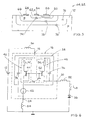
- FIG. 6 shows the circuit arrangement according to FIG. 2 with supplements by line inductances and transistor capacitances, as occur in a real circuit.
- this includes the inductance 80 of the supply line between the supply voltage source 12 and supply voltage input 18, an inductance 82 of the control line between the control signal output 30 of the driver circuit 16 and the laser diode 36 to be controlled, and the inductance 84 of the ground terminal 24 of the driver circuit 16.
- the collector-base capacitance 74 affects in particular the further transistor 52, so the driver transistor from. It is therefore shown in FIG. 6 between the control input (base) of the further transistor 52 and its collector.
- the collector-well capacitance 76 is in the circuit diagram of Figure 6 parallel to the second series circuit 48 of further resistor 50 and further transistor 52.
- the well-substrate capacitance 78 is in the diagram of Figure 6 between the supply voltage input 18 and the ground terminal 24th
- circuit measures are presented below which influence the transient response in a desired manner by generating a frequency-dependent amplification factor K of the current mirror circuit 38.
- the effective collector-base capacitance 74 can be substantially reduced.
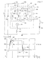
- this is achieved by inserting the inductance 86 into the connection of the supply line inductance 80 with the second series circuit 48 of further resistor 50 and further transistor (driver transistor) 52.
- the inductance 86 can be switched outside the driver circuit 16, so that the inductance 86 is connected to a second supply voltage input 87 of the driver circuit 16.
- the inductance 86 can thus be realized, for example, as a bonding wire.
- a capacitor 88 can be connected in parallel to the reference resistor 42.
- the displacement current of the collector-base capacitance 74 is amplified only with the falling over the frequency mirror factor K (f). In other words, it is exploited that the effect of the collector-base capacitance 74 scales with the mirror ratio K (f).
- FIG. 7 also shows that the collector-well capacitance 76, that is to say the n-well 70 required for insulating the transistors, has been connected to the supply voltage input 18 via a resistor 90.
- the collector-well-capacity 76th flowing displacement current can flow directly to the supply voltage.
- the n-well 70 is kept at a constant potential.
- Undesirable displacement currents that might otherwise occur as a result of the relatively large capacitance 78 between well 70 and substrate 72 are kept so small.
- the resistor 90 has the function of reducing the quality of the resonant circuit produced in conjunction with the inductance 82 of the drive line, which keeps the amplitude of the transient processes low.
- the backup capacitor 100 shown in FIG. 7 reduces the influence of the bond wire inductances 80 in the supply of the supply voltage for the driver chip to the driver circuit 16.
- FIG. 8 shows time profiles of the drive current I_LD for the laser diode 36, as calculated for various values of the inductance 86.
- the curve 92 corresponds to a non-existent inductance 86.
- the curve 94 was calculated with a value of 300 pH for the inductance 86 at an inductance 82 of the drive line of 3 nH. As can be seen in Figure 8, turning on such an inductor 86 at 300 pH reduces the amplitude of the transients. Further reduction is achieved by switching on an inductance of 86 from 600 pH. The result for this value is represented by the curve 96. As can be seen from the course of the curve 96, the Transient processes with almost constant slope are almost completely avoided.
- Comparable results are obtained when switching on a capacitor 88 in the manner shown in FIG. Furthermore, comparable results are obtained with a combination of a capacitance 88 with an inductance 86.
- the dimensioning of the circuit and thus the dimensioning of the capacitance 88 and / or the inductance 86 depends on the technical boundary conditions such as the bonding wire length, the inductance of the load (the laser diode 36) as well as the requirements for the rise times and decay times of the drive signal.
Landscapes
- Engineering & Computer Science (AREA)
- Physics & Mathematics (AREA)
- Microelectronics & Electronic Packaging (AREA)
- General Physics & Mathematics (AREA)
- Electromagnetism (AREA)
- Radar, Positioning & Navigation (AREA)
- Nonlinear Science (AREA)
- Automation & Control Theory (AREA)
- Condensed Matter Physics & Semiconductors (AREA)
- Optics & Photonics (AREA)
- Semiconductor Lasers (AREA)
- Control Of Electrical Variables (AREA)
- Electronic Switches (AREA)
Applications Claiming Priority (2)
| Application Number | Priority Date | Filing Date | Title |
|---|---|---|---|
| DE10323669A DE10323669A1 (de) | 2003-05-14 | 2003-05-14 | Treiberschaltung zum Betreiben eines elektronischen Bauteils |
| EP04011125A EP1478063B1 (fr) | 2003-05-14 | 2004-05-11 | Circuit de commande pour élement electronique |
Related Parent Applications (1)
| Application Number | Title | Priority Date | Filing Date |
|---|---|---|---|
| EP04011125A Division EP1478063B1 (fr) | 2003-05-14 | 2004-05-11 | Circuit de commande pour élement electronique |
Publications (1)
| Publication Number | Publication Date |
|---|---|
| EP1724885A1 true EP1724885A1 (fr) | 2006-11-22 |
Family
ID=33016453
Family Applications (2)
| Application Number | Title | Priority Date | Filing Date |
|---|---|---|---|
| EP04011125A Expired - Lifetime EP1478063B1 (fr) | 2003-05-14 | 2004-05-11 | Circuit de commande pour élement electronique |
| EP06017001A Withdrawn EP1724885A1 (fr) | 2003-05-14 | 2004-05-11 | Circuit de commande pour élément électronique |
Family Applications Before (1)
| Application Number | Title | Priority Date | Filing Date |
|---|---|---|---|
| EP04011125A Expired - Lifetime EP1478063B1 (fr) | 2003-05-14 | 2004-05-11 | Circuit de commande pour élement electronique |
Country Status (6)
| Country | Link |
|---|---|
| US (1) | US7145929B2 (fr) |
| EP (2) | EP1478063B1 (fr) |
| JP (1) | JP2004342089A (fr) |
| KR (1) | KR100740359B1 (fr) |
| CN (1) | CN1551702A (fr) |
| DE (2) | DE10323669A1 (fr) |
Families Citing this family (28)
| Publication number | Priority date | Publication date | Assignee | Title |
|---|---|---|---|---|
| US6931040B2 (en) * | 2003-06-20 | 2005-08-16 | Maxim Integrated Products, Inc. | System and method for using an output transformer for laser diode drivers |
| CN100454695C (zh) * | 2006-03-20 | 2009-01-21 | 中兴通讯股份有限公司 | 同轴直调激光器耦合驱动电路 |
| JP2007305762A (ja) * | 2006-05-11 | 2007-11-22 | Mitsubishi Electric Corp | レーザダイオードの駆動回路 |
| US7646988B2 (en) * | 2006-08-04 | 2010-01-12 | Finisar Corporation | Linear amplifier for use with laser driver signal |
| US7734184B2 (en) * | 2006-08-04 | 2010-06-08 | Finisar Corporation | Optical transceiver module having an active linear optoelectronic device |
| CN201025532Y (zh) * | 2007-02-27 | 2008-02-20 | 鸿富锦精密工业(深圳)有限公司 | 电脑测试装置 |
| DE102008014425B4 (de) | 2008-03-13 | 2012-03-29 | Atmel Automotive Gmbh | Treiberschaltung mit einem Dämpfungsnetzwerk unter Verwendung eines Stromspiegels |
| DE602009000366D1 (de) * | 2008-04-25 | 2010-12-30 | Jds Uniphase Corp | Gleichstromgekoppelter Antrieb mit aktiver Terminierung |
| JP5343510B2 (ja) * | 2008-10-29 | 2013-11-13 | ミツミ電機株式会社 | 半導体装置 |
| WO2012085800A1 (fr) * | 2010-12-21 | 2012-06-28 | Koninklijke Philips Electronics N.V. | Dispositif et procédé de commande du courant d'un circuit d'éclairage à semiconducteurs |
| US9706610B2 (en) | 2011-10-18 | 2017-07-11 | Atmel Corporation | Driving circuits for light emitting elements |
| CN104124957B (zh) * | 2014-08-14 | 2017-02-15 | 灿芯半导体(上海)有限公司 | 电平转换电路 |
| WO2016083251A1 (fr) * | 2014-11-24 | 2016-06-02 | Bang & Olufsen A/S | Relais de commutation à semi-conducteurs |
| US11466316B2 (en) | 2015-05-20 | 2022-10-11 | Quantum-Si Incorporated | Pulsed laser and bioanalytic system |
| US10605730B2 (en) | 2015-05-20 | 2020-03-31 | Quantum-Si Incorporated | Optical sources for fluorescent lifetime analysis |
| BR112017024605B1 (pt) * | 2015-05-20 | 2022-11-16 | Quantum-Si Incorporated | Fonte óptica pulsada e método com a finalidade de produzir um pulso óptico com uma fonte óptica pulsada |
| CA3040184C (fr) * | 2016-10-14 | 2022-06-07 | Waymo Llc | Ganfet en tant que stockage d'energie destine a un generateur d'impulsions laser rapide |
| CA3047133A1 (fr) | 2016-12-16 | 2018-06-21 | Quantum-Si Incorporated | Module laser compact a verrouillage de mode |
| CN116466494A (zh) | 2016-12-16 | 2023-07-21 | 宽腾矽公司 | 紧密的光束整形及操纵总成 |
| US10317925B2 (en) * | 2017-03-29 | 2019-06-11 | Texas Instruments Incorporated | Attenuating common mode noise current in current mirror circuits |
| CA3100987A1 (fr) | 2018-06-15 | 2019-12-19 | Quantum-Si Incorporated | Commande d'acquisition de donnees pour instruments analytiques perfectionnes ayant des sources optiques pulsees |
| CN108983860B (zh) * | 2018-09-18 | 2024-01-12 | 杭州洪芯微电子科技有限公司 | 基于电压校准的电流自检调节电路 |
| CN111384662B (zh) * | 2018-12-28 | 2021-09-17 | 深圳市傲科光电子有限公司 | 直调激光器驱动电路以及直调激光器系统 |
| EP4411347A3 (fr) | 2019-06-14 | 2024-10-30 | Quantum-Si Incorporated | Coupleur à réseau tranché à sensibilité d'alignement de faisceau accrue |
| CN115210969A (zh) | 2020-01-14 | 2022-10-18 | 宽腾矽公司 | 调幅激光器 |
| US11482836B2 (en) * | 2020-01-28 | 2022-10-25 | Stmicroelectronics (Grenoble 2) Sas | Laser diode driver circuits and methods of operating thereof |
| US11442485B2 (en) * | 2020-07-09 | 2022-09-13 | Novatek Microelectronics Corp. | Integrated circuit chip and test method thereof |
| GB202013640D0 (en) * | 2020-08-31 | 2020-10-14 | Ams Sensor Asia Pte Ltd | Self-calibrating driver circuit |
Citations (12)
| Publication number | Priority date | Publication date | Assignee | Title |
|---|---|---|---|---|
| US4567444A (en) * | 1983-05-26 | 1986-01-28 | Sony Corporation | Current mirror circuit with control means for establishing an input-output current ratio |
| EP0257345A2 (fr) * | 1986-08-21 | 1988-03-02 | Tektronix Inc. | Miroir de courant compensé |
| JPH04239188A (ja) * | 1991-01-11 | 1992-08-27 | Nec Corp | レーザダイオード駆動回路 |
| JPH04275473A (ja) * | 1991-03-02 | 1992-10-01 | Sumitomo Electric Ind Ltd | レーザダイオード駆動回路 |
| US5177451A (en) * | 1991-07-26 | 1993-01-05 | Burr-Brown Corporation | Unity gain amplifier with high slew rate and high bandwidth |
| JPH05259546A (ja) * | 1992-03-10 | 1993-10-08 | Nec Corp | レーザダイオード駆動回路 |
| EP0707255A1 (fr) * | 1994-10-13 | 1996-04-17 | AT&T Corp. | Circuit d'attaque pour diodes électroluminescentes composé de miroirs de courant multipliants en cascade |
| EP0756362A1 (fr) * | 1995-07-28 | 1997-01-29 | Nec Corporation | Circuit de commande de diode laser commandé en tension |
| EP0810700A2 (fr) * | 1996-05-03 | 1997-12-03 | Xerox Corporation | Système d'atténuation des oscillations de hautes fréquences sur-puce pour des circuits de commande |
| US5796767A (en) * | 1996-02-20 | 1998-08-18 | Nec Corporation | Driver circuit of light-emitting device |
| JP2001036187A (ja) * | 1999-07-22 | 2001-02-09 | Sony Corp | レーザーダイオードの駆動回路及び光情報処理装置 |
| WO2003034558A1 (fr) * | 2001-10-11 | 2003-04-24 | Hamamatsu Photonics K.K. | Circuit d'attaque d'un element electroluminescent |
Family Cites Families (6)
| Publication number | Priority date | Publication date | Assignee | Title |
|---|---|---|---|---|
| JPH0795610B2 (ja) * | 1991-01-17 | 1995-10-11 | インターナショナル・ビジネス・マシーンズ・コーポレイション | レーザ駆動装置及び光ディスク駆動装置 |
| US6272160B1 (en) * | 1998-02-03 | 2001-08-07 | Applied Micro Circuits Corporation | High-speed CMOS driver for vertical-cavity surface-emitting lasers |
| US6516015B1 (en) * | 1998-11-19 | 2003-02-04 | Matsushita Electric Industrial Co., Ltd. | Laser driver and optical transceiver |
| US6794880B2 (en) * | 2002-02-14 | 2004-09-21 | Renesas Technology America, Inc. | Methods and apparatus for detecting terminal open circuits and short circuits to ground in inductive head write driver circuits |
| TW550977B (en) * | 2002-02-15 | 2003-09-01 | Ind Tech Res Inst | Control circuit for driving light emitting device |
| JP2005026410A (ja) * | 2003-07-01 | 2005-01-27 | Ricoh Co Ltd | 半導体レーザ駆動装置 |
-
2003
- 2003-05-14 DE DE10323669A patent/DE10323669A1/de not_active Withdrawn
-
2004
- 2004-03-30 JP JP2004099844A patent/JP2004342089A/ja not_active Withdrawn
- 2004-05-11 DE DE502004002598T patent/DE502004002598D1/de not_active Expired - Lifetime
- 2004-05-11 EP EP04011125A patent/EP1478063B1/fr not_active Expired - Lifetime
- 2004-05-11 EP EP06017001A patent/EP1724885A1/fr not_active Withdrawn
- 2004-05-13 US US10/846,836 patent/US7145929B2/en not_active Expired - Fee Related
- 2004-05-13 KR KR1020040033911A patent/KR100740359B1/ko not_active Expired - Fee Related
- 2004-05-14 CN CNA2004100431992A patent/CN1551702A/zh active Pending
Patent Citations (12)
| Publication number | Priority date | Publication date | Assignee | Title |
|---|---|---|---|---|
| US4567444A (en) * | 1983-05-26 | 1986-01-28 | Sony Corporation | Current mirror circuit with control means for establishing an input-output current ratio |
| EP0257345A2 (fr) * | 1986-08-21 | 1988-03-02 | Tektronix Inc. | Miroir de courant compensé |
| JPH04239188A (ja) * | 1991-01-11 | 1992-08-27 | Nec Corp | レーザダイオード駆動回路 |
| JPH04275473A (ja) * | 1991-03-02 | 1992-10-01 | Sumitomo Electric Ind Ltd | レーザダイオード駆動回路 |
| US5177451A (en) * | 1991-07-26 | 1993-01-05 | Burr-Brown Corporation | Unity gain amplifier with high slew rate and high bandwidth |
| JPH05259546A (ja) * | 1992-03-10 | 1993-10-08 | Nec Corp | レーザダイオード駆動回路 |
| EP0707255A1 (fr) * | 1994-10-13 | 1996-04-17 | AT&T Corp. | Circuit d'attaque pour diodes électroluminescentes composé de miroirs de courant multipliants en cascade |
| EP0756362A1 (fr) * | 1995-07-28 | 1997-01-29 | Nec Corporation | Circuit de commande de diode laser commandé en tension |
| US5796767A (en) * | 1996-02-20 | 1998-08-18 | Nec Corporation | Driver circuit of light-emitting device |
| EP0810700A2 (fr) * | 1996-05-03 | 1997-12-03 | Xerox Corporation | Système d'atténuation des oscillations de hautes fréquences sur-puce pour des circuits de commande |
| JP2001036187A (ja) * | 1999-07-22 | 2001-02-09 | Sony Corp | レーザーダイオードの駆動回路及び光情報処理装置 |
| WO2003034558A1 (fr) * | 2001-10-11 | 2003-04-24 | Hamamatsu Photonics K.K. | Circuit d'attaque d'un element electroluminescent |
Non-Patent Citations (4)
| Title |
|---|
| PATENT ABSTRACTS OF JAPAN vol. 017, no. 006 (E - 1302) 7 January 1993 (1993-01-07) * |
| PATENT ABSTRACTS OF JAPAN vol. 017, no. 071 (E - 1319) 12 February 1993 (1993-02-12) * |
| PATENT ABSTRACTS OF JAPAN vol. 018, no. 022 (E - 1490) 13 January 1994 (1994-01-13) * |
| PATENT ABSTRACTS OF JAPAN vol. 2000, no. 19 5 June 2001 (2001-06-05) * |
Also Published As
| Publication number | Publication date |
|---|---|
| US7145929B2 (en) | 2006-12-05 |
| DE10323669A1 (de) | 2004-12-02 |
| US20040257140A1 (en) | 2004-12-23 |
| CN1551702A (zh) | 2004-12-01 |
| EP1478063A3 (fr) | 2005-11-16 |
| JP2004342089A (ja) | 2004-12-02 |
| EP1478063A2 (fr) | 2004-11-17 |
| EP1478063B1 (fr) | 2007-01-10 |
| DE502004002598D1 (de) | 2007-02-22 |
| KR100740359B1 (ko) | 2007-07-16 |
| KR20040098579A (ko) | 2004-11-20 |
Similar Documents
| Publication | Publication Date | Title |
|---|---|---|
| EP1478063B1 (fr) | Circuit de commande pour élement electronique | |
| DE3523400C2 (de) | Schaltungsanordnung für eine Ausgangsstufe der Klasse AB mit großer Schwingungsweite | |
| DE3904901C2 (fr) | ||
| WO2019057236A1 (fr) | Circuit de commande de laser intégré pour la commande d'un courant pulsé pour une diode laser | |
| EP0562359B1 (fr) | Circuit pour commander une diode laser | |
| EP2101241A1 (fr) | Circuit de commande, methode et utilisation d'un miroir de courant d'un circuit de commande | |
| EP0000169B1 (fr) | Condensateur à jonction semiconducteur dans un mode intégré de construction et circuit du type bootstrap avec un tel condensateur | |
| DE19620839C2 (de) | Operationsverstärker | |
| DE19633971C2 (de) | Stromversorgung zum Betrieb einer integrierten Schaltung | |
| DE102021111003B4 (de) | Dual-mode-versorgungsschaltung und verfahren | |
| DE3615383C2 (de) | Eine Schaltung zur Verschiebung des Eingangspegels eines Digital-Analog-Wandlers | |
| DE2853581C2 (de) | Emitterfolgerschaltung | |
| EP0604485B1 (fr) | Dispositif de generation de tensions intermediaires | |
| EP1317793B1 (fr) | Circuit a pompe de charge | |
| DE69126734T2 (de) | Verzögerungsglied mit steuerbarer Verzögerung | |
| DE3546204C2 (de) | Monolithisch integrierte Signalverstärkersstufe mit hoher Ausgangsdynamik | |
| DE3739872C2 (fr) | ||
| EP0277377A1 (fr) | Circuit à limitation de courant | |
| DE3615382C2 (de) | Digital-Analog-Wandler mit einer Bit-Einstell- und Filterschaltung | |
| DE3615513A1 (de) | Digital-analog-wandler fuer niedrige spannungswerte | |
| EP0588111B1 (fr) | Elément de mémoire | |
| DE3811950C2 (fr) | ||
| DE69105905T2 (de) | Integrierte Verstärkerschaltung mit einziger Eingangssignalverbindung. | |
| DE10134557A1 (de) | Schaltungsanordnung und Verfahren zum Entladen mindestens eines Schaltungsknotens | |
| DE3811947C2 (fr) |
Legal Events
| Date | Code | Title | Description |
|---|---|---|---|
| PUAI | Public reference made under article 153(3) epc to a published international application that has entered the european phase |
Free format text: ORIGINAL CODE: 0009012 |
|
| 17P | Request for examination filed |
Effective date: 20060816 |
|
| AC | Divisional application: reference to earlier application |
Ref document number: 1478063 Country of ref document: EP Kind code of ref document: P |
|
| AK | Designated contracting states |
Kind code of ref document: A1 Designated state(s): DE FR GB |
|
| AKX | Designation fees paid | ||
| STAA | Information on the status of an ep patent application or granted ep patent |
Free format text: STATUS: THE APPLICATION IS DEEMED TO BE WITHDRAWN |
|
| 18D | Application deemed to be withdrawn |
Effective date: 20070217 |
|
| REG | Reference to a national code |
Ref country code: DE Ref legal event code: 8566 |