EP1725018B1 - Capteur de prise d'images - Google Patents
Capteur de prise d'images Download PDFInfo
- Publication number
- EP1725018B1 EP1725018B1 EP05253110.0A EP05253110A EP1725018B1 EP 1725018 B1 EP1725018 B1 EP 1725018B1 EP 05253110 A EP05253110 A EP 05253110A EP 1725018 B1 EP1725018 B1 EP 1725018B1
- Authority
- EP
- European Patent Office
- Prior art keywords
- column
- pixel
- image sensor
- bitline
- pixels
- Prior art date
- Legal status (The legal status is an assumption and is not a legal conclusion. Google has not performed a legal analysis and makes no representation as to the accuracy of the status listed.)
- Expired - Lifetime
Links
Images


Classifications
-
- H—ELECTRICITY
- H04—ELECTRIC COMMUNICATION TECHNIQUE
- H04N—PICTORIAL COMMUNICATION, e.g. TELEVISION
- H04N25/00—Circuitry of solid-state image sensors [SSIS]; Control thereof
- H04N25/60—Noise processing, e.g. detecting, correcting, reducing or removing noise
- H04N25/68—Noise processing, e.g. detecting, correcting, reducing or removing noise applied to defects
Definitions
- a mobile device comprising an image sensor according to the first aspect of the invention.
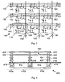
- an image sensor array 100 has an array of pixels 110.
- a pixel output 170 of each pixel 110 is connected to a first column bitline 180 and a second column bitline 190 in the respective column of pixels.
- Each row of pixels 110 is connected by a common row select 130.
- the row select 130 is activated (set to "high") by row drivers 140, the pixels 110 in that row are enabled for readout and the values of the pixels 110 are read out in parallel on to the first and second column bitline 180, 190 to readout amplifiers 150.
- Fig. 4 indicates a preferred arrangement of the invention, in that multiple bitlines are positioned one above the other. By this arrangement, the addition of one or more bitlines does not impact on the area of the photosensitive substrate and hence the pixel's sensitivity is not affected.
- a first bitline 502 and a second bitline 504 are shown connected together at regular intervals by connectors 506.
- the connectors 506 are typically connected to pixel outputs in a column of pixels. If required, only some of the connectors are connected to pixel outputs with the other connectors simply enabling connections between the first bitline 502 and the second bitline 504. It is advantageous to connect together the first and second bitlines 502, 504 at regular intervals, which adds greater redundancy to the system by mitigating the effects of multiple open-circuit defects.
Landscapes
- Engineering & Computer Science (AREA)
- Multimedia (AREA)
- Signal Processing (AREA)
- Solid State Image Pick-Up Elements (AREA)
- Transforming Light Signals Into Electric Signals (AREA)
Claims (9)
- Un capteur d'image (100) comportant une pluralité de pixels (110) disposés en lignes et en colonnes pour former une matrice de pixels,
chaque pixel (110) ayant une sortie de pixel (170),
le capteur d'image (100) comprenant au moins deux lignes de bits de colonne (180, 190) pour chaque colonne de pixels,
chaque ligne de bits de colonne (180, 190) étant connectée à chaque sortie de pixel (170) dans la colonne de pixels et à un amplificateur de lecture commun (150), caractérisé en ce que
la même sortie de pixel (170) de chaque pixel (110) est connectée aux dites deux lignes de bits de colonnes au moins (180, 190). - Un capteur d'image selon la revendication 1, dans lequel chaque ligne de bits de colonne (180, 190) est connectée à l'autre ou aux autres ligne(s) de bits de colonne (190) de la colonne respective en une pluralité de points.
- Un capteur d'image selon la revendication 1 ou la revendication 2, dans lequel au moins une ligne de bits de colonne (180, 190 ; 426, 428) d'une colonne donnée est sur un plan différent d'au moins une autre ligne de bits de colonne (180, 190 ; 426, 428) de cette colonne.
- Un capteur d'image selon la revendication 3, dans lequel la ligne de bits de colonne (180, 190 ; 426, 428) au moins est directement au-dessus de l'autre ou des autres ligne(s) de bits de colonne (180, 190 ; 426, 428).
- Un appareil de pointage optique comprenant un capteur d'image (100) selon l'une quelconque des revendications 1 à 4.
- Un dispositif de pointage optique selon la revendication 5, dans lequel le dispositif de pointage optique est une souris optique.
- Un appareil mobile comprenant un capteur d'image (100) selon l'une quelconque des revendications 1 à 4.
- Un appareil mobile selon la revendication 7, dans lequel l'appareil mobile est l'un au moins des éléments suivants : un téléphone mobile cellulaire ; un appareil photo ; un ordinateur portable ; un ordinateur de poche ; ou une webcam.
- Un appareil de détection par rayons X comprenant un capteur d'image (100) selon l'une quelconque des revendications 1 à 4.
Priority Applications (2)
| Application Number | Priority Date | Filing Date | Title |
|---|---|---|---|
| EP05253110.0A EP1725018B1 (fr) | 2005-05-19 | 2005-05-19 | Capteur de prise d'images |
| US11/419,029 US7459663B2 (en) | 2005-05-19 | 2006-05-18 | Image sensor having parallel pixel value readout |
Applications Claiming Priority (1)
| Application Number | Priority Date | Filing Date | Title |
|---|---|---|---|
| EP05253110.0A EP1725018B1 (fr) | 2005-05-19 | 2005-05-19 | Capteur de prise d'images |
Publications (2)
| Publication Number | Publication Date |
|---|---|
| EP1725018A1 EP1725018A1 (fr) | 2006-11-22 |
| EP1725018B1 true EP1725018B1 (fr) | 2013-08-28 |
Family
ID=34981411
Family Applications (1)
| Application Number | Title | Priority Date | Filing Date |
|---|---|---|---|
| EP05253110.0A Expired - Lifetime EP1725018B1 (fr) | 2005-05-19 | 2005-05-19 | Capteur de prise d'images |
Country Status (2)
| Country | Link |
|---|---|
| US (1) | US7459663B2 (fr) |
| EP (1) | EP1725018B1 (fr) |
Families Citing this family (5)
| Publication number | Priority date | Publication date | Assignee | Title |
|---|---|---|---|---|
| US8736015B2 (en) * | 2011-09-27 | 2014-05-27 | Taiwan Semiconductor Manufacturing Company, Ltd. | Integrated circuit structure and method of forming the same |
| US12526547B2 (en) | 2019-09-05 | 2026-01-13 | Waymo Llc | Smart sensor with region of interest capabilities |
| US11310451B1 (en) | 2019-09-05 | 2022-04-19 | Waymo Llc | Smart sensor with region of interest capabilities |
| US11756283B2 (en) | 2020-12-16 | 2023-09-12 | Waymo Llc | Smart sensor implementations of region of interest operating modes |
| EP4080874B1 (fr) | 2021-04-23 | 2024-12-04 | STMicroelectronics (Research & Development) Limited | Capteur de lumière |
Family Cites Families (7)
| Publication number | Priority date | Publication date | Assignee | Title |
|---|---|---|---|---|
| WO1992021204A2 (fr) | 1991-05-10 | 1992-11-26 | Eastman Kodak Company | Circuit integre a applications specifiques personnalisable a fonctions de commande et de synchronisation utilise en imagerie electronique |
| US5291293A (en) | 1992-06-01 | 1994-03-01 | Eastman Kodak Company | Electronic imaging device with defect correction |
| AU9246598A (en) | 1997-09-22 | 1999-04-12 | Interuniversitair Micro-Elektronica Centrum | Devices and methods for improving the image quality in an image sensor |
| US6215113B1 (en) | 1999-04-22 | 2001-04-10 | National Science Council | CMOS active pixel sensor |
| US6956216B2 (en) | 2000-06-15 | 2005-10-18 | Canon Kabushiki Kaisha | Semiconductor device, radiation detection device, and radiation detection system |
| US6855937B2 (en) * | 2001-05-18 | 2005-02-15 | Canon Kabushiki Kaisha | Image pickup apparatus |
| EP1301028A1 (fr) * | 2001-10-05 | 2003-04-09 | STMicroelectronics Limited | Améliorations concernant les capteurs d'images CMOS |
-
2005
- 2005-05-19 EP EP05253110.0A patent/EP1725018B1/fr not_active Expired - Lifetime
-
2006
- 2006-05-18 US US11/419,029 patent/US7459663B2/en active Active
Also Published As
| Publication number | Publication date |
|---|---|
| US7459663B2 (en) | 2008-12-02 |
| US20060261249A1 (en) | 2006-11-23 |
| EP1725018A1 (fr) | 2006-11-22 |
Similar Documents
| Publication | Publication Date | Title |
|---|---|---|
| US7034873B2 (en) | Pixel defect correction in a CMOS active pixel image sensor | |
| US20080158363A1 (en) | On-chip test system and method for active pixel sensor arrays | |
| KR101575378B1 (ko) | 고체 촬상 장치 및 이를 포함하는 x선 ct 장치 | |
| CN101431619A (zh) | 固体摄像装置及其驱动方法 | |
| KR20160003507U (ko) | 실시간 디지털 테스트 능력을 가진 이미징 시스템 | |
| JP7828961B2 (ja) | 固体撮像装置及び撮像装置 | |
| JP2005308464A (ja) | 欠陥検出装置および欠陥検出方法 | |
| EP1076453B1 (fr) | Circuit de détecteur à pixels actifs | |
| EP2076018B1 (fr) | Réseau de pixels avec une sensibilité aux défauts réduite | |
| KR20090102642A (ko) | 리소그래피용 마스크의 작성 방법, 리소그래피용 마스크 데이터의 작성 방법, 배면 입사형 고체 촬상 장치의 제조 방법, 배면 입사형 고체 촬상 장치, 및 전자 기기 | |
| KR20150110261A (ko) | 고체 촬상 장치 | |
| US7459663B2 (en) | Image sensor having parallel pixel value readout | |
| US7473881B2 (en) | Image sensor | |
| US10477201B2 (en) | Image capturing device, image capturing system, and moving body | |
| US20050271261A1 (en) | Apparatus and method for detecting defects of pattern on object | |
| US8203630B2 (en) | Method for correcting image sensor control circuitry having faulty output values and structure therefor | |
| US10484636B2 (en) | Redundancy in active pixel sensors | |
| JP7853970B2 (ja) | 固体撮像装置 | |
| TWI435151B (zh) | 陣列基板 | |
| US8249322B2 (en) | Signal line correction method and apparatus | |
| Koren et al. | A self-correcting active pixel camera | |
| CN101872774B (zh) | 固体摄像器件和摄像装置 | |
| US6396253B1 (en) | Methods and apparatus for automated repair detection of solid-state X-ray detectors | |
| JP4622009B2 (ja) | 半導体撮像装置 | |
| WO2008063495A1 (fr) | Système et procédé de suppression de rangée obscurcie pour réseaux de capteurs de pixels actifs |
Legal Events
| Date | Code | Title | Description |
|---|---|---|---|
| PUAI | Public reference made under article 153(3) epc to a published international application that has entered the european phase |
Free format text: ORIGINAL CODE: 0009012 |
|
| AK | Designated contracting states |
Kind code of ref document: A1 Designated state(s): AT BE BG CH CY CZ DE DK EE ES FI FR GB GR HU IE IS IT LI LT LU MC NL PL PT RO SE SI SK TR |
|
| AX | Request for extension of the european patent |
Extension state: AL BA HR LV MK YU |
|
| 17P | Request for examination filed |
Effective date: 20070510 |
|
| AKX | Designation fees paid |
Designated state(s): DE FR GB IT |
|
| 17Q | First examination report despatched |
Effective date: 20080917 |
|
| GRAP | Despatch of communication of intention to grant a patent |
Free format text: ORIGINAL CODE: EPIDOSNIGR1 |
|
| REG | Reference to a national code |
Ref country code: DE Ref legal event code: R079 Ref document number: 602005041026 Country of ref document: DE Free format text: PREVIOUS MAIN CLASS: H04N0003150000 Ipc: H04N0005367000 |
|
| RIC1 | Information provided on ipc code assigned before grant |
Ipc: H04N 5/367 20110101AFI20121220BHEP |
|
| GRAP | Despatch of communication of intention to grant a patent |
Free format text: ORIGINAL CODE: EPIDOSNIGR1 |
|
| INTG | Intention to grant announced |
Effective date: 20130531 |
|
| GRAS | Grant fee paid |
Free format text: ORIGINAL CODE: EPIDOSNIGR3 |
|
| GRAA | (expected) grant |
Free format text: ORIGINAL CODE: 0009210 |
|
| AK | Designated contracting states |
Kind code of ref document: B1 Designated state(s): DE FR GB IT |
|
| RAP1 | Party data changed (applicant data changed or rights of an application transferred) |
Owner name: STMICROELECTRONICS (RESEARCH & DEVELOPMENT) LIMITE |
|
| REG | Reference to a national code |
Ref country code: GB Ref legal event code: FG4D |
|
| REG | Reference to a national code |
Ref country code: DE Ref legal event code: R096 Ref document number: 602005041026 Country of ref document: DE Effective date: 20131024 |
|
| PG25 | Lapsed in a contracting state [announced via postgrant information from national office to epo] |
Ref country code: IT Free format text: LAPSE BECAUSE OF FAILURE TO SUBMIT A TRANSLATION OF THE DESCRIPTION OR TO PAY THE FEE WITHIN THE PRESCRIBED TIME-LIMIT Effective date: 20130828 |
|
| REG | Reference to a national code |
Ref country code: DE Ref legal event code: R097 Ref document number: 602005041026 Country of ref document: DE |
|
| PLBE | No opposition filed within time limit |
Free format text: ORIGINAL CODE: 0009261 |
|
| STAA | Information on the status of an ep patent application or granted ep patent |
Free format text: STATUS: NO OPPOSITION FILED WITHIN TIME LIMIT |
|
| 26N | No opposition filed |
Effective date: 20140530 |
|
| REG | Reference to a national code |
Ref country code: DE Ref legal event code: R097 Ref document number: 602005041026 Country of ref document: DE Effective date: 20140530 |
|
| REG | Reference to a national code |
Ref country code: FR Ref legal event code: PLFP Year of fee payment: 12 |
|
| REG | Reference to a national code |
Ref country code: FR Ref legal event code: PLFP Year of fee payment: 13 |
|
| REG | Reference to a national code |
Ref country code: FR Ref legal event code: PLFP Year of fee payment: 14 |
|
| REG | Reference to a national code |
Ref country code: DE Ref legal event code: R079 Ref document number: 602005041026 Country of ref document: DE Free format text: PREVIOUS MAIN CLASS: H04N0005367000 Ipc: H04N0025680000 |
|
| PGFP | Annual fee paid to national office [announced via postgrant information from national office to epo] |
Ref country code: GB Payment date: 20240418 Year of fee payment: 20 |
|
| PGFP | Annual fee paid to national office [announced via postgrant information from national office to epo] |
Ref country code: DE Payment date: 20240418 Year of fee payment: 20 |
|
| PGFP | Annual fee paid to national office [announced via postgrant information from national office to epo] |
Ref country code: FR Payment date: 20240418 Year of fee payment: 20 |
|
| REG | Reference to a national code |
Ref country code: DE Ref legal event code: R071 Ref document number: 602005041026 Country of ref document: DE |
|
| REG | Reference to a national code |
Ref country code: GB Ref legal event code: PE20 Expiry date: 20250518 |
|
| PG25 | Lapsed in a contracting state [announced via postgrant information from national office to epo] |
Ref country code: GB Free format text: LAPSE BECAUSE OF EXPIRATION OF PROTECTION Effective date: 20250518 |