EP1727210A2 - Méthode de fabrication d'un élement de fenêtre scellant un boitier et dispositif correspondant - Google Patents
Méthode de fabrication d'un élement de fenêtre scellant un boitier et dispositif correspondant Download PDFInfo
- Publication number
- EP1727210A2 EP1727210A2 EP06010607A EP06010607A EP1727210A2 EP 1727210 A2 EP1727210 A2 EP 1727210A2 EP 06010607 A EP06010607 A EP 06010607A EP 06010607 A EP06010607 A EP 06010607A EP 1727210 A2 EP1727210 A2 EP 1727210A2
- Authority
- EP
- European Patent Office
- Prior art keywords
- coating
- layer
- housing
- optical
- optical coating
- Prior art date
- Legal status (The legal status is an assumption and is not a legal conclusion. Google has not performed a legal analysis and makes no representation as to the accuracy of the status listed.)
- Granted
Links
Images

Classifications
-
- G—PHYSICS
- G01—MEASURING; TESTING
- G01J—MEASUREMENT OF INTENSITY, VELOCITY, SPECTRAL CONTENT, POLARISATION, PHASE OR PULSE CHARACTERISTICS OF INFRARED, VISIBLE OR ULTRAVIOLET LIGHT; COLORIMETRY; RADIATION PYROMETRY
- G01J5/00—Radiation pyrometry, e.g. infrared or optical thermometry
- G01J5/02—Constructional details
- G01J5/04—Casings
-
- G—PHYSICS
- G01—MEASURING; TESTING
- G01J—MEASUREMENT OF INTENSITY, VELOCITY, SPECTRAL CONTENT, POLARISATION, PHASE OR PULSE CHARACTERISTICS OF INFRARED, VISIBLE OR ULTRAVIOLET LIGHT; COLORIMETRY; RADIATION PYROMETRY
- G01J5/00—Radiation pyrometry, e.g. infrared or optical thermometry
- G01J5/02—Constructional details
- G01J5/08—Optical arrangements
- G01J5/0875—Windows; Arrangements for fastening thereof
-
- G—PHYSICS
- G01—MEASURING; TESTING
- G01J—MEASUREMENT OF INTENSITY, VELOCITY, SPECTRAL CONTENT, POLARISATION, PHASE OR PULSE CHARACTERISTICS OF INFRARED, VISIBLE OR ULTRAVIOLET LIGHT; COLORIMETRY; RADIATION PYROMETRY
- G01J5/00—Radiation pyrometry, e.g. infrared or optical thermometry
- G01J5/02—Constructional details
- G01J5/0225—Shape of the cavity itself or of elements contained in or suspended over the cavity
- G01J5/024—Special manufacturing steps or sacrificial layers or layer structures
-
- G—PHYSICS
- G01—MEASURING; TESTING
- G01J—MEASUREMENT OF INTENSITY, VELOCITY, SPECTRAL CONTENT, POLARISATION, PHASE OR PULSE CHARACTERISTICS OF INFRARED, VISIBLE OR ULTRAVIOLET LIGHT; COLORIMETRY; RADIATION PYROMETRY
- G01J5/00—Radiation pyrometry, e.g. infrared or optical thermometry
- G01J5/02—Constructional details
- G01J5/04—Casings
- G01J5/046—Materials; Selection of thermal materials
Definitions
- the invention relates to a method for producing in a housing hermetically soldered solder window elements and a housing-sealing window element.
- window elements are particularly suitable for sealing housing of radiation detectors while ensuring optical functions vacuum-tight.
- Embodiments of window elements which are soldered with the aim of a gas or vacuum-tight connection in housing of radiation detectors, are especially for infrared detectors z.
- the windows can generally be optically coated in a mask. Subsequently, a metal coating is applied to the masked areas on the surface and on the lateral edge of the window, via which the solder joint is later realized.
- the metal coating can be chemically ( JP 01-039528 ) or sputtered on ( DE 102 40 355 A1 ) become.
- An existing problem is a poor quality transition region between optical coating and metal coating.
- residues of optical layer materials can lead to adhesion problems in the region of the metal coating which impair a tight solder joint of the window with the detector housing.
- the application of the metal coating may interfere with the properties of the optical layers, e.g. B. in the form of induced adhesion problems or by scattering or Störlichteintrag at defect sites.
- the object is achieved by a method for producing window elements which can be soldered hermetically into a housing, in which optically transparent, flat carrier material (wafer) whose size is sufficient for a large number of window elements is provided with an optical coating on at least one surface is then removed from the subsequently on a coated surface frame-shaped portions which enclose optically active surfaces of the window elements, after which a coating used for producing a solder joint with the housing metal coating is applied to the generated coating-free portions and a separation of the window elements from the carrier material takes place ,
- the selective removal of the optical coating can be done by mechanical removal with limited depth of cut as well as by etching to produce the necessary adhesion to the metal coating, the mechanical removal advantageously being associated with surface roughening.
- the wafer After cleaning, the wafer is subjected to a complex coating and ablation process in which first the remaining optical coating and the coating-free subregions are completely provided with an adhesive layer system which can be selectively etched relative to the optical coating, and subsequently areas with the optical coating with a lift-off mask be covered before coating over the entire surface with a solder layer system, after which the metal coating used for the production of the solder joint with the housing results in the lift-off process, wherein the Metal coating serves as a mask for etching the adhesive layer system.
- the adhesive layer system etchable selectively to the optical coating has an interdiffusion layer consisting of aluminum and a barrier layer consisting of titanium or a titanium alloy.
- Two consecutive selective structuring processes create the possibility of introducing layers through which optical or mechanical functions can be fulfilled. These may be layers which either adjoin the optically active layer or are applied to or under the optically active layer, which have an iris or a filter function or which have an absorbing or scattering light suppressing effect.
- the approximately 30 nm thick, non-closed interdiffusion layer ensures a very high adhesive strength, since the aluminum diffuses directly through the process energy during the coating process, which preferably takes place by sputtering, into the boundary surface of the carrier material.
- the barrier layer provides an optical seal between the solder layer system and the optical coating.
- the solder layer system contains an intermediate layer consisting of platinum or iron / nickel or nickel or palladium, and a final layer consisting of gold.
- Optical layer systems which are to be used especially in the infrared spectral range can advantageously have a germanium or a zinc sulfide layer as the upper terminating layer, whereby an increase in the selectivity of the etching process of the adhesive layer system to the optical layers can be achieved.
- a wafer initially processed as an optically transparent flat carrier material as a whole ie a complex coating and Subjected to removal process and then divided into individual window elements
- they can be produced with a predetermined geometry in which it is sufficient for a vacuum-tight housing closure to produce a solder joint between an applied only on the front side of the window element metallization and the housing.
- a defect-free surface coating is achieved by sufficiently reducing noise regions which counteract good adhesion of the metal layers.
- the invention ensures very high precision in the manufacture of the Novalemia, since lithographic processes for structuring the optical and the metal coating can be used.
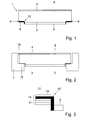
- the invention further relates to a housing-sealing window element, which has on a, provided with an optical coating window surface for making a solder connection to the housing, consisting of a base layer and a Löt Anlagensystem existing metal coating on the window surface in one of the optical coating Surface region is applied and surrounds the optical coating frame-shaped, wherein the base layer consists of an inter-diffusion layer and an overlying barrier layer, which produces an optical seal between the solder layer system and the optical coating.
- the Tempelelement 1 shown in Fig. 1 is made of an optically transmissive and advantageously designed as a wafer 2, flat support material, the size of FIG. 4 sufficient for a plurality of window elements 1.
- the one coated window surface 3 has a metal coating 8 serving to produce a soldered connection with a housing 7 (FIG. 2), which is applied on the window surface in a surface area 9 freed from the optical coating.
Landscapes
- Physics & Mathematics (AREA)
- General Physics & Mathematics (AREA)
- Spectroscopy & Molecular Physics (AREA)
- Light Receiving Elements (AREA)
- Photometry And Measurement Of Optical Pulse Characteristics (AREA)
- Casings For Electric Apparatus (AREA)
- Lasers (AREA)
- Measurement Of Radiation (AREA)
- Mounting And Adjusting Of Optical Elements (AREA)
- Led Device Packages (AREA)
- Optical Couplings Of Light Guides (AREA)
- Piezo-Electric Or Mechanical Vibrators, Or Delay Or Filter Circuits (AREA)
Applications Claiming Priority (1)
| Application Number | Priority Date | Filing Date | Title |
|---|---|---|---|
| DE102005024512A DE102005024512B3 (de) | 2005-05-26 | 2005-05-26 | Verfahren zur Herstellung von in ein Gehäuse hermetisch dicht einlötbaren Fensterelementen |
Publications (4)
| Publication Number | Publication Date |
|---|---|
| EP1727210A2 true EP1727210A2 (fr) | 2006-11-29 |
| EP1727210A3 EP1727210A3 (fr) | 2009-01-07 |
| EP1727210B1 EP1727210B1 (fr) | 2010-11-03 |
| EP1727210B8 EP1727210B8 (fr) | 2011-01-12 |
Family
ID=36992807
Family Applications (1)
| Application Number | Title | Priority Date | Filing Date |
|---|---|---|---|
| EP06010607A Not-in-force EP1727210B8 (fr) | 2005-05-26 | 2006-05-23 | Méthode de fabrication d'un élement de fenêtre scellant un boitier |
Country Status (4)
| Country | Link |
|---|---|
| US (1) | US7468293B2 (fr) |
| EP (1) | EP1727210B8 (fr) |
| AT (1) | ATE487236T1 (fr) |
| DE (2) | DE102005024512B3 (fr) |
Cited By (2)
| Publication number | Priority date | Publication date | Assignee | Title |
|---|---|---|---|---|
| WO2014183746A1 (fr) * | 2013-05-13 | 2014-11-20 | Jenoptik Optical Systems Gmbh | Procédé de fabrication d'éléments de fenêtre pouvant être brasés de manière hermétique et étanche dans un boîtier |
| EP2803961A3 (fr) * | 2013-05-14 | 2015-02-25 | Micro-Hybrid Electronic GmbH | Composant hermétique électro-optique ou opto-électronique étanche au gaz et son procédé de fabrication |
Families Citing this family (6)
| Publication number | Priority date | Publication date | Assignee | Title |
|---|---|---|---|---|
| DE102007029031A1 (de) | 2007-06-23 | 2008-12-24 | Fraunhofer-Gesellschaft zur Förderung der angewandten Forschung e.V. | Verfahren zum dauerhaften Verbinden zweier Komponenten durch Löten mit Glas- oder Metalllot |
| DE202010003402U1 (de) | 2010-03-10 | 2011-08-04 | Il-Metronic Sensortechnik Gmbh | Bauelement mit einem Gehäuse und einem Fensterelement |
| DE102015223362A1 (de) | 2015-11-25 | 2017-06-01 | Minimax Gmbh & Co. Kg | Explosionsgeschütztes Gehäuse für Mittel zum Senden und Empfangen elektromagnetischer Strahlung |
| DE102017109913A1 (de) * | 2017-05-09 | 2018-11-15 | Henke-Sass, Wolf Gmbh | Linse für ein distales Ende eines Optikkanals eines Endoskopschaftes |
| CN107104155A (zh) * | 2017-06-16 | 2017-08-29 | 苏州苏纳光电有限公司 | 探测器及其封装方法 |
| DE102021201333A1 (de) | 2020-10-27 | 2022-04-28 | Robert Bosch Gesellschaft mit beschränkter Haftung | Dichte Scheibenklebung |
Family Cites Families (9)
| Publication number | Priority date | Publication date | Assignee | Title |
|---|---|---|---|---|
| JPH0799368A (ja) * | 1993-09-29 | 1995-04-11 | Mitsubishi Electric Corp | 光半導体装置 |
| EP0734589B1 (fr) * | 1993-12-13 | 1998-03-25 | Honeywell Inc. | Microboitiers integres de silicium sous vide pour dispositifs ir |
| JP3724848B2 (ja) * | 1995-07-14 | 2005-12-07 | 則夫 岡田 | 光学用窓 |
| JPH11211555A (ja) * | 1998-01-29 | 1999-08-06 | Horiba Ltd | 赤外線検出器 |
| EP1026106A1 (fr) | 1999-02-05 | 2000-08-09 | WAM S.p.A. | Transporteur à vis pour matières en vrac |
| CA2312646A1 (fr) * | 2000-06-28 | 2001-12-28 | Institut National D'optique | Microconditionnement hybride de microdispositifs |
| US6627814B1 (en) * | 2002-03-22 | 2003-09-30 | David H. Stark | Hermetically sealed micro-device package with window |
| DE10240355B4 (de) | 2002-08-27 | 2008-01-24 | Fraunhofer-Gesellschaft zur Förderung der angewandten Forschung e.V. | Verbundbauteil und Verfahren zur Herstellung eines Verbundbauteiles |
| US6995462B2 (en) * | 2003-09-17 | 2006-02-07 | Micron Technology, Inc. | Image sensor packages |
-
2005
- 2005-05-26 DE DE102005024512A patent/DE102005024512B3/de not_active Expired - Fee Related
-
2006
- 2006-05-23 EP EP06010607A patent/EP1727210B8/fr not_active Not-in-force
- 2006-05-23 DE DE502006008207T patent/DE502006008207D1/de active Active
- 2006-05-23 AT AT06010607T patent/ATE487236T1/de active
- 2006-05-25 US US11/420,310 patent/US7468293B2/en not_active Expired - Fee Related
Cited By (6)
| Publication number | Priority date | Publication date | Assignee | Title |
|---|---|---|---|---|
| WO2014183746A1 (fr) * | 2013-05-13 | 2014-11-20 | Jenoptik Optical Systems Gmbh | Procédé de fabrication d'éléments de fenêtre pouvant être brasés de manière hermétique et étanche dans un boîtier |
| JP2016526290A (ja) * | 2013-05-13 | 2016-09-01 | イエーノプティーク オプティカル システムズ ゲーエムベーハー | 筐体内に密閉封止してはんだ付けすることができる窓要素を製造するための方法、および前記方法によって製造された自由形状窓要素 |
| US10330941B2 (en) | 2013-05-13 | 2019-06-25 | Jenoptik Optical Systems Gmbh | Method for producing window elements that can be soldered into a housing in a hermetically sealed manner and free-form window elements produced in accordance with said method |
| EP2803961A3 (fr) * | 2013-05-14 | 2015-02-25 | Micro-Hybrid Electronic GmbH | Composant hermétique électro-optique ou opto-électronique étanche au gaz et son procédé de fabrication |
| US10845047B2 (en) | 2013-05-14 | 2020-11-24 | Micro-Hybrid Electronic Gmbh | Hermetically gastight optoelectronic or electro-optical component and method for producing the same |
| EP2803961B1 (fr) | 2013-05-14 | 2024-01-17 | Micro-Hybrid Electronic GmbH | Composant hermétique électro-optique ou opto-électronique étanche au gaz et son procédé de fabrication |
Also Published As
| Publication number | Publication date |
|---|---|
| US20060268400A1 (en) | 2006-11-30 |
| EP1727210B1 (fr) | 2010-11-03 |
| EP1727210B8 (fr) | 2011-01-12 |
| EP1727210A3 (fr) | 2009-01-07 |
| ATE487236T1 (de) | 2010-11-15 |
| DE102005024512B3 (de) | 2007-02-08 |
| US7468293B2 (en) | 2008-12-23 |
| DE502006008207D1 (de) | 2010-12-16 |
Similar Documents
| Publication | Publication Date | Title |
|---|---|---|
| DE10164502B4 (de) | Verfahren zur hermetischen Verkapselung eines Bauelements | |
| EP0001220B1 (fr) | Procédé d'assemblage indirect de deux pièces | |
| WO1997020654A1 (fr) | Procede et dispositif pour appliquer sans fondant un agent a braser sur un substrat ou sur une puce | |
| EP1269450B1 (fr) | Composant pourvu d'une inscription | |
| DE102009055303B4 (de) | Verbundsubstrat und Verfahren zur Ausbildung eines Metallmusters | |
| EP1869705B1 (fr) | Procédé de fabrication de dispositifs électroniques en boîtier et dispositif électronique en boîtier | |
| DE3028044C1 (de) | Lötfähiges Schichtensystem | |
| DE102012206869A1 (de) | Mikromechanisches Bauelement und Verfahren zur Herstellung eines mikromechanischen Bauelements | |
| EP1727210B1 (fr) | Méthode de fabrication d'un élement de fenêtre scellant un boitier | |
| DE2622324C3 (de) | Verfahren zur Herstellung eines genau abgeglichenen elektrischen Netzwerkes | |
| EP1945563B1 (fr) | Composant pouvant etre employe dans des microsystemes et procede de soudage destine a la connexion de parties correspondantes de plaquette ou de composant | |
| WO2003057618A2 (fr) | Procede pour fabriquer une couverture de protection pour un composant | |
| DE19827414C2 (de) | Verfahren zum Herstellen eines Metall-Keramik-Substrates | |
| DE102008054415A1 (de) | Anordnung zweier Substrate mit einer SLID-Bondverbindung und Verfahren zur Herstellung einer solchen Anordnung | |
| EP3595802B1 (fr) | Procédé permettant de fabriquer un élément de support de membrane et élément de support de membrane servant à séparer de l'hydrogène | |
| DE102012219622B4 (de) | Mikrotechnologisches Bauelement mit Bondverbindung | |
| DE19828846C2 (de) | Verfahren zum Beschichten eines Substrats | |
| DE102008016613B4 (de) | Verfahren zur Herstellung eines elektrischen Bauelements mit mindestens einer dielektrischen Schicht und ein elektrisches Bauelement mit mindestens einer dielektrischen Schicht | |
| DE19962431A1 (de) | Verfahren zum Herstellen einer Halbleiteranordnung | |
| WO2019030040A1 (fr) | Dispositif micromécanique et procédé de fabrication correspondant | |
| DE102019212881A1 (de) | Verfahren zum Lasermikroschweißen zweier Bauteile und Bauteileverbund | |
| EP1821091B1 (fr) | Procédé de fabrication de composants électroniques et capteur de pression | |
| DE4420347A1 (de) | Verfahren und Vorrichtung zum Abgleich von elektronischen Bauelementen | |
| DE102020129380A1 (de) | Hermetisch verbundene Anordnung | |
| DE112024000670T5 (de) | Optische Komponente, transparentes Dichtungsbauteil, Substrat und Verfahren zur Herstellung einer optischen Komponente |
Legal Events
| Date | Code | Title | Description |
|---|---|---|---|
| PUAI | Public reference made under article 153(3) epc to a published international application that has entered the european phase |
Free format text: ORIGINAL CODE: 0009012 |
|
| AK | Designated contracting states |
Kind code of ref document: A2 Designated state(s): AT BE BG CH CY CZ DE DK EE ES FI FR GB GR HU IE IS IT LI LT LU LV MC NL PL PT RO SE SI SK TR |
|
| AX | Request for extension of the european patent |
Extension state: AL BA HR MK YU |
|
| PUAL | Search report despatched |
Free format text: ORIGINAL CODE: 0009013 |
|
| AK | Designated contracting states |
Kind code of ref document: A3 Designated state(s): AT BE BG CH CY CZ DE DK EE ES FI FR GB GR HU IE IS IT LI LT LU LV MC NL PL PT RO SE SI SK TR |
|
| AX | Request for extension of the european patent |
Extension state: AL BA HR MK YU |
|
| 17P | Request for examination filed |
Effective date: 20090624 |
|
| 17Q | First examination report despatched |
Effective date: 20090623 |
|
| AKX | Designation fees paid |
Designated state(s): AT BE BG CH CY CZ DE DK EE ES FI FR GB GR HU IE IS IT LI LT LU LV MC NL PL PT RO SE SI SK TR |
|
| R17C | First examination report despatched (corrected) |
Effective date: 20090723 |
|
| GRAP | Despatch of communication of intention to grant a patent |
Free format text: ORIGINAL CODE: EPIDOSNIGR1 |
|
| RTI1 | Title (correction) |
Free format text: METHOD FOR FABRICATING A WINDOW ELEMENT SEALING A HOUSING |
|
| GRAS | Grant fee paid |
Free format text: ORIGINAL CODE: EPIDOSNIGR3 |
|
| GRAA | (expected) grant |
Free format text: ORIGINAL CODE: 0009210 |
|
| AK | Designated contracting states |
Kind code of ref document: B1 Designated state(s): AT BE BG CH CY CZ DE DK EE ES FI FR GB GR HU IE IS IT LI LT LU LV MC NL PL PT RO SE SI SK TR |
|
| REG | Reference to a national code |
Ref country code: GB Ref legal event code: FG4D Free format text: NOT ENGLISH |
|
| REG | Reference to a national code |
Ref country code: CH Ref legal event code: EP |
|
| RAP2 | Party data changed (patent owner data changed or rights of a patent transferred) |
Owner name: JENOPTIK OPTICAL SYSTEMS GMBH |
|
| REG | Reference to a national code |
Ref country code: IE Ref legal event code: FG4D Free format text: LANGUAGE OF EP DOCUMENT: GERMAN |
|
| REF | Corresponds to: |
Ref document number: 502006008207 Country of ref document: DE Date of ref document: 20101216 Kind code of ref document: P |
|
| REG | Reference to a national code |
Ref country code: NL Ref legal event code: VDEP Effective date: 20101103 |
|
| LTIE | Lt: invalidation of european patent or patent extension |
Effective date: 20101103 |
|
| PG25 | Lapsed in a contracting state [announced via postgrant information from national office to epo] |
Ref country code: LT Free format text: LAPSE BECAUSE OF FAILURE TO SUBMIT A TRANSLATION OF THE DESCRIPTION OR TO PAY THE FEE WITHIN THE PRESCRIBED TIME-LIMIT Effective date: 20101103 |
|
| REG | Reference to a national code |
Ref country code: IE Ref legal event code: FD4D |
|
| PG25 | Lapsed in a contracting state [announced via postgrant information from national office to epo] |
Ref country code: SI Free format text: LAPSE BECAUSE OF FAILURE TO SUBMIT A TRANSLATION OF THE DESCRIPTION OR TO PAY THE FEE WITHIN THE PRESCRIBED TIME-LIMIT Effective date: 20101103 Ref country code: LV Free format text: LAPSE BECAUSE OF FAILURE TO SUBMIT A TRANSLATION OF THE DESCRIPTION OR TO PAY THE FEE WITHIN THE PRESCRIBED TIME-LIMIT Effective date: 20101103 Ref country code: IS Free format text: LAPSE BECAUSE OF FAILURE TO SUBMIT A TRANSLATION OF THE DESCRIPTION OR TO PAY THE FEE WITHIN THE PRESCRIBED TIME-LIMIT Effective date: 20110303 Ref country code: PT Free format text: LAPSE BECAUSE OF FAILURE TO SUBMIT A TRANSLATION OF THE DESCRIPTION OR TO PAY THE FEE WITHIN THE PRESCRIBED TIME-LIMIT Effective date: 20110303 Ref country code: BG Free format text: LAPSE BECAUSE OF FAILURE TO SUBMIT A TRANSLATION OF THE DESCRIPTION OR TO PAY THE FEE WITHIN THE PRESCRIBED TIME-LIMIT Effective date: 20110203 Ref country code: SE Free format text: LAPSE BECAUSE OF FAILURE TO SUBMIT A TRANSLATION OF THE DESCRIPTION OR TO PAY THE FEE WITHIN THE PRESCRIBED TIME-LIMIT Effective date: 20101103 Ref country code: FI Free format text: LAPSE BECAUSE OF FAILURE TO SUBMIT A TRANSLATION OF THE DESCRIPTION OR TO PAY THE FEE WITHIN THE PRESCRIBED TIME-LIMIT Effective date: 20101103 Ref country code: NL Free format text: LAPSE BECAUSE OF FAILURE TO SUBMIT A TRANSLATION OF THE DESCRIPTION OR TO PAY THE FEE WITHIN THE PRESCRIBED TIME-LIMIT Effective date: 20101103 |
|
| PG25 | Lapsed in a contracting state [announced via postgrant information from national office to epo] |
Ref country code: GR Free format text: LAPSE BECAUSE OF FAILURE TO SUBMIT A TRANSLATION OF THE DESCRIPTION OR TO PAY THE FEE WITHIN THE PRESCRIBED TIME-LIMIT Effective date: 20110204 |
|
| PG25 | Lapsed in a contracting state [announced via postgrant information from national office to epo] |
Ref country code: EE Free format text: LAPSE BECAUSE OF FAILURE TO SUBMIT A TRANSLATION OF THE DESCRIPTION OR TO PAY THE FEE WITHIN THE PRESCRIBED TIME-LIMIT Effective date: 20101103 Ref country code: IE Free format text: LAPSE BECAUSE OF FAILURE TO SUBMIT A TRANSLATION OF THE DESCRIPTION OR TO PAY THE FEE WITHIN THE PRESCRIBED TIME-LIMIT Effective date: 20101103 Ref country code: ES Free format text: LAPSE BECAUSE OF FAILURE TO SUBMIT A TRANSLATION OF THE DESCRIPTION OR TO PAY THE FEE WITHIN THE PRESCRIBED TIME-LIMIT Effective date: 20110214 Ref country code: CZ Free format text: LAPSE BECAUSE OF FAILURE TO SUBMIT A TRANSLATION OF THE DESCRIPTION OR TO PAY THE FEE WITHIN THE PRESCRIBED TIME-LIMIT Effective date: 20101103 |
|
| PG25 | Lapsed in a contracting state [announced via postgrant information from national office to epo] |
Ref country code: DK Free format text: LAPSE BECAUSE OF FAILURE TO SUBMIT A TRANSLATION OF THE DESCRIPTION OR TO PAY THE FEE WITHIN THE PRESCRIBED TIME-LIMIT Effective date: 20101103 Ref country code: SK Free format text: LAPSE BECAUSE OF FAILURE TO SUBMIT A TRANSLATION OF THE DESCRIPTION OR TO PAY THE FEE WITHIN THE PRESCRIBED TIME-LIMIT Effective date: 20101103 Ref country code: PL Free format text: LAPSE BECAUSE OF FAILURE TO SUBMIT A TRANSLATION OF THE DESCRIPTION OR TO PAY THE FEE WITHIN THE PRESCRIBED TIME-LIMIT Effective date: 20101103 Ref country code: RO Free format text: LAPSE BECAUSE OF FAILURE TO SUBMIT A TRANSLATION OF THE DESCRIPTION OR TO PAY THE FEE WITHIN THE PRESCRIBED TIME-LIMIT Effective date: 20101103 |
|
| PLBE | No opposition filed within time limit |
Free format text: ORIGINAL CODE: 0009261 |
|
| STAA | Information on the status of an ep patent application or granted ep patent |
Free format text: STATUS: NO OPPOSITION FILED WITHIN TIME LIMIT |
|
| 26N | No opposition filed |
Effective date: 20110804 |
|
| BERE | Be: lapsed |
Owner name: JENOPTIK LASER, OPTIK, SYSTEME G.M.B.H. Effective date: 20110531 |
|
| REG | Reference to a national code |
Ref country code: DE Ref legal event code: R097 Ref document number: 502006008207 Country of ref document: DE Effective date: 20110804 |
|
| PG25 | Lapsed in a contracting state [announced via postgrant information from national office to epo] |
Ref country code: IT Free format text: LAPSE BECAUSE OF FAILURE TO SUBMIT A TRANSLATION OF THE DESCRIPTION OR TO PAY THE FEE WITHIN THE PRESCRIBED TIME-LIMIT Effective date: 20101103 Ref country code: MC Free format text: LAPSE BECAUSE OF NON-PAYMENT OF DUE FEES Effective date: 20110531 |
|
| REG | Reference to a national code |
Ref country code: CH Ref legal event code: PL |
|
| PG25 | Lapsed in a contracting state [announced via postgrant information from national office to epo] |
Ref country code: CH Free format text: LAPSE BECAUSE OF NON-PAYMENT OF DUE FEES Effective date: 20110531 Ref country code: LI Free format text: LAPSE BECAUSE OF NON-PAYMENT OF DUE FEES Effective date: 20110531 |
|
| PG25 | Lapsed in a contracting state [announced via postgrant information from national office to epo] |
Ref country code: BE Free format text: LAPSE BECAUSE OF NON-PAYMENT OF DUE FEES Effective date: 20110531 |
|
| REG | Reference to a national code |
Ref country code: AT Ref legal event code: MM01 Ref document number: 487236 Country of ref document: AT Kind code of ref document: T Effective date: 20110523 |
|
| PG25 | Lapsed in a contracting state [announced via postgrant information from national office to epo] |
Ref country code: AT Free format text: LAPSE BECAUSE OF NON-PAYMENT OF DUE FEES Effective date: 20110523 |
|
| PG25 | Lapsed in a contracting state [announced via postgrant information from national office to epo] |
Ref country code: LU Free format text: LAPSE BECAUSE OF NON-PAYMENT OF DUE FEES Effective date: 20110523 Ref country code: CY Free format text: LAPSE BECAUSE OF FAILURE TO SUBMIT A TRANSLATION OF THE DESCRIPTION OR TO PAY THE FEE WITHIN THE PRESCRIBED TIME-LIMIT Effective date: 20101103 |
|
| PG25 | Lapsed in a contracting state [announced via postgrant information from national office to epo] |
Ref country code: TR Free format text: LAPSE BECAUSE OF FAILURE TO SUBMIT A TRANSLATION OF THE DESCRIPTION OR TO PAY THE FEE WITHIN THE PRESCRIBED TIME-LIMIT Effective date: 20101103 |
|
| PG25 | Lapsed in a contracting state [announced via postgrant information from national office to epo] |
Ref country code: HU Free format text: LAPSE BECAUSE OF FAILURE TO SUBMIT A TRANSLATION OF THE DESCRIPTION OR TO PAY THE FEE WITHIN THE PRESCRIBED TIME-LIMIT Effective date: 20101103 |
|
| REG | Reference to a national code |
Ref country code: FR Ref legal event code: PLFP Year of fee payment: 11 |
|
| REG | Reference to a national code |
Ref country code: FR Ref legal event code: PLFP Year of fee payment: 12 |
|
| PGFP | Annual fee paid to national office [announced via postgrant information from national office to epo] |
Ref country code: FR Payment date: 20170522 Year of fee payment: 12 Ref country code: GB Payment date: 20170524 Year of fee payment: 12 |
|
| GBPC | Gb: european patent ceased through non-payment of renewal fee |
Effective date: 20180523 |
|
| PG25 | Lapsed in a contracting state [announced via postgrant information from national office to epo] |
Ref country code: GB Free format text: LAPSE BECAUSE OF NON-PAYMENT OF DUE FEES Effective date: 20180523 Ref country code: FR Free format text: LAPSE BECAUSE OF NON-PAYMENT OF DUE FEES Effective date: 20180531 |
|
| PGFP | Annual fee paid to national office [announced via postgrant information from national office to epo] |
Ref country code: DE Payment date: 20190522 Year of fee payment: 14 |
|
| REG | Reference to a national code |
Ref country code: DE Ref legal event code: R082 Ref document number: 502006008207 Country of ref document: DE Representative=s name: GLEIM PETRI OEHMKE PATENT- UND RECHTSANWALTSPA, DE |
|
| REG | Reference to a national code |
Ref country code: DE Ref legal event code: R119 Ref document number: 502006008207 Country of ref document: DE |
|
| PG25 | Lapsed in a contracting state [announced via postgrant information from national office to epo] |
Ref country code: DE Free format text: LAPSE BECAUSE OF NON-PAYMENT OF DUE FEES Effective date: 20201201 |