EP1729302B1 - Schaltung zur Ermittlung von in Halbleiterspeicherzellen gespeicherten Daten. - Google Patents
Schaltung zur Ermittlung von in Halbleiterspeicherzellen gespeicherten Daten. Download PDFInfo
- Publication number
- EP1729302B1 EP1729302B1 EP05104656.3A EP05104656A EP1729302B1 EP 1729302 B1 EP1729302 B1 EP 1729302B1 EP 05104656 A EP05104656 A EP 05104656A EP 1729302 B1 EP1729302 B1 EP 1729302B1
- Authority
- EP
- European Patent Office
- Prior art keywords
- voltage
- memory cell
- value
- compensation
- values
- Prior art date
- Legal status (The legal status is an assumption and is not a legal conclusion. Google has not performed a legal analysis and makes no representation as to the accuracy of the status listed.)
- Expired - Lifetime
Links
Images


Classifications
-
- G—PHYSICS
- G11—INFORMATION STORAGE
- G11C—STATIC STORES
- G11C11/00—Digital stores characterised by the use of particular electric or magnetic storage elements; Storage elements therefor
- G11C11/56—Digital stores characterised by the use of particular electric or magnetic storage elements; Storage elements therefor using storage elements with more than two stable states represented by steps, e.g. of voltage, current, phase, frequency
- G11C11/5621—Digital stores characterised by the use of particular electric or magnetic storage elements; Storage elements therefor using storage elements with more than two stable states represented by steps, e.g. of voltage, current, phase, frequency using charge storage in a floating gate
- G11C11/5642—Sensing or reading circuits; Data output circuits
-
- G—PHYSICS
- G11—INFORMATION STORAGE
- G11C—STATIC STORES
- G11C7/00—Arrangements for writing information into, or reading information out from, a digital store
- G11C7/04—Arrangements for writing information into, or reading information out from, a digital store with means for avoiding disturbances due to temperature effects
-
- G—PHYSICS
- G11—INFORMATION STORAGE
- G11C—STATIC STORES
- G11C16/00—Erasable programmable read-only memories
- G11C16/02—Erasable programmable read-only memories electrically programmable
- G11C16/06—Auxiliary circuits, e.g. for writing into memory
- G11C16/30—Power supply circuits
Definitions
- the present invention generally relates to the field of integrated circuits and, particularly, to integrated circuits including non-volatile semiconductor memories, such as electrically programmable memories. More specifically, the invention relates to an improved circuit for retrieving data stored in memory cells.
- Non-volatile memories are commonly used in several applications when the data stored in the memory need to be preserved even when the power supply is off.
- the electrically programmable (and erasable) memories such as flash memories, have become very popular in applications in which the data to be stored are not immutable (as it might be, e.g., the case of a consolidated code for a microprocessor), being instead necessary from time to time to store new data, or to update the data already stored.
- the non-volatile memories include a plurality of memory cells; a typical non-volatile memory cell consists of a MOS transistor whose threshold voltage is varied for storing the desired information, for example by injecting charges into a floating gate thereof. Particularly, different program levels of the memory cells correspond to respective threshold voltage value ranges, in turn associated with respective logic values. Accordingly, the memory cells in determined biasing states are conductive or not conductive depending on the information stored therein.
- a flash memory typically includes a matrix of memory cells, and, depending on the way the memory cells in the matrix are interconnected, two classes of flash memories can be identified: those having a so-called NOR architecture, or NOR flash memories, and those having a so-called NAND architecture, shortly referred to as NAND flash memories.
- NOR architecture NOR flash memories
- NAND flash memories those having a so-called NAND architecture, shortly referred to as NAND flash memories.
- a word line, to which a selected memory cell belongs is biased to a given read voltage, typically intermediate between a first threshold voltage value, associated with a first logic value, and a second threshold voltage value, associated with a second logic value, respectively.
- the remaining word lines, controlling the other memory cells of the same string are all kept at a voltage sufficiently high to ensure that these memory cells are turned on irrespective of their program level.
- the selected memory cell is conductive only when biased at a read voltage higher than the threshold voltage thereof. Accordingly, the read voltage values are exploited for discriminating the program levels of the memory cells in reading conditions.
- the read voltages are supplied by a voltage generator included in the memory.
- the voltage generator should supply read voltages approximately located halfway between the threshold voltage values corresponding to the two adjacent program levels.
- Voltage generators known in the art are implemented and dimensioned in such a way as to supply predetermined read voltages, whose values depend on the program levels associated with the information stored in the flash memory.
- the constant trend for having very shrunk manufacturing processes determines a reduction of the read margins, which, particularly, become smaller and smaller (also of few hundreds of millivolts) in a multilevel memory.
- the threshold voltages of the memory cells are sensitive to temperature variations.
- the threshold voltages tend to decrease with an increase of temperature, and vice versa; in particular, the threshold voltage varies of an amount of the order of millivolts for degree centigrade. Accordingly, the small read margins of a multilevel memory are further reduced because of temperature variations, then increasing a probability of an incorrect reading of the memory cells.
- US2003/0189856 (Cho et al ) describes a multi-level semiconductor memory device which includes a plurality of wordlines connected to memory cells configured to store multi-level data.
- a first circuit supplies a temperature-responsive voltage to a selected word line in order to read a state of a selected memory cell.
- a second circuit supplies a pre-determined voltage to non-selected wordlines.
- the first circuit includes a semiconductor element whose resistance varies in accordance with temperature to compensate for migration of threshold voltage distribution profiles with temperature variations.
- US5864504 (Tanzawa et al ) is concerned with an electrically erasable programmable read only memory capable of reducing its margin of threshold voltage. It includes an array of memory cells that are changeable in threshold voltage for data storage of different logic levels, wherein data may be read out of any specified one of the memory cells.
- a read voltage applied to the memory cell has a temperature dependence substantially identical to that of the memory-cell threshold voltage.
- a right-verify voltage may also be designed to have the same temperature dependence as that of the memory cell. Hence the inter-threshold margin and the read margins of the memory cell can be reduced.
- EP 0 899 742 A1 discloses a circuit for generating a regulated voltage, in particular for gate terminals of non-volatile memory cells of the floating gate type, which comprises a generator circuit adapted to generate an unregulated voltage on its output, a comparator circuit coupled to the output of the generator circuit, including a reference element consisting of a non-volatile memory cell of the floating gate type and adapted to output an electric error signal tied to the difference between the unregulated voltage and the threshold voltage of the cell, and a regulator circuit coupled to the output of the comparator circuit and operative to regulate the unregulated voltage based on the value of the electric error signal.
- the regulated voltage is made programmable and tied to the parameters of the memory cell.
- the read margin can be rendered less dependent, or even essentially independent from the operating temperature by causing the voltage(s), that is (are) generated and supplied to the memory cells for retrieving data stored therein, to vary with temperature in such a way to at least partially compensate variations with the temperature of the memory cells' threshold voltage.
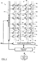
- a non-volatile semiconductor memory globally identified as 100, is illustrated, particularly an electrically-programmable, non-volatile semiconductor memory, for example a flash memory, in which the present invention is applicable.
- the flash memory 100 is integrated in a chip of semiconductor material, and includes a matrix 105 of memory cells 110, arranged in a plurality of rows and a plurality of columns.
- each memory cell 110 consists of an N-channel MOS transistor having a charge-storage element, such as a conductive floating gate adapted to be charged by injected electrons.
- a threshold voltage of the memory cell 110 can be varied, i.e., the memory cell 110 can be programmed to a given level, by injecting a given amount of charge in the floating gate thereof.
- each program level of the memory cell 110 is associated with corresponding ranges of the threshold voltage and represents a logic value stored in the memory cell 110.
- the generic memory cell 110 is capable of storing data in terms of different values taken by an electrical characteristic thereof, namely its threshold voltage.
- each memory cell 110 can be programmed to a plurality of levels, four in the example herein considered.
- a quadrilevel memory cell stores a logic value which consists of two information bits B 1 B 0 , i.e., the logic values "11", “10", “00” and "01", by convention associated with increasing values of the threshold voltage.
- the memory cell 110 when a generic memory cell 110 is selected and biased for reading its content, either for retrieving the data stored therein, or for verifying a correct completion of a program operation on the memory cell, the memory cell 110 will be conductive only if the gate-to-source biasing voltage is higher than the threshold voltage thereof.
- the flash memory 100 has, for example, a so-called NAND architecture: in the matrix 105, groups of, e.g., eight, sixteen or even more (such as thirty-two or sixty-four) memory cells 110 are connected in series to each other to form a respective memory cells string, and different memory cells strings belonging to a same matrix column are connected in parallel to each other to a same bit line BL.
- NAND architecture in the matrix 105, groups of, e.g., eight, sixteen or even more (such as thirty-two or sixty-four) memory cells 110 are connected in series to each other to form a respective memory cells string, and different memory cells strings belonging to a same matrix column are connected in parallel to each other to a same bit line BL.
- the memory cells 110 of a generic string are in particular connected in series between a source select N-channel MOS transistor 120s and a drain select N-channel MOS transistor 120d.
- a generic, intermediate memory cell 110 in the string of memory cells has the drain terminal connected to the source terminal of an adjacent memory cell 110, and the source terminal connected to the drain terminal of another adjacent memory cell 110.
- One of the two end memory cells 110 located at the ends of the string has the drain terminal connected to the source terminal of the drain select transistor 120d; the drain terminal of the drain select transistor 120d is connected to the corresponding bit line BL, as well as to the drain terminal of the corresponding drain select transistor 120d of an adjacent memory cells string.
- the other end memory cell 110 of the string has the source terminal connected to the drain terminal of the source select transistor 120s; the source terminal of the source select transistor 120s is connected to the source terminal of the corresponding source select transistor 120s of another adjacent memory cells string.
- the control gate terminals of the memory cells 110 in each matrix row are connected to a corresponding word line WL.
- the gate terminals of the drain select transistors 120d belonging to a common row of the matrix 105 are all connected to a corresponding drain select line DSL; similarly, the gate terminals of the source select transistors 120s belonging to a common row are all connected to a corresponding source select line SSL.
- the drain terminals of the drain select transistors 120d belonging to a common column of the matrix 105 are connected to a corresponding bit line BL.
- the source terminals of all the source select transistors 120s in the matrix 105 are connected to a common source line SL (which is typically kept at a reference voltage, or ground).
- the memory cells 110 belonging to a same row of the matrix 105 may be logically partitioned into memory pages. Assuming, merely by way of example, that the matrix 105 includes two memory pages for each word line WL, a first page consists for example of the memory cells 110 in an even position, and a second page consists of the memory cells 110 in an odd position.
- the flash memory 100 receives an address code ADR for selecting a desired memory page.
- a portion of the address code ADR is supplied to a row decoder/selector 125r, which selects the desired word line WL, as well as the corresponding drain select line DSL and the corresponding source select line SSL.
- Another portion of the address code ADR is supplied to a column decoder/selector 125c, which selects a desired packet of bit lines BL.
- the row decoder/selector 125r and the column decoder/selector 125c interface with read/write circuits 130 which are meant to includ all the components which are normally required for writing desired logic values into the selected memory cells 110, and for reading logic values currently stored therein.
- the read/write circuits 130 include voltage generators and boosters (such as charge pumps), and a page buffer exploited as a temporary storage during read/write operations on the memory cells 110 of the selected page.
- the read/write circuits 130 provide to the row and column decoder/selectors 125r and 125c operating voltages that take values in accordance with the specific operation to be performed on the memory cells 110, and a reference voltage (such as ground) starting from a supply voltage Vdd (for example, in a range between 2.7 V and 3.6 V) of the flash memory 100.
- a reference voltage such as ground
- the operation of the flash memory 100 is generally managed by a control unit, schematized as a block identified as 135 (for example, a microcontroller), which outputs a plurality of control signals, denoted as a whole with Sc, to be provided to corresponding blocks of the flash memory 100.
- a control unit schematized as a block identified as 135 (for example, a microcontroller), which outputs a plurality of control signals, denoted as a whole with Sc, to be provided to corresponding blocks of the flash memory 100.
- a data word to be written received from outside the memory, for example from an external microprocessor, is loaded into the page buffer of the read/write circuits 130; the data are then written in parallel into the memory cells 110 of the selected page.
- the drain select transistor 120d in the memory cell string to which the cell belongs is turned on by asserting the drain select line DSL, i.e. the row decoder/selector 125r brings this line, for example, to the supply voltage Vdd, whereas the source select transistor 120s is kept off by keeping the source select line SSL de-asserted ( e.g., grounded).
- the bit line BL, to which the memory cells string containing the memory cell 110 to be programmed is connected, is selected by the column decoder/selector 125c.
- the row decoder/selector 125r biases the word line WL, to which the selected memory cell belongs, to a relatively high program voltage, e.g. 20 V, provided by the read/write circuits 130.
- the remaining word lines WL, controlling the gates of the other memory cells 110 of the same string, are all brought to a voltage different from, particularly lower than, the program voltage applied to the selected word line WL, nonetheless sufficiently high to ensure that these memory cells 110 are turned on irrespective of their programming state, but sufficiently lower than the program voltage not to cause spurious programming (a suitable voltage is for example approximately 10 V). All the other word lines WL, associated with different memory cells strings, are for example kept grounded.
- the corresponding bit line BL is kept grounded by the column decoder/selector 125c, so that the drain select transistor 120d is surely kept on.
- the ground voltage at the bit line BL propagating through the drain select transistor 120d and the channel of the memory cells 110 in the string, reaches the channel of the memory cell 110 to be programmed; here, the voltage difference between the control gate and the channel experienced by the selected memory cell 110 is sufficient to cause electron tunneling into the floating gate.
- the drain select transistor 120d turns off as soon as the voltage of the memory cells string rises (due to the capacitive coupling) following the voltage applied to the word lines WL.
- the channels of the memory cells 110 of the selected memory cells string thus remain floating, and the string channel voltage rises to a value such that the control gate-to-channel voltage difference at the selected memory cell 110 is not sufficient to cause significant electron tunneling, and the memory cell 110 is not programmed.
- the memory cells 110 of the selected word line WL to be written into the desired logic value are programmed, while the other cells 110 are left unchanged.
- the value of the program voltage at the word line WL is usually increased step-by-step, starting from an initial value until the threshold voltage of the multilevel memory cell 110 to be programmed falls in the desired threshold voltage range, i.e. until the multilevel memory cell 110 is programmed to the level corresponding to the desired logic value.
- a program voltage pulse an amplitude thereof taking an initial voltage value, is applied to the selected word line WL and, successively, a program-verify operation is performed for verifying the completion of the program operation on the selected memory cell 110.
- the program-verify operation consists of biasing the corresponding word line WL at a predetermined program-verify voltage, provided by the read/write circuits 130; the program-verify voltage corresponds to the voltage range in which the threshold voltage of the selected memory cell 110 is intended to fall, i.e. to the logic value to be programmed into the memory cell 110. Particularly, the program-verify voltage may correspond to a lower limit of the desired threshold voltage range. In this way, if the selected memory cell 110 is seen as non-conductive when confronted with the proper program-verify voltage, the program operation is considered completed.
- a second program voltage pulse an amplitude thereof taking a value higher than the initial value, is applied to the selected word line WL and a further program-verify operation is performed.
- the program operation proceeds in this way step-by-step until the threshold voltage of the selected memory cell 110 falls in the desired voltage range, centered around a threshold voltage value corresponding to a given logic value and having the corresponding program-verify voltage as lower limit.
- the threshold voltage values are taken on an axis V.
- the erased memory cells 110 exhibit a low threshold voltage in a first voltage range centered around the threshold voltage value Vth-0, for example a negative voltage of approximately -1.5 V to -2 V.
- the memory cells 110 storing the logic value "10” exhibit a threshold voltage in a second voltage range centered around the threshold voltage value Vth-1, for example of approximately 0.6 V, higher than the threshold voltage value Vth-0, but lower than the threshold voltage value Vth-2, for example of approximately 1.9 V, which a third voltage range is centered around; the memory cells 110 showing a threshold voltage in the third voltage range stores the logic value "00".
- the memory cells 110 storing the logic value "01” exhibit a threshold voltage in a fourth voltage range centered around the threshold voltage value Vth-3, for example of approximately 3.3 V, higher than the threshold voltage values Vth-0, Vth-1 and Vth-2.
- the distance in voltage between two adjacent voltage ranges i.e. the distance between a left extreme of a generic threshold voltage range and a right extreme of the adjacent threshold voltage range, is very small, of the order of hundreds of millivolts, for example, about 600 mV.
- the program-verify voltages may correspond to the left extremes Vfy-1, Vfy-2 and Vfy-3 of the second, third and fourth voltage ranges, respectively.
- the program-verify voltages Vfy-1, Vfy-2 and Vfy-3 may take values of approximately 0.3 V, 1.6 V and 3.0 V, respectively.
- a first program pulse is applied to the memory cell, for example biasing the selected word line WL at a program voltage corresponding to the threshold voltage value Vth-2 or, more typically, by applying to the word line WL a voltage value corresponding to a first step of a predetermined voltage ramp.
- the selected word line WL is biased at the program-verify voltage Vfy-2; if the selected memory cell 110 is seen as non-conductive, then the threshold voltage thereof falls in the third threshold voltage range (corresponding to the logic value "00") and the program operation is considered completed. If the selected memory cell 110 is seen as conductive, then the program voltage is increased at a successive step, and so on.
- the drain select transistor 120d and the source select transistor 120s in the memory cells string to which the memory cell 110 belongs are turned on, by asserting the drain select line DSL and the source select line SSL (for example, these two lines are brought to the memory supply voltage Vdd by the row decoder/selector 125r ).
- the bit line BL, to which the memory cells string containing the memory cell 110 to be read is connected, is selected by the column decoder/selector 125c.
- the row decoder/selector 125r biases this word line WL in sequence to a first read voltage Vr-1 (for example, the ground voltage), intermediate between the threshold voltage value Vth-1 and the threshold voltage value Vth-0, then to a second read voltage Vr-2 (for example, equal to about 1.3 V), intermediate between the threshold voltage value Vth-2 and the threshold voltage value Vth-1, and then to a third read voltage Vr-3 (for example, equal to about 2.7 V), intermediate between the threshold voltage value Vth-3 and the threshold voltage value Vth-2.
- Vr-1 for example, the ground voltage
- Vr-2 for example, equal to about 1.3 V
- Vr-3 for example, equal to about 2.7 V
- the read voltage values Vr-i are preferably chosen so as to fall halfway between two adjacent threshold voltage distributions, i.e. equal to the mean point in the voltage distance between two adjacent distributions.
- This solution allows to optimize read voltage margins between the read voltage value Vr-i and the right extreme of the distribution centered around the threshold voltage value Vth-(i-1), and between the read voltage value Vr-i and the left extreme of the distribution centered around the threshold voltage value Vth-i; these read margins are typically very small in a multilevel memory, and for example of about 300 mV.
- the remaining word lines WL controlling the gates of the other memory cells 110 of the same string, are all kept to a voltage (for example, a voltage of approximately 5 V) sufficiently high to ensure that these memory cells 110 are turned on irrespective of their program level. All the other word lines WL, associated with different memory cells strings, are for example kept grounded.
- the read/write circuits 130 When the selected memory cell 110 is conductive, the read/write circuits 130 read, for example, a high logic value "1" at the corresponding selected bit line BL; on the contrary, when the selected memory cell 110 is not conductive, the read/write circuits 130 read, for example, a low logic value "0".
- the read/write circuits 130 By applying in sequence the three different read voltages Vr-1, Vr-2 and Vr-3 to the selected word line WL, three respective logic values are read in sequence at the corresponding selected bit line BL by the read/write circuits 130. This sequence of three logic values "1” or "0" is decoded by the read/write circuits 130 as a combination corresponding to the two information bits B 1 B 0 stored in the selected memory cell 110.
- the memory cells' threshold voltages, and thus the threshold voltage distributions of the memory cells 110 are sensitive to temperature variations; in particular, the threshold voltages tend to decrease with an increase of temperature, and vice versa.
- the threshold voltage distributions are shown for three different temperature values T of 90°C, 27°C and -40°C.
- T the threshold voltage distributions at 27°C
- a typical temperature under normal operating conditions are drawn in solid line.
- the threshold voltage distributions at -40°C are drawn in dashed line and shifted to the right of the threshold voltage distributions at 27°C, i.e. towards higher threshold voltage values.
- the threshold voltage distributions at 90°C are drawn in dashed-and-dot line and shifted to the left of the threshold voltage distributions at 27°C, i.e. towards lower threshold voltage values.
- the threshold voltage of a memory cell 110 shifts of an amount of the order of millivolts for degree centigrade, for example of about -1.5 mV/°C; the sign "-" means that for an increase of temperature the threshold voltage decreases, whereas for a decrease of temperature the threshold voltage increases.
- the read voltages Vr-1, Vr-2 and Vr-3, generated by a voltage generator included in the read/write circuits 130 need to shift in accordance with the threshold voltage of the memory cell 110.
- the shift of the threshold voltage is, for example, of about 100 mV in a temperature range between -40°C and 90°C with variations of -1.5 mV/°C, i.e. a value of approximately one third of the read margins.
- program-verify voltages Vfy-1, Vfy-2 and Vfy-3 need to shift in accordance with temperature translations, so that the extremes of the threshold distributions are positioned at a substantially fixed distance from the read voltages Vr-1, Vr-2 and Vr-3.
- a voltage generator 300 included in the read/write circuits 130 and according to an embodiment of the present invention, is shown.
- the voltage generator 300 generates an operating voltage Vo, adapted to be used as a biasing voltage for the memory cells 110 for accessing them and retrieving the data stored therein.
- the voltage Vo generated by the voltage generator 300 takes values variable with the temperature, in a way tracking the threshold voltages of the memory cells, starting from a reference voltage Vbg which is very stable with the temperature.
- the voltage generator 300 includes a voltage regulator 305, which comprises an operational amplifier 310, receiving as voltage supplies the ground and the supply voltage Vdd.
- the operational amplifier 310 receives, at an inverting input terminal "-" thereof, the reference voltage Vbg, supplied thereto by a reference voltage generator 315 included in the read/write circuits 130.
- the reference voltage generator 315 includes a band-gap reference voltage generator, capable of providing a band-gap reference voltage Vbg which is very stable, particularly against operating temperature variations.
- the voltage regulator 305 further includes a p-MOS transistor Mr having the source terminal receiving the supply voltage Vdd, and having a gate terminal connected to an output terminal of the operational amplifier 310, said output terminal supplying a drive voltage Vd.
- the voltage regulator 305 further includes a voltage divider 320; the voltage divider 320 in turn comprises a series of, in the example, seven resistors R10, R11, R12, R13, R14, R15 and R16 connected one to another between the drain terminal of the transistor Mr and the ground. Particularly, in the resistor series the resistor R10 has a first terminal coupled to the drain terminal of the transistor Mr and the resistor R16 has a first terminal coupled to ground.
- the operational amplifier 310 is coupled in negative feed-back to the voltage divider 320 by having a non-inverting input terminal "+" coupled to respective first terminals of the resistors R13 and R14 connected together.
- the voltage regulator 305 is adapted to cause the terminals of the resistors R10, R11, R12, R13, R14, R15 and R16 to reach each one a respective prescribed, regulated voltage, depending on the resistors' resistances, and on the values of the reference voltage Vbg and of the supply voltage Vdd.
- the resistors R10, R11, R12, R13, R14, R15 and R16 are dimensioned so that, in operation, a regulated voltage Vfyin-3 at the first terminal of the resistor R10, which is coupled to the drain terminal of the transistor Mr, supplying a regulated voltage, corresponds the program-verify voltage Vfy-3 associated with the logic value "01"; a regulated voltage Vrin-3 at the common terminals of the resistors R11 and R12 corresponds to the read voltage Vr-3 exploited for discriminating the logic values "01” and "00”; a regulated voltage Vfyin-2 at the common terminals of the resistors R12 and R13 corresponds to the program-verify voltage Vfy-2 associated with the logic value "00"; a regulated voltage Vrin-2 at the common terminals of the resistors R14 and R15, corresponds to the read voltage Vr-2 exploited for discriminating the logic values "10" and "00”; a regulated voltage Vfyin-1
- the voltage divider 320 further includes five switches SW-1, SW-2, SW-3, SW-4 and SW-5, for example consisting each one of a pass gate.
- the switch SW-1 has a first terminal connected to the first terminal of the resistor R10 and to the drain terminal of the transistor Mr, supplying the regulated voltage Vfyin-3.
- the switch SW-2 has a first terminal connected to the common terminals of the resistors R11 and R12, supplying the regulated voltage Vrin-3.
- the switch SW-3 has a first terminal connected to the common terminals of the resistors R12 and R13, supplying the regulated voltage Vfyin-2.
- the switch SW-4 has a first terminal connected to the common terminals of the resistor R14 and R15, supplying the regulated voltage Vrin-2.
- the switch SW-5 has a first terminal connected to the common second terminals of the resistors R15 and R16, supplying the regulated voltage Vfyin-1.
- the switches SW-1, SW-2, SW-3, SW-4 and SW-5 have respective second terminals connected together, whereat a regulated output voltage Vreg, which is very stable in temperature, being derived by the band-gap reference voltage Vbg, is provided.
- Each switch SW-1, SW-2, SW-3, SW-4, SW-5 is controlled by a respective enabling signal EN-1, EN-2, EN-3, EN-4, EN-5 provided for example by the control unit 135, which enables one switch SW-1, SW-2, SW-3, SW-4, SW-5 at time in accordance with the desired operation to be performed on the flash memory 100.
- the regulated output voltage Vreg takes a desired value equal to a selected one among the regulated voltages Vfyin-1, Vfyin-2, Vfyin-3, Vrin-2 or Vrin-3.
- the voltage divider 320 further supplies a regulated gate control voltage Vg to a gate terminal of an n-MOS transistor Mt included in the voltage generator 300 according to an embodiment of the present invention.
- the regulated gate control voltage Vg is taken at the common terminals of the resistors R10 and R11.
- the n-MOS transistor Mt has the drain terminal receiving the supply voltage Vdd and the source terminal connected to a first terminal of a source resistor Rs, a second terminal thereof being connected to ground.
- the source resistor Rs has a relatively high resistance, for example of hundreds of kiloohms, in order to limit a current sunk by the n-MOS transistor Mt to a desired small value, for example of the order of microamperes.
- the voltage generator 300 further comprises a buffer 325 consisting of an operational amplifier supplied between the supply voltage Vdd and the ground and having a non-inverting input terminal "+" receiving the source voltage Vs and an inverting input terminal "-" feed-back connected to an output terminal thereof. Accordingly, a buffered voltage Vs' supplied at the output terminal of the buffer 325 is equal to the source voltage Vs.
- a further operational amplifier 330 has an inverting input terminal "-" coupled to the output terminal of the buffer 325 by means of a first resistor R1, having a first terminal connected to the output terminal of the buffer 325 and a second terminal connected to the inverting input terminal "-".
- a non-inverting input terminal "+" of the operational amplifier 330 receives the regulated output voltage Vreg supplied by the voltage regulator 305.
- the operational amplifier 330 is supplied between a bootstrapped voltage Vpp, higher than the supply voltage Vdd and supplied, for example, by a charge pump of the read/write circuits 130 (not shown in the drawing) and the ground.
- the operational amplifier 330 has an output terminal coupled in negative feed-back to the inverting input terminal "-" thereof by means of a second resistor R2, having a first terminal connected to the inverting input terminal "-" and a second terminal coupled to the output terminal.
- the transistor Mt, the resistor Rs and the buffer 325 form a compensation voltage generator generating a compensation voltage Vs' having a prescribed temperature dependency.
- the resistors R1 and R2, and the operation amplifier 330 form a voltage combining circuit, combining the voltage Vreg and the compensation voltage Vs', thereby imparting to the voltage Vo a desired temperature dependency.
- Vs Vg ⁇ Vgs
- Vo Vreg + R 2 R 1 Vreg ⁇ Vg + Vgs
- the value of the operating voltage Vo depends on the two voltages Vreg and Vg, which are both very stable in temperature, and on the gate-source voltage Vgs of the transistor Mt, which instead varies with temperature, particularly in the same way as the threshold voltage of the memory cells does.
- the operating voltage Vo varies with temperature in the same way as the threshold voltage of the memory cells 110.
- the drive gate voltage Vg takes a prescribed value, for example, 1.8 V (the value of the voltage Vg is for example chosen depending on the threshold voltage of the transistor Mt ).
- the voltage regulator 305 providing the regulated voltage Vreg in a range between 0.7 V and 2.0 V, needs not be supplied by a bootstrapped voltage. Also, by supplying the amplifier 330 between the voltage Vpp and a negative voltage lower than the ground voltage, negative output voltage values exhibiting the desired dependency with temperature can be obtained.
- the operating voltage Vo, the drive gate voltage Vg and the buffered voltage Vs' vs. the regulated voltage Vreg are shown, obtained by a simulation of the operation of a NAND flash memory including a voltage generator according to an embodiment of the present invention.
- the regulated voltage Vreg is varied between 0.7 V and 2.1 V
- the threshold voltage Vth of the transistor Mt varies with the temperature, accordingly varying the buffered, compensation voltage Vs'.
- the voltages at a temperature of 27°C are shown in continuous line, at -40°C in dashed line and at 90°C in dash-and-dot line.
- the specific value of the threshold voltage Vth of the transistor Mt depends on the specific technology adopted; a typical value of the threshold voltage Vt may be of 0.45 V at a temperature of 27°C, of about 0.35 V at 90°C and of about 0.55 V at -40°C; accordingly, the buffered voltage Vs' takes the value of 1.1 V at 27°C, the value of 1.2 V at 90°C and the value of 1.0 V at - 40°C.
- the operating voltage Vo shifts in the direction of the axis of the ordinates V with temperature variations, tracking the threshold voltage of the memory cells.
- the operation voltage Vo continuously line
- the operation voltage Vo varies between 0.3 V and about 3.0 V
- at -40°C dashed line
- it varies between about 0.4 V and about 3.1 V
- 90°C dashed line
- it varies between about 0.2 V and about 2.9 V, decreasing with respect the operation voltage Vo at 27°C.
- the voltage generator according to the present invention ensures optimized read margins also in case of great temperature variations (for example, from 27°C to 90°C); in fact, the operating voltage Vo varies in accordance with the threshold voltage of the memory cells.
- This temperature compensation is very advantageous in memories with high density, such as the multilevel memories, and in memories manufactured by very shrunk processes, which have read margins greatly reduced. Accordingly, a probability of an incorrect reading of the memory cells is decreased.
- the semiconductor memory can be different from a flash memory, the matrix of memory cells can be arranged in a way different from a NAND architecture and the memory cells can be not multilevel.
- the memory can include a plurality of voltage generators according to the present invention.
- the voltage generator can receive a reference voltage from a reference voltage generator different from a band gap generator and the voltage regulator can be implement in a different way; particularly, the voltage divider can be different from a series of resistors.
Landscapes
- Engineering & Computer Science (AREA)
- Computer Hardware Design (AREA)
- Read Only Memory (AREA)
Claims (9)
- Schaltung, die Folgendes umfasst: mindestens eine Speicherzelle (110), die dazu angepasst ist, vorbestimmten Schwellenspannungswerten entsprechende Daten zu speichern, wobei die Schwellenspannungswerte von einer Veränderlichkeit mit der Temperatur gemäß einem ersten Änderungsgesetz betroffen sind, und einen Spannungserzeuger (300), der dazu angepasst ist, eine der mindestens einen Speicherzelle (110) zuzuführende Betriebsspannung (Vo) zum Auslesen der darin gespeicherten Daten zu erzeugen, wobei der Spannungserzeuger ein erstes Mittel (305) umfasst, das dazu angepasst ist, zu bewirken, dass die erzeugte Betriebsspannung abhängig von einer an der Speicherzelle auszuführenden Operation einen Wert in einer mindestens einen Sollwert (Vr-1, Vr-2, Vr-3, Vfy-1, Vfy-2, Vfy-3) umfassenden Menge von Sollwerten annimmt,wobei der Spannungserzeuger weiter ein zweites Mittel (Mt, Rs, 325, R1, R2, 330) umfasst, um zu bewirken, dass der von der erzeugten Betriebsspannung angenommene Wert sich gemäß einem vorgegebenen zweiten Änderungsgesetz mit der Temperatur ändert, wobei das zweite Mittel ein Ausgleichsschaltungselement (Mt) umfasst, das die elektrische Charakteristik aufweist, die ausgenutzt wird, um die Änderung des von der erzeugten Betriebsspannung angenommenen Werts zu bewirken, wobeidas Ausgleichsschaltungselement ein MOS-Transistorelement (Mt) mit veränderlicher Leitfähigkeit umfasst, das eine Schwellenspannung aufweist, die eine Veränderlichkeit mit der Temperatur zeigt, die derjenigen der Schwellenspannung eines die Speicherzelle bildenden MOS-Transistors entspricht, wobei das Element mit veränderlicher Leitfähigkeit einen Gate-Anschluss, der eine Steuerspannung von dem ersten Mittel empfängt, und einen Stromzufuhranschluss zum Zuführen eines Stroms mit einem von der Steuerspannung und deren Schwellenspannung abhängigen Wert aufweist,das erste Mittel einen Spannungsregler (310, Mr, R10 - R16) umfasst, der dazu angepasst ist, eine geregelte Spannung (Vreg) zu erzeugen, die einen Wert in der Menge von Sollwerten annimmt, wobei die geregelte Spannung gegenüber Temperaturänderungen stabil ist; unddas zweite Mittel Folgendes umfasst:ein Ausgleichsspannungserzeugermittel (Mt, Rs, 325), das dazu angepasst ist, eine Ausgleichsspannung (Vs') zu erzeugen, die sich gemäß dem zweiten Änderungsgesetz mit der Temperatur ändert, wobei das Ausgleichsspannungserzeugermittel das Ausgleichsschaltungselement umfasst; undein Spannungskombinationsmittel (R1, R2, 330), das die geregelte Spannung und die Ausgleichsspannung empfängt und dazu angepasst ist, die geregelte Spannung und die Ausgleichsspannung zu kombinieren, um die Betriebsspannung zu erhalten;wobei das zweite Änderungsgesetz derart ist, dass die Änderung der Ausgleichsspannung mit der Temperatur proportional zu der Änderung mit der Temperatur der Schwellenspannung des MOS-Transistors mit veränderlicher Leitfähigkeit ist; unddas Spannungskombinationsmittel dazu angepasst ist, die geregelte Temperatur auf derartige Weise mit der Ausgleichsspannung zu kombinieren, dass die Änderung der Betriebsspannung mit der Temperatur proportional zu der Änderung der Schwellenspannung mit der Temperatur des MOS-Transistors mit veränderlicher Leitfähigkeit ist;wobei das Ausgleichsspannungserzeugermittel weiter einen Strom/Spannungswandler (Rs, 325) umfasst, der an den Stromzufuhranschluss gekoppelt ist, um den zugeführten Strom in die Ausgleichsspannung umzuwandeln.
- Schaltung nach Anspruch 1, wobei die Menge von Sollwerten mindestens einen ersten Lesewert, der in einer Speicherzellen-Leseoperation zum Lesen der in der mindestens einen Speicherzelle gespeicherten Daten verwendet wird, und mindestens einen zweiten Lesewert, der in einer Datenprogramm-Verifizierungsoperation zum Verifizieren von in der Speicherzelle programmierten Daten verwendet wird, umfasst.
- Schaltung nach Anspruch 1, wobei die Steuerspannung von dem Spannungsregler erzeugt wird.
- Schaltung nach Anspruch 3, wobei das Spannungskombinationsmittel eine Spannungssummierungsstufe (R1, R2, 330) umfasst, die die geregelte Spannung und die Ausgleichsspannung empfängt und aufsummiert.
- Schaltung nach Anspruch 4, wobei die Spannungssummierungsstufe Folgendes umfasst:einen Operationsverstärker (330) mit einem ersten Eingangsanschluss ("+"), der die geregelte Spannung empfängt, einem zweiten Eingangsanschluss ("-"), der die Ausgleichsspannung empfängt, und einem Ausgangsanschluss, der die Betriebsspannung bereitstellt, undeinen Rückkopplungszweig (R1, R2) mit einem ersten Knoten zum Empfangen der Ausgleichsspannung, einem an den zweiten Eingangsanschluss gekoppelten zweiten Knoten zum Zuführen der Ausgleichsspannung und einem dritten Knoten zum Rückkoppeln des Ausgangsanschlusses an den zweiten Eingangsanschluss.
- Schaltung nach einem der vorangehenden Ansprüche, wobei der Spannungsregler Folgendes umfasst:einen Differentialverstärker (310) mit einem ersten Eingangsanschluss ("+") zum Empfangen einer Bezugsspannung (Vbg), einem zweiten Eingangsanschluss ("-") zum Empfangen einer Rückkopplungsspannung und einem Treiberanschluss zum Bereitstellen einer Treiberspannung (Vd), die einem Vergleich zwischen der Bezugsspannung und der Rückkopplungsspannung entspricht; undein Rückkopplungsnetz (Mr, R10 - R16, SW-1 - SW-5) zum Rückkoppeln des Treiberanschlusses und des zweiten Eingangsanschlusses des Differentialverstärkers, wobei das Rückkopplungsnetz Folgendes umfasst:einen Spannungsteiler (R10 - R16, SW-1 - SW-5) mit einem Rückkopplungsknoten zum Bereitstellen der Rückkopplungsspannung, einem Ausgangsknoten zum Bereitstellen der geregelten Spannung und einem weiteren Transistorelement (Mr) mit veränderlicher Leitfähigkeit, das an den Spannungsteiler gekoppelt ist und von der Treiberspannung gesteuert wird, um die geregelte Spannung zu regeln.
- Schaltung nach Anspruch 6, wobei das Rückkopplungsnetz weiter ein Schaltmittel (SW-1 - SW-5) umfasst, das an den Spannungsteiler gekoppelt ist, um zu bewirken, dass der Wert der geregelten Spannung selektiv einen Wert in der Menge von Sollwerten annimmt.
- Schaltung nach einem der Ansprüche 2 bis 7, wobei es sich bei der mindestens einen MOS-Speicherzelle um eine mehrstufige Speicherzelle handelt, die dazu angepasst ist, mehr als ein Bit umfassende Daten zu speichern, indem sie unterschiedliche Bereiche von Werten der Schwellenspannungswerte jeweiligen Logikwerten zuordnet, wobei der mindestens eine erste Wert der Betriebsspannung eine Vielzahl von ersten Werten umfasst und der zweite Wert der erzeugten Betriebsspannung eine Vielzahl von zweiten Werten umfasst.
- Schaltung nach einem der vorangehenden Ansprüche, wobei eine Vielzahl der mindestens einen MOS-Speicherzellen (110) in einer Matrix (105) mit einer NAND-Architektur angeordnet ist.
Priority Applications (3)
| Application Number | Priority Date | Filing Date | Title |
|---|---|---|---|
| EP05104656.3A EP1729302B1 (de) | 2005-05-31 | 2005-05-31 | Schaltung zur Ermittlung von in Halbleiterspeicherzellen gespeicherten Daten. |
| US11/444,892 US7474577B2 (en) | 2005-05-31 | 2006-05-31 | Circuit and method for retrieving data stored in semiconductor memory cells |
| US12/248,843 US7889586B2 (en) | 2005-05-31 | 2008-10-09 | Circuit and method for retrieving data stored in semiconductor memory cells |
Applications Claiming Priority (1)
| Application Number | Priority Date | Filing Date | Title |
|---|---|---|---|
| EP05104656.3A EP1729302B1 (de) | 2005-05-31 | 2005-05-31 | Schaltung zur Ermittlung von in Halbleiterspeicherzellen gespeicherten Daten. |
Publications (2)
| Publication Number | Publication Date |
|---|---|
| EP1729302A1 EP1729302A1 (de) | 2006-12-06 |
| EP1729302B1 true EP1729302B1 (de) | 2019-01-02 |
Family
ID=34940024
Family Applications (1)
| Application Number | Title | Priority Date | Filing Date |
|---|---|---|---|
| EP05104656.3A Expired - Lifetime EP1729302B1 (de) | 2005-05-31 | 2005-05-31 | Schaltung zur Ermittlung von in Halbleiterspeicherzellen gespeicherten Daten. |
Country Status (2)
| Country | Link |
|---|---|
| US (2) | US7474577B2 (de) |
| EP (1) | EP1729302B1 (de) |
Families Citing this family (24)
| Publication number | Priority date | Publication date | Assignee | Title |
|---|---|---|---|---|
| EP1729302B1 (de) | 2005-05-31 | 2019-01-02 | Micron Technology, Inc. | Schaltung zur Ermittlung von in Halbleiterspeicherzellen gespeicherten Daten. |
| US7586795B2 (en) | 2006-03-20 | 2009-09-08 | Cypress Semiconductor Corporation | Variable reference voltage circuit for non-volatile memory |
| US7391650B2 (en) * | 2006-06-16 | 2008-06-24 | Sandisk Corporation | Method for operating non-volatile memory using temperature compensation of voltages of unselected word lines and select gates |
| US7460415B2 (en) * | 2006-12-15 | 2008-12-02 | Spansion Llc | Drain voltage regulator |
| US8125243B1 (en) * | 2007-03-12 | 2012-02-28 | Cypress Semiconductor Corporation | Integrity checking of configurable data of programmable device |
| US7800951B2 (en) * | 2007-08-20 | 2010-09-21 | Marvell World Trade Ltd. | Threshold voltage digitizer for array of programmable threshold transistors |
| KR100927782B1 (ko) * | 2008-05-20 | 2009-11-20 | 주식회사 하이닉스반도체 | 불휘발성 메모리 장치의 독출/검증 기준전압 공급부 |
| KR101434400B1 (ko) * | 2008-07-09 | 2014-08-27 | 삼성전자주식회사 | 불휘발성 메모리 장치 및 메모리 시스템 및 그것의 관리방법 |
| US7978529B1 (en) * | 2008-12-24 | 2011-07-12 | Micron Technology, Inc. | Rewritable single-bit-per-cell flash memory |
| KR20100101798A (ko) * | 2009-03-10 | 2010-09-20 | 삼성전자주식회사 | 메모리 장치의 프로그램 방법 및 이를 위한 메모리 장치 |
| JP2011028827A (ja) * | 2009-06-25 | 2011-02-10 | Toshiba Corp | 半導体記憶装置 |
| US9209749B2 (en) * | 2012-12-10 | 2015-12-08 | Samsung Electronics Co., Ltd. | Multiplier circuit and wireless communication apparatus using the same |
| KR102140783B1 (ko) * | 2013-06-17 | 2020-08-04 | 삼성전자주식회사 | 반도체 메모리 장치 및 반도체 패키지 |
| US9349474B2 (en) * | 2013-06-21 | 2016-05-24 | Micron Technology, Inc. | Apparatuses and methods for limiting string current in a memory |
| GB201418888D0 (en) * | 2014-10-23 | 2014-12-10 | Univ Lancaster | Improvements relating to electronic memory devices |
| CN104793685B (zh) * | 2015-04-17 | 2016-06-29 | 上海华虹宏力半导体制造有限公司 | 基准电压产生电路 |
| TWI567742B (zh) * | 2015-04-23 | 2017-01-21 | 旺宏電子股份有限公司 | 電子裝置及非揮發性記憶體裝置與編程方法 |
| KR20160148788A (ko) * | 2015-06-16 | 2016-12-27 | 에스케이하이닉스 주식회사 | 반도체장치 및 반도체시스템 |
| KR102659596B1 (ko) * | 2016-08-26 | 2024-04-19 | 삼성전자주식회사 | 비휘발성 메모리 장치 |
| JP2019164850A (ja) * | 2018-03-19 | 2019-09-26 | 東芝メモリ株式会社 | メモリシステム |
| US10424385B1 (en) * | 2018-08-28 | 2019-09-24 | Dell Products L. P. | Self-configuring integrated circuit device |
| US10546641B1 (en) | 2018-12-07 | 2020-01-28 | Micron Technology, Inc. | Memory devices with controlled wordline ramp rates, and associated systems and methods |
| US11874736B2 (en) * | 2021-08-11 | 2024-01-16 | Apple Inc. | Calculating soft metrics depending on threshold voltages of memory cells in multiple neighbor word lines |
| US12158806B1 (en) | 2023-06-27 | 2024-12-03 | Apple Inc. | Efficient estimation of threshold voltage distributions in a nonvolatile memory |
Citations (1)
| Publication number | Priority date | Publication date | Assignee | Title |
|---|---|---|---|---|
| EP0899742A1 (de) * | 1997-08-29 | 1999-03-03 | STMicroelectronics S.r.l. | Verfahren und Schaltung zur Erzeugung einer Gatterspannung für nichtfluchtige Speicheranordnungen |
Family Cites Families (10)
| Publication number | Priority date | Publication date | Assignee | Title |
|---|---|---|---|---|
| JP3648304B2 (ja) | 1995-11-17 | 2005-05-18 | 株式会社東芝 | 不揮発性半導体記憶装置 |
| JP3954245B2 (ja) * | 1999-07-22 | 2007-08-08 | 株式会社東芝 | 電圧発生回路 |
| DE60129928D1 (de) * | 2001-04-19 | 2007-09-27 | St Microelectronics Srl | Verfahren und Schaltung zur Zeitsteuerung des dynamischen Auslesens einer Speicherzelle mit Kontrolle der Integrationszeit |
| KR100476888B1 (ko) | 2002-04-04 | 2005-03-17 | 삼성전자주식회사 | 온도보상기능을 가진 멀티비트 플래쉬메모리 |
| US6809978B2 (en) * | 2002-05-13 | 2004-10-26 | Infineon Technologies Ag | Implementation of a temperature sensor to control internal chip voltages |
| US6898104B2 (en) * | 2002-11-12 | 2005-05-24 | Kabushiki Kaisha Toshiba | Semiconductor device having semiconductor memory with sense amplifier |
| US6868025B2 (en) * | 2003-03-10 | 2005-03-15 | Sharp Laboratories Of America, Inc. | Temperature compensated RRAM circuit |
| JP2005285197A (ja) * | 2004-03-29 | 2005-10-13 | Renesas Technology Corp | 半導体記憶装置 |
| EP1729302B1 (de) | 2005-05-31 | 2019-01-02 | Micron Technology, Inc. | Schaltung zur Ermittlung von in Halbleiterspeicherzellen gespeicherten Daten. |
| US7518930B2 (en) * | 2006-04-21 | 2009-04-14 | Sandisk Corporation | Method for generating and adjusting selected word line voltage |
-
2005
- 2005-05-31 EP EP05104656.3A patent/EP1729302B1/de not_active Expired - Lifetime
-
2006
- 2006-05-31 US US11/444,892 patent/US7474577B2/en active Active
-
2008
- 2008-10-09 US US12/248,843 patent/US7889586B2/en active Active
Patent Citations (1)
| Publication number | Priority date | Publication date | Assignee | Title |
|---|---|---|---|---|
| EP0899742A1 (de) * | 1997-08-29 | 1999-03-03 | STMicroelectronics S.r.l. | Verfahren und Schaltung zur Erzeugung einer Gatterspannung für nichtfluchtige Speicheranordnungen |
Also Published As
| Publication number | Publication date |
|---|---|
| US20060291322A1 (en) | 2006-12-28 |
| US7474577B2 (en) | 2009-01-06 |
| EP1729302A1 (de) | 2006-12-06 |
| US7889586B2 (en) | 2011-02-15 |
| US20090262593A1 (en) | 2009-10-22 |
Similar Documents
| Publication | Publication Date | Title |
|---|---|---|
| US7889586B2 (en) | Circuit and method for retrieving data stored in semiconductor memory cells | |
| EP1620860B1 (de) | Speicher mit gleichförmiger lese- und verifikationsschwelle | |
| US5712815A (en) | Multiple bits per-cell flash EEPROM capable of concurrently programming and verifying memory cells and reference cells | |
| KR100496866B1 (ko) | 미프로그램된 셀들 및 과프로그램된 셀들 없이 균일한문턱 전압 분포를 갖는 플레쉬 메모리 장치 및 그프로그램 검증 방법 | |
| US6714455B2 (en) | Memory apparatus including programmable non-volatile multi-bit memory cell, and apparatus and method for demarcating memory states of the cell | |
| JP3652826B2 (ja) | 多値記憶不揮発性半導体メモリ | |
| KR100303549B1 (ko) | 비휘발성메모리셀당복수의디지털비트를저장및검색하기위한집적회로 | |
| US7002869B2 (en) | Voltage regulator circuit | |
| US7558117B2 (en) | Nonvolatile semiconductor memory device | |
| KR20010032309A (ko) | 프로그램 가능 비휘발성 다-비트 메모리 셀을 포함한메모리 장치와 셀의 메모리 상태 구분용 장치 및 방법 | |
| KR100521364B1 (ko) | 플레쉬 메모리 셀들의 프로그램 오판을 방지하고 균일한문턱 전압 산포를 가질 수 있는 플레쉬 메모리 장치 및 그프로그램 검증 방법 | |
| KR20030079425A (ko) | 온도보상기능을 가진 멀티비트 플래쉬메모리 | |
| US6101125A (en) | Electrically programmable memory and method of programming | |
| US6281665B1 (en) | High speed internal voltage generator with reduced current draw | |
| US7460402B2 (en) | Semiconductor memory device which generates voltages corresponding to a plurality of threshold voltages | |
| US7952935B2 (en) | Nonvolatile memory device and program or verification method using the same | |
| US7872918B2 (en) | Nonvolatile memory device and program or erase method using the same | |
| US7173860B2 (en) | Source controlled operation of non-volatile memories | |
| US7372747B2 (en) | Flash memory device and voltage generating circuit for the same | |
| US20090303803A1 (en) | Independent Bi-Directional Margin Control Per Level and Independently Expandable Reference Cell Levels for Voltage Mode Sensing | |
| US6992934B1 (en) | Read bitline inhibit method and apparatus for voltage mode sensing | |
| JPH10269793A (ja) | 不揮発性メモリとその管理方法 | |
| JP2004247042A (ja) | 半導体集積回路装置 |
Legal Events
| Date | Code | Title | Description |
|---|---|---|---|
| PUAI | Public reference made under article 153(3) epc to a published international application that has entered the european phase |
Free format text: ORIGINAL CODE: 0009012 |
|
| AK | Designated contracting states |
Kind code of ref document: A1 Designated state(s): AT BE BG CH CY CZ DE DK EE ES FI FR GB GR HU IE IS IT LI LT LU MC NL PL PT RO SE SI SK TR |
|
| AX | Request for extension of the european patent |
Extension state: AL BA HR LV MK YU |
|
| 17P | Request for examination filed |
Effective date: 20070530 |
|
| AKX | Designation fees paid |
Designated state(s): DE FR GB IT |
|
| 17Q | First examination report despatched |
Effective date: 20080722 |
|
| RAP1 | Party data changed (applicant data changed or rights of an application transferred) |
Owner name: HYNIX SEMICONDUCTOR INC. Owner name: STMICROELECTRONICS SRL |
|
| RAP1 | Party data changed (applicant data changed or rights of an application transferred) |
Owner name: HYNIX SEMICONDUCTOR INC. Owner name: STMICROELECTRONICS SRL |
|
| GRAP | Despatch of communication of intention to grant a patent |
Free format text: ORIGINAL CODE: EPIDOSNIGR1 |
|
| RIC1 | Information provided on ipc code assigned before grant |
Ipc: G11C 16/30 20060101ALI20180405BHEP Ipc: G11C 7/04 20060101ALI20180405BHEP Ipc: G11C 16/28 20060101ALI20180405BHEP Ipc: G11C 11/56 20060101AFI20180405BHEP |
|
| INTG | Intention to grant announced |
Effective date: 20180507 |
|
| GRAS | Grant fee paid |
Free format text: ORIGINAL CODE: EPIDOSNIGR3 |
|
| GRAA | (expected) grant |
Free format text: ORIGINAL CODE: 0009210 |
|
| RAP1 | Party data changed (applicant data changed or rights of an application transferred) |
Owner name: MICRON TECHNOLOGY, INC. Owner name: HYNIX SEMICONDUCTOR INC. |
|
| AK | Designated contracting states |
Kind code of ref document: B1 Designated state(s): DE FR GB IT |
|
| REG | Reference to a national code |
Ref country code: GB Ref legal event code: FG4D |
|
| REG | Reference to a national code |
Ref country code: DE Ref legal event code: R096 Ref document number: 602005055220 Country of ref document: DE |
|
| REG | Reference to a national code |
Ref country code: DE Ref legal event code: R097 Ref document number: 602005055220 Country of ref document: DE |
|
| PG25 | Lapsed in a contracting state [announced via postgrant information from national office to epo] |
Ref country code: IT Free format text: LAPSE BECAUSE OF FAILURE TO SUBMIT A TRANSLATION OF THE DESCRIPTION OR TO PAY THE FEE WITHIN THE PRESCRIBED TIME-LIMIT Effective date: 20190102 |
|
| PLBE | No opposition filed within time limit |
Free format text: ORIGINAL CODE: 0009261 |
|
| STAA | Information on the status of an ep patent application or granted ep patent |
Free format text: STATUS: NO OPPOSITION FILED WITHIN TIME LIMIT |
|
| 26N | No opposition filed |
Effective date: 20191003 |
|
| PGFP | Annual fee paid to national office [announced via postgrant information from national office to epo] |
Ref country code: GB Payment date: 20240521 Year of fee payment: 20 |
|
| PGFP | Annual fee paid to national office [announced via postgrant information from national office to epo] |
Ref country code: DE Payment date: 20240529 Year of fee payment: 20 |
|
| PGFP | Annual fee paid to national office [announced via postgrant information from national office to epo] |
Ref country code: FR Payment date: 20240527 Year of fee payment: 20 |
|
| REG | Reference to a national code |
Ref country code: DE Ref legal event code: R071 Ref document number: 602005055220 Country of ref document: DE |
|
| REG | Reference to a national code |
Ref country code: GB Ref legal event code: PE20 Expiry date: 20250530 |
|
| PG25 | Lapsed in a contracting state [announced via postgrant information from national office to epo] |
Ref country code: GB Free format text: LAPSE BECAUSE OF EXPIRATION OF PROTECTION Effective date: 20250530 |