EP1729329A2 - Cellule de mémoire semiconductrice avec condensateur ferroélectrique et son procédé de fabrication - Google Patents
Cellule de mémoire semiconductrice avec condensateur ferroélectrique et son procédé de fabrication Download PDFInfo
- Publication number
- EP1729329A2 EP1729329A2 EP06008232A EP06008232A EP1729329A2 EP 1729329 A2 EP1729329 A2 EP 1729329A2 EP 06008232 A EP06008232 A EP 06008232A EP 06008232 A EP06008232 A EP 06008232A EP 1729329 A2 EP1729329 A2 EP 1729329A2
- Authority
- EP
- European Patent Office
- Prior art keywords
- film
- interlayer insulating
- insulating film
- capacitor
- contact
- Prior art date
- Legal status (The legal status is an assumption and is not a legal conclusion. Google has not performed a legal analysis and makes no representation as to the accuracy of the status listed.)
- Withdrawn
Links
Images




Classifications
-
- H—ELECTRICITY
- H10—SEMICONDUCTOR DEVICES; ELECTRIC SOLID-STATE DEVICES NOT OTHERWISE PROVIDED FOR
- H10B—ELECTRONIC MEMORY DEVICES
- H10B12/00—Dynamic random access memory [DRAM] devices
- H10B12/01—Manufacture or treatment
- H10B12/02—Manufacture or treatment for one transistor one-capacitor [1T-1C] memory cells
- H10B12/03—Making the capacitor or connections thereto
- H10B12/033—Making the capacitor or connections thereto the capacitor extending over the transistor
- H10B12/0335—Making a connection between the transistor and the capacitor, e.g. plug
-
- H—ELECTRICITY
- H10—SEMICONDUCTOR DEVICES; ELECTRIC SOLID-STATE DEVICES NOT OTHERWISE PROVIDED FOR
- H10B—ELECTRONIC MEMORY DEVICES
- H10B12/00—Dynamic random access memory [DRAM] devices
-
- H—ELECTRICITY
- H10—SEMICONDUCTOR DEVICES; ELECTRIC SOLID-STATE DEVICES NOT OTHERWISE PROVIDED FOR
- H10B—ELECTRONIC MEMORY DEVICES
- H10B12/00—Dynamic random access memory [DRAM] devices
- H10B12/01—Manufacture or treatment
- H10B12/09—Manufacture or treatment with simultaneous manufacture of the peripheral circuit region and memory cells
-
- H—ELECTRICITY
- H10—SEMICONDUCTOR DEVICES; ELECTRIC SOLID-STATE DEVICES NOT OTHERWISE PROVIDED FOR
- H10B—ELECTRONIC MEMORY DEVICES
- H10B53/00—Ferroelectric RAM [FeRAM] devices comprising ferroelectric memory capacitors
-
- H—ELECTRICITY
- H10—SEMICONDUCTOR DEVICES; ELECTRIC SOLID-STATE DEVICES NOT OTHERWISE PROVIDED FOR
- H10B—ELECTRONIC MEMORY DEVICES
- H10B53/00—Ferroelectric RAM [FeRAM] devices comprising ferroelectric memory capacitors
- H10B53/30—Ferroelectric RAM [FeRAM] devices comprising ferroelectric memory capacitors characterised by the memory core region
-
- H—ELECTRICITY
- H10—SEMICONDUCTOR DEVICES; ELECTRIC SOLID-STATE DEVICES NOT OTHERWISE PROVIDED FOR
- H10D—INORGANIC ELECTRIC SEMICONDUCTOR DEVICES
- H10D1/00—Resistors, capacitors or inductors
- H10D1/60—Capacitors
- H10D1/68—Capacitors having no potential barriers
- H10D1/682—Capacitors having no potential barriers having dielectrics comprising perovskite structures
-
- H—ELECTRICITY
- H10—SEMICONDUCTOR DEVICES; ELECTRIC SOLID-STATE DEVICES NOT OTHERWISE PROVIDED FOR
- H10D—INORGANIC ELECTRIC SEMICONDUCTOR DEVICES
- H10D84/00—Integrated devices formed in or on semiconductor substrates that comprise only semiconducting layers, e.g. on Si wafers or on GaAs-on-Si wafers
- H10D84/80—Integrated devices formed in or on semiconductor substrates that comprise only semiconducting layers, e.g. on Si wafers or on GaAs-on-Si wafers characterised by the integration of at least one component covered by groups H10D12/00 or H10D30/00, e.g. integration of IGFETs
-
- H—ELECTRICITY
- H10—SEMICONDUCTOR DEVICES; ELECTRIC SOLID-STATE DEVICES NOT OTHERWISE PROVIDED FOR
- H10W—GENERIC PACKAGES, INTERCONNECTIONS, CONNECTORS OR OTHER CONSTRUCTIONAL DETAILS OF DEVICES COVERED BY CLASS H10
- H10W20/00—Interconnections in chips, wafers or substrates
- H10W20/01—Manufacture or treatment
- H10W20/071—Manufacture or treatment of dielectric parts thereof
- H10W20/074—Manufacture or treatment of dielectric parts thereof of dielectric parts comprising thin functional dielectric layers, e.g. dielectric etch-stop, barrier, capping or liner layers
-
- H—ELECTRICITY
- H10—SEMICONDUCTOR DEVICES; ELECTRIC SOLID-STATE DEVICES NOT OTHERWISE PROVIDED FOR
- H10B—ELECTRONIC MEMORY DEVICES
- H10B12/00—Dynamic random access memory [DRAM] devices
- H10B12/01—Manufacture or treatment
- H10B12/02—Manufacture or treatment for one transistor one-capacitor [1T-1C] memory cells
- H10B12/03—Making the capacitor or connections thereto
- H10B12/033—Making the capacitor or connections thereto the capacitor extending over the transistor
Definitions
- the present invention relates to semiconductor memory devices with capacitor elements, such as DRAMs (Dynamic Random Access Memories), and to methods for fabricating such a device.
- DRAMs Dynamic Random Access Memories
- Ferroelectric capacitors start being produced in volume as elements of planar structures having a small capacity. Recently, development has been advancing of ferroelectric capacitors having three-dimensionally stacked structures in which a ferroelectric film is formed not only over a flat portion but also over a side wall portion of an insulating film as an underlying layer.
- the ferroelectric capacitors with the three-dimensionally stacked structures are constructed so that a contact plug electrically connected to a semiconductor substrate is arranged immediately below a lower electrode, which reduces their cell sizes to improve their packing densities.
- formation of the ferroelectric film over a step of the insulating film as an underlying layer widens the surface area of the ferroelectric film to secure a large capacitance of the capacitor.
- a field oxide film 102 and a gate insulating film are formed on a substrate 101, and then a first polysilicide film is formed on the entire surface of the substrate 101.
- the first polysilicide film is patterned to form a word line 103.
- ion implantation using the word line 103 as a mask is performed to form a diffusion layer 104 in a surface portion of the substrate 101.
- a first interlayer insulating film 105 is deposited over the entire surface of the substrate 101 and the deposited film is planarized.
- a contact hole reaching the diffusion layer 104 is formed through the first interlayer insulating film 105, and the contact hole is filled with a polysilicon film to form a bit line contact 106.
- a second polysilicide film is deposited over the entire surface of the substrate 101, and then the second polysilicide film is patterned to form a bit line 107 and an etch stop layer 107d.
- a second interlayer insulating film 108 is deposited over the entire surface of the substrate 101 and the deposited film is planarized. Thereafter, a silicon nitride film 109 is deposited on the second interlayer insulating film 108. In an area to be formed with a storage node contact, a contact hole is formed which passes through the silicon nitride film 109, the second interlayer insulating film 108, the bit line 107, the bit line contact 106, and the first interlayer insulating film 105 to reach the diffusion layer 104. Subsequently to this, a polysilicon film is deposited over the entire surface of the substrate 101 and the deposited film is planarized to form a storage node contact 110 made by filling the contact hole with the polysilicon film.
- a polysilicon film and a silicon oxide film are sequentially deposited over the entire surface of the substrate 101, after which these films are patterned in cylindrical shapes to form sacrifice layers 120 and 120d, a bottom portion 111a of a storage node electrode, and a bottom portion 111ad of a dummy electrode.
- a polysilicon film is conformally deposited over the entire surface of the substrate 101, and then the deposited film is anisotropically etched back to form a side wall portion 111b of the storage node electrode around the sacrifice layer 120 and a side wall portion 111bd of the dummy electrode around the sacrifice layer 120d.
- the storage node electrode bottom and side-wall portions 111a and 111b constitute the storage node electrode 111
- the dummy electrode bottom and side-wall portions 111ad and 111bd constitute the dummy electrode 111d.
- the sacrifice layers 120 and 120d are removed, and the remaining storage node electrode 111 and dummy electrode 111d are conformally coated sequentially with a capacitor insulating film 112 and a polysilicon film serving as a plate electrode 113. Then, the polysilicon film, the capacitor insulating film 112, and the silicon nitride film 109 are patterned to form a capacitor 114 and a dummy pattern 114d .
- a third interlayer insulating film 115 is deposited over the entire surface of the substrate 101 and the deposited film is planarized. Then, a photoresist pattern 121 with openings 121a to 121c is formed. As shown in FIG. 10C, dry etching using the photoresist pattern 121 as a mask is performed to form a contact hole 122a for the plate electrode in the second and third interlayer insulating films 108 and 115, and a contact hole 122b reaching the impurity diffusion layer 104 and a contact hole 122c reaching the word line 103 in the first to third interlayer insulating films 105, 108, and 115. Thereafter, as shown in FIG. 11, an upper-layer interconnect 116, a plate connection electrode 117, a diffusion-layer connection electrode 118, and a word-line connection electrode 119 are formed in the respective contact holes 122a to 122c.
- the conventional semiconductor memory device fabricated through the above process steps is constructed as shown in FIG. 11.
- the word line 104, the bit line 107, the capacitor 114, and the upper-layer interconnect 116 are vertically stacked from bottom to top with the first to third interlayer insulating films 105, 108, and 115 interposed between the respective components, and the diffusion-layer connection electrode 118 and the word-line connection electrode 119 extend in vertical alignment with each other with the first to third interlayer insulating films 105, 108, and 115 interposed therebetween.
- bit line 107 and the capacitor 114 are typically arranged at three-dimensionally displaced positions from each other, the bit line 107 and the capacitor 114, both of which also include associated contact portions with the substrate 101, do not exist in the same cross section in the actual device. However, for convenience in description, they are shown in the same cross section in FIG. 11.
- the above-mentioned semiconductor memory device and its fabrication method according to the conventional example have the following two problems.
- a contact hole for bringing an upper-layer interconnect into contact with a corresponding component a contact hole for bringing an interconnect into contact with the bit line (not shown), the contact hole 122b (see FIG. 10C ), and the contact hole 122c (see FIG. 10C ) differ greatly in depth.
- an increase in the height of a capacitor structure widens the surface level differences.
- the total thickness of the first to third interlayer insulating films 105, 108, and 115 is increased.
- the contact hole formed in a portion of the first to third interlayer insulating films 105, 108, and 115 having a larger total thickness has extremely increased depth and aspect ratio.
- gas going out of the interlayer insulating films would cause an extreme decrease in the hole-filling capability or even stop of the filling. This facilitates creating a void within a conductive plug made by filling the contact hole for the bit line (not shown), the contact hole 122b, and the contact hole 122c, which in turn causes contact-resistance rise or interconnect breaks.
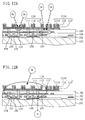
- FIGS. 12A and 12B are views for explaining this problem using the step in FIG. 10A as an example.
- the capacitor 114 When the capacitor 114 is formed on the storage node contact 110, oxygen annealing is required for crystallization of the capacitor insulating film 112 made of a high dielectric film or a ferroelectric film. As shown in FIG. 12A , during this annealing, oxygen gas diffuses from above into the bit line contact 106 and the storage node contact 110, thereby causing poor contact resistance. Further, as shown in FIG. 12B, hydrogen gas occurring in fabrication steps after formation of the capacitor 114 diffuses from above or below the capacitor 114 into the capacitor insulating film 112 made of a high dielectric film or a ferroelectric film, which degrades capacitor properties. As is apparent from the above, the conventional semiconductor memory device suffers contact-resistance rise or interconnect breaks resulting from oxygen diffusion, or capacitor-properties degradation resulting from hydrogen gas, so that it is difficult to attain excellent device properties.
- an object of the present invention is to provide a semiconductor memory device which is designed to have an interlayer insulating film of a relatively great thickness and concurrently to be able to suppress a rise in contact-resistance or the occurrence of interconnect breaks, and to provide a fabrication method of such a device.
- an object of the present invention is to provide a semiconductor memory device which is designed to be able to suppress degradation of capacitor properties resulting from hydrogen gas, and to provide a fabrication method of such a device.
- a semiconductor memory device comprises: a first interlayer insulating film formed on a semiconductor substrate; a capacitor formed above the first interlayer insulating film and composed of a lower electrode, a capacitor insulating film of a high dielectric film or a ferroelectric film, and an upper electrode; a second interlayer insulating film formed over the first interlayer insulating film to cover the capacitor; a first contact plug formed in the first interlayer insulating film to penetrate the first interlayer insulating film; and a second contact plug formed in the second interlayer insulating film to penetrate the second interlayer insulating film to make connection to the first contact plug.
- a first oxygen barrier film is interposed to come into contact with part of the boundary area between the first and second interlayer insulating films.
- the semiconductor memory device With the semiconductor memory device according to one aspect of the present invention, even in the case where the second interlayer insulating film covering the capacitor is thick, the height of the second contact plug is almost the same as the thickness of the second interlayer insulating film. Therefore, in forming the second contact plug, it is sufficient to form the second contact hole with a depth corresponding to the thickness of the second interlayer insulating film, and unlike the conventional example, it is unnecessary to form a contact plug in an opening having a depth corresponding to the total thickness of the first and second interlayer insulating films. This suppresses the occurrence of a void in forming the second contact plug, which prevents the rise in contact resistance or the occurrence of interconnect breaks resulting from poor hole-filling. In particular, if the capacitor is a three-dimensional structure, the second interlayer insulating film covering the capacitor inevitably becomes thick. Even in such a case, the semiconductor memory device according to one aspect of the present invention is more effective.
- the oxygen barrier film is formed between the first and second contact plugs, and the oxygen barrier film is formed to come into contact with at least part of the boundary area between the first and second interlayer insulating films.
- the first oxygen barrier film has the hydrogen barrier property
- the device further comprises a first hydrogen barrier film formed between the first and second interlayer insulating films and between the first interlayer insulating film and the capacitor, and the first oxygen barrier film is formed to penetrate the first hydrogen barrier film.
- the first hydrogen barrier film is made of SiN x that is an insulating material.
- the layers under the capacitor are covered with the first oxygen barrier film and the first hydrogen barrier film having the hydrogen barrier property, which hinders entry of hydrogen from below the capacitor into the capacitor. Therefore, the capacitor insulating film of a high dielectric film or a ferroelectric film can be prevented from being reduced by hydrogen generated in fabrication steps, so that degradation of properties of the capacitor can be avoided. Moreover, by employing the structure in which the entire boundary area between the first and second interlayer insulating films and between the first interlayer insulating film and the capacitor is formed with the first hydrogen barrier film, the layers under the capacitor are fully covered with the hydrogen-barrier material. Therefore, degradation of properties of the capacitor can be completely avoided.
- the semiconductor memory device further comprises a second hydrogen barrier film of insulation formed to cover the capacitor and to come into contact with the first hydrogen barrier film.
- the capacitor insulating film of a high dielectric film or a ferroelectric film can be prevented from being reduced by hydrogen generated in fabrication steps, so that degradation of properties of the capacitor can be completely avoided.
- the first oxygen barrier film has a diameter greater than those of the first and second contact plugs.
- the semiconductor memory device further comprises a third contact plug formed in the first interlayer insulating film to penetrate the first interlayer insulating film, and a second oxygen barrier film is interposed between the third contact plug and the capacitor.
- the second oxygen barrier film has the hydrogen barrier property.
- the area of the device under the capacitor is fully covered with the material having the hydrogen barrier property. Therefore, degradation of properties of the capacitor can be completely avoided.
- At least one of the first and second oxygen barrier films is made of one or more materials selected from the group consisting of Ir, IrO x , TiAIN, TiAl, TiSiN, TaN, TaSiN, TaAlN, and TaAl. More preferably, the first and second oxygen barrier films are made of the same material so that these films are formed simultaneously.
- oxygen can be adequately prevented from entering the contact plugs, and in addition hydrogen can be adequately prevented from diffusing from below into the capacitor insulating film.
- a method for fabricating a semiconductor memory device comprises the steps of: forming a first opening and a second opening in a first interlayer insulating film formed on a semiconductor substrate, the first and second openings penetrating the first interlayer insulating film to reach the semiconductor substrate, respectively; forming a first contact plug in the first opening and a second contact plug in the second opening, the first and second contact plugs making electrical connection to the semiconductor substrate, respectively; forming a first hydrogen barrier film on the first interlayer insulating film, the first contact plug, and the second contact plug; forming a third opening and a fourth opening in the first hydrogen barrier film, the third opening exposing the first contact plug, the fourth opening exposing the second contact plug; forming a first oxygen barrier film in the third opening and a second oxygen barrier film in the fourth opening, the first oxygen barrier film making electrical connection to the first contact plug, the second oxygen barrier film making electrical connection to the second contact plug; forming a capacitor above the second oxygen barrier film, the capacitor being composed of a lower
- the third contact plug With the method for fabricating a semiconductor memory device according to one aspect of the present invention, even in the case where the second interlayer insulating film covering the capacitor is thick, it is sufficient, in forming the third contact plug, to form the third contact hole with a depth corresponding to the thickness of the second interlayer insulating film. Also, unlike the conventional example, it is unnecessary to form a contact plug in an opening having a depth corresponding to the total thickness of the first and second interlayer insulating films. This suppresses the occurrence of a void in forming the third contact plug, which prevents the rise in contact resistance or the occurrence of interconnect breaks resulting from poor hole-filling.
- the oxygen barrier film is formed between the first and third contact plugs.
- first and second oxygen barrier films are formed in the same step, simplification of fabrication steps can be accomplished.
- the first hydrogen barrier film is formed under the capacitor, which hinders entry of hydrogen from below the capacitor into the capacitor. Therefore, the capacitor insulating film of a high dielectric film or a ferroelectric film can be prevented from being reduced by hydrogen generated in fabrication steps, so that degradation of properties of the capacitor can be avoided. Moreover, by employing the first and second oxygen barrier films with the hydrogen barrier property, degradation of properties of the capacitor can be avoided more effectively.
- the third opening has a diameter greater than those of the first opening and the fifth opening.
- the flexibility of the formation position of the third contact plug is enhanced. This suppresses the occurrence of poor connection between the first and third contact plugs.
- the packing density of a semiconductor device advances to a high degree to decrease the diameter of at least one of the first and third contact plugs to an extremely small value, an adequate alignment margin of the fifth opening with respect to the first opening can be provided. Therefore, fabrication of a semiconductor memory device with a high packing density can be facilitated.
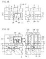
- FIGS. 1A and 1B are views showing the structure of the semiconductor memory device according to the first embodiment of the present invention.
- FIG. 1A is a plan view showing main parts of this structure
- FIG. 1B is a sectional view showing main parts thereof taken along the line Ib - Ib in FIG. 1A.
- a gate electrode 3 is formed in an element formation region defined by an isolation region (STI: shallow trench isolation) 2 in a semiconductor substrate 1 .
- STI shallow trench isolation
- doped layers 4 are formed to interpose the gate electrode 3 .
- the doped layers 4 and the gate electrode 3 constitute a transistor.
- Side-wall insulating films 3a are formed on side surfaces of the gate electrode 3
- a silicide layer 3b is formed on a top surface of the gate electrode 3 .
- a first interlayer insulating film 5 is formed to cover the transistor.
- a first contact plug 6 of tungsten or polysilicon is formed to connect the lower end thereof to the doped layer 4.
- a bit line 7 is formed to connect the lower surface thereof to the upper end of the first contact plug 6.
- a second interlayer insulating film 8 is formed to cover the bit line 7.
- a second contact plug 9 of tungsten or polysilicon is formed to connect the lower end thereof to the doped layer 4.
- a second contact plug 9a is formed to connect the lower end thereof to the top surface of the bit line 7.
- a second contact plug 9b is formed to connect the lower end thereof to the top portion of the gate electrode 3, and concurrently a second contact plug 9c is formed to connect the lower end thereof to the doped layer 4.
- a first hydrogen barrier film 10 of, for example, a silicon nitride film is formed on the second interlayer insulating film 8 and the second contact plugs 9, 9a, 9b, and 9c.
- Third contact plugs 11, 11a, 11b, and 11c are formed through the first hydrogen barrier film 10.
- the lower end of the third contact plug 11 is connected to the upper end of the second contact plug 9, the lower end of the third contact plug 11a is connected to the upper end of the second contact plug 9a, the lower end of the third contact plug 11b is connected to the upper end of the second contact plug 9b, and the lower end of the third contact plug 11c is connected to the upper end of the second contact plug 9c.
- Each of the third contact plugs 11, 11a, 11b, and 11c is made of a TiAIN film or a TiAl film which serves as an oxygen barrier film and also as a hydrogen barrier film.
- As the material for the third contact plugs 11, 11a, 11b, and 11c use can be made of, other than a TiAIN film or a TiAl film, one or more materials selected from the group consisting of an Ir film, an IrO x film, a TiSiN film, a TaN film, a TaSiN film, a TaAlN film, and a TaAl film.
- the first contact plug 6 is a bit line interconnect contact and the second contact plug 9 is a storage node contact.
- the second contact plug 9a provided away from the region formed with a capacitor 18 that will be described later is a bit line contact, and electrically connected to the first contact plug 6.
- the second contact plug 9b is a word line contact and electrically connected to the gate electrode 3 in the region formed with the capacitor 18.
- the second contact plug 9c is a diffusion layer contact.
- the third contact plugs 11a, 11b, and 11c of the same material as the third contact plug 11 are connected to the bit line interconnect contact, the word line contact, and the diffusion layer contact, respectively.
- an oxygen barrier film 12 of a TiAIN film exhibiting conductivity and a first lower electrode 13 of a Pt film are stacked in this order.
- the oxygen barrier film 12 is patterned to connect the lower surface thereof to the upper end of the third contact plug 11.
- the oxygen barrier film 12 is made of a TiAIN film having a thickness of 40 to 150 nm
- the first lower electrode 13 is made of a Pt film having a thickness of 50 to 100 nm.
- a third interlayer insulating film 14 with an opening 14h is formed to cover the oxygen barrier film 12 and the first lower electrode 13. The opening 14h exposes the first lower electrode 13.
- a second lower electrode 15 in a cylindrical shape is formed on an inner wall of the opening 14h, part of the bottom of the opening 14h, and the third interlayer insulating film 14.
- a capacitor insulating film 16 is formed which is made of a high dielectric film or a ferroelectric film (for example, SrBi 2 (Ta 1-x Nb x )O 9 ).
- An upper electrode 17 of a Pt film is formed on the capacitor insulating film 16.
- the capacitor insulating film 16 has a thickness of 50 to 150 nm, and the upper electrode 17 has a thickness of 50 to 100 nm.
- the first and second lower electrodes 13 and 15, the capacitor insulating film 16, and the upper electrode 17 constitute a capacitor 18.
- a fourth interlayer insulating film 19 is formed to cover the capacitor 18.
- the fourth interlayer insulating film 19 is provided for the purpose of electrically isolating adjacent capacitors 18 (not shown).
- a second hydrogen barrier film 20 of an aluminum oxide film (whose thickness is 5 to 100 nm) is formed to come into contact with the side surface of the third interlayer insulating film 14 and the upper and side surfaces of the fourth interlayer insulating film 19. In this structure, the second hydrogen barrier film 20 is in contact with the top surface of the first hydrogen barrier film 10.
- a fifth interlayer insulating film 21 of a SiO 2 film is formed to cover the capacitor 18.
- fourth contact plugs 22a, 22b, and 22c of tungsten or polysilicon are formed through the fifth interlayer insulating film 21 to connect the lower ends thereof to the upper ends of the third contact plugs 11a, 11b, and 11c, respectively.
- interconnect layers 23a, 23b, and 23c are formed to connect the lower surfaces thereof to the upper ends of the fourth contact plugs 22a, 22b, and 22c, respectively.
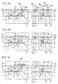
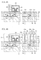
- FIGS. 2A to 2C, FIGS. 3A to 3C, and FIGS. 4A and 4B are sectional views showing main process steps of the method for fabricating a semiconductor memory device according to the first embodiment of the present invention, which are taken along the line Ib - Ib in FIG. 1A.
- the gate electrode 3 is formed in the element formation region defined by the isolation region (STI) 2 in the semiconductor substrate 1. Thereafter, ion implantation using the gate electrode 3 as a mask is performed to form the doped layers 4 in the surface portion of the element formation region. This allows integration of transistors each made of the doped layers 4 and the gate electrode 3. As illustrated in this figure, the side surfaces of the gate electrode 3 are formed with the side-wall insulating films 3a, respectively, and the top surface thereof is formed with the silicide layer 3b.
- STI isolation region
- the first interlayer insulating film 5 of an ozone-based silicon dioxide (SiO 2 ) film having a thickness of 300 to 1000 nm is formed to cover the transistor, and the surface of the formed film is planarized by a CMP method or the like.
- a first contact hole 1h (note that the diameter thereof is 0.22 to 0.24 ⁇ m.) reaching the doped layer 4 is formed through the first interlayer insulating film 5, and then by either a combination of a CVD method and an etch back method or a combination of a CVD method and a CMP method, the first contact hole 1h is filled with tungsten or polysilicon to form the first contact plug 6.
- the bit line 7 of tungsten is formed to connect the lower surface thereof to the upper end of the first contact plug 6.
- the second interlayer insulating film 8 of an ozone-based silicon dioxide (SiO 2 ) film having a thickness of 1000 to 1500 nm is formed to cover the bit line 7, and the surface of the formed film is planarized by a CMP method or the like.
- a second contact hole 2ha reaching the doped layer 4 is formed in the first and second interlayer insulating films 5 and 8
- a second contact hole 2hb reaching the bit line 7 is formed in the second interlayer insulating film 8
- a second contact hole 2hc reaching the gate electrode 3 is formed in the first and second interlayer insulating films 5 and 8
- a second contact hole 2hd reaching the doped layer 4 is formed in the first and second interlayer insulating films 5 and 8 (note that the diameters of the second contact holes 2ha to 2hd are 0.22 to 0.24 ⁇ m).
- the second contact holes 2ha to 2hd are filled with tungsten or polysilicon to form the second contact plugs 9, 9a, 9b and 9c, respectively.
- the first hydrogen barrier film 10 of a silicon nitride (SiN) film is deposited to have a thickness of about 20 to 100 nm.
- the silicon nitride (SiN) film deposition is performed using, for example, a low-pressure CVD method.
- third contact holes 3ha to 3hd (note that the diameters thereof are 0.22 to 0.24 ⁇ m.) exposing the surfaces of the second contact plugs 9, 9a, 9b, and 9c, respectively, are formed in the first hydrogen barrier film 10.
- the third contact holes 3ha to 3hd are filled with a TiAIN film or a TiAl film (the thicknesses thereof are about 100 to 150 nm) to form the third contact plugs 11, 11a, 11b, and 11c (about 100 to 150 nm), respectively.
- the material for the third contact plugs 11, 11a, 11b, and 11c use can be made of, other than a TiAIN film or a TiAl film, one or more materials selected from the group consisting of an Ir film, an IrO x film, a TiSiN film, a TaN film, a TaSiN film, a TaAlN film, and a TaAl film.
- a stacked film made by stacking a TiAIN film and a Pt film in this order from bottom is formed by a sputtering method, and the stacked film is patterned by a dry etching method to form the oxygen barrier film 12 of a TiAIN film and the first lower electrode 13 of a Pt film.
- the oxygen barrier film 12 exhibits not only the oxygen barrier property but also the hydrogen barrier property.
- the third interlayer insulating film 14 of, for example, a silicon dioxide (SiO 2 ) film having a thickness of about 900 to 1000 nm is deposited to cover the oxygen barrier film 12 and the first lower electrode 13, and the surface of the deposited film is planarized using a CMP method or the like.
- the opening 14h exposing the top surface of the first lower electrode 13 is formed through the third interlayer insulating film 14.
- a first platinum film 15a is formed on the third interlayer insulating film 14 including the inside of the opening 14h, and then by etch back, a portion of the first platinum film 15a located on the bottom of the opening 14h is removed to expose the top surface of the first lower electrode 13 from the bottom of the opening 14h.
- a dielectric film 16a of a high dielectric film or a ferroelectric film (for example, SrBi 2 (Ta 1-x Nb x )O 9 with a bismuth-layered perovskite structure) having a thickness of 150 nm is formed on a portion of the first lower electrode 13 exposed in the opening 14h and on the first platinum film 15a.
- a sputtering method a second platinum film 17a is formed on the dielectric film 16a.
- a thermal treatment is performed in an oxygen atmosphere at 650 to 800°C.
- a photoresist pattern is formed on the second platinum film 17a, after which the second platinum film 17a, the dielectric film 16a, and the first platinum film 15a are patterned by a dry etching method to form the second lower electrode 15 of the first platinum film 15a, the capacitor insulating film 16 of the dielectric film 16a, and the upper electrode 17 of the second platinum film 17a.
- the capacitor 18 is provided which is composed of the first lower electrode 13, the second lower electrode 15, the capacitor insulating film 16, and the upper electrode 17. Note that the patterning on the second platinum film 17a, the dielectric film 16a, and the first platinum film 15a is performed by lithography and etching methods with the same mask.
- the fourth interlayer insulating film 19 of an ozone-based silicon dioxide (SiO 2 ) film having a thickness of 500 to 1500 nm is formed to cover a portion of the capacitor 18 located on the third interlayer insulating film 14 and exposed within the opening 14h, and then using a CMP method or the like, the surface of the formed film is planarized to such an extent that the upper electrode 17 is not exposed.
- SiO 2 ozone-based silicon dioxide
- the fourth interlayer insulating film 19 and the third interlayer insulating film 14 are patterned, whereby portions of the fourth and third interlayer insulating films 19 and 14 surrounding the capacitor 18 are allowed to remain and the other portions of the fourth and third interlayer insulating films 19 and 14 are removed to expose the first hydrogen barrier film 10.
- patterning on the fourth and third interlayer insulating films 19 and 14 is performed by lithography and etching methods with the same mask.
- the second hydrogen barrier film 20 of an aluminum oxide film with a thickness of 5 to 100 nm is formed to fully cover the top and side surfaces of the fourth interlayer insulating film 19 and the side surface of the third interlayer insulating film 14.
- the second hydrogen barrier film 20 is in contact with the first hydrogen barrier film 10 of a SiN film.
- the fifth interlayer insulating film 21 of an ozone-based silicon dioxide (SiO 2 ) film having a thickness of 400 to 1000 nm is formed to cover the second hydrogen barrier film 20, and the surface of the formed film is planarized using a CMP method or the like. Subsequently, by a dry etching method, through the fifth interlayer insulating film 21, fourth contact holes 4a to 4c are formed to expose the top surfaces of the third contact plugs 11a to 11c, respectively.
- SiO 2 ozone-based silicon dioxide
- the fourth contact holes 4a to 4c are filled with tungsten or polysilicon to form the fourth contact plugs 22a to 22c, respectively.
- the interconnect 23a whose bottom surface is connected to the upper end of the fourth contact plug 22a, the interconnect 23b whose bottom surface is connected to the upper end of the fourth contact plug 22b, and the interconnect 23c whose bottom surface is connected to the upper end of the fourth contact plug 22c are formed on the fourth interlayer insulating film 21.
- the first hydrogen barrier film 10 is formed to be interposed between the second and third interlayer insulating films 5 and 18, and to be positioned not only in the region on which the capacitor 18 will be formed but also in, for example, the region under which the contact hole reaching the doped layer 4 such as a source region or a drain region is formed.
- the third contact plugs 11a, 11b, and 11c of an oxygen barrier film are formed between the second contact plugs 9a, 9b, and 9c and the fourth contact plugs 22a, 22b, and 22c, respectively, and each of the oxygen barrier films is formed to come into contact with at least part of the boundary area between the second and fifth interlayer insulating films 8 and 21.
- the third contact plugs 11a, 11b, and 11c of an oxygen barrier film have the hydrogen barrier property
- the first hydrogen barrier film 10 is provided in the entire boundary area in interposed relation between the second and fifth interlayer insulating films 8 and 21.
- the layers under the capacitor 18 are fully covered with the third contact plugs 11a, 11b, and 11c and the first hydrogen barrier film 10 that are made of a hydrogen-barrier material, which prevents entry of hydrogen from below the capacitor 18 into the capacitor 18. Therefore, the capacitor insulating film 16 of a high dielectric film or a ferroelectric film can be prevented from being reduced by hydrogen generated in fabrication steps, so that degradation of properties of the capacitor 18 can be avoided.
- the capacitor 18 is completely covered with the first and second hydrogen barrier films 10 and 20. Therefore, the capacitor insulating film 16 made of a high dielectric film or a ferroelectric film can be prevented from being reduced by hydrogen generated in fabrication steps, so that degradation of properties of the capacitor 18 can be avoided.
- the second contact hole 2ha provided in the portion of the first and second interlayer insulating films 5 and 8 located below the capacitor 18 is formed with the second contact plug 9 and the third contact plug 11 of an oxygen barrier film.
- FIG. 5B shows the result of measuring the contact resistances of all measurement points of the devices on the surface of an 8-inch silicon wafer.
- the contact resistances vary over a range of 45 to 7000 ⁇ .
- the reason for this result is as follows: as shown in FIG 5A, during oxygen annealing necessary for crystallization of the capacitor insulating film 16 of a high dielectric film or a ferroelectric film, oxygen 5a entering from above penetrates the third interlayer insulating film 14 to diffuse even into the interfaces of the second contact plugs 9a, 9b, and 9c, whereby the surfaces of the second contact plugs 9a, 9b, and 9c are oxidized.
- the contact resistances of all measurement points on the surface of the silicon wafer fall within a range of 25 to 35 ⁇ . From this result, it is found that the devices with very little variations and lowered resistances are fabricated.
- FIG 6 shows the result of evaluating the remanent polarization (2Pr) of the capacitor 18 before and after hydrogen annealing at 400°C.
- the capacitor 18 in the first embodiment it is found that the remanent polarization properties hardly change before and after the hydrogen annealing.
- This result indicates the following: in the semiconductor memory device according to the first embodiment, all the layers under the capacitor 18 are covered with a hydrogen barrier material, which prevents entry of hydrogen from below the capacitor 18 into the capacitor 18. Moreover, the capacitor 18 is fully covered with the first and second hydrogen barrier films 10 and 20, whereby the capacitor insulating film 16 made of a high dielectric film or a ferroelectric film can be prevented from being reduced by hydrogen generated in fabrication steps, so that degradation of properties of the capacitor 18 can be avoided.
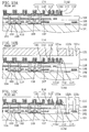
- FIGS. 7A and 7B are views showing the structure of the semiconductor memory device according to the second embodiment of the present invention.
- FIG 7A is a plan view showing main parts of this structure
- FIG. 7B is a sectional view showing main parts thereof taken along the line VIIb - VIIb in FIG. 7A.
- FIGS. 7A and 7B when a comparison is made between the semiconductor memory device according to the second embodiment of the present invention with the above-described semiconductor memory device according to the first embodiment of the present invention, they are different in the design of the third contact plugs 11d, 11e, 11f, and 11g but they are identical in the other components. Hence, the following description will be made mainly of the different point of the design.
- the third contact plug 11e is formed to have a diameter greater than those of the second and fourth contact plugs 9a and 22a
- the third contact plug 11f is formed to have a diameter greater than those of the second and fourth contact plugs 9b and 22b
- the third contact plug 11g is formed to have a diameter greater than those of the second and fourth contact plugs 9c and 22c.
- the second contact plugs 9a, 9b, and 9c and the fourth contact plugs 22a, 22b, and 22c have diameters of 0.22 to 0.24 ⁇ m, while the third contact plugs 11e, 11f, and 11g have diameters equal to or more than 0.08 ⁇ m greater than those of the second contact plugs 9a, 9b, and 9c and the fourth contact plugs 22a, 22b, and 22c.
- the third contact plug 11d is also formed to have a diameter equal to or more than 0.08 ⁇ m greater than that of the second contact plug 9.
- FIGS. 8A and 8B are sectional views showing main process steps of the method for fabricating a semiconductor memory device according to the second embodiment of the present invention, which are taken along the line VIIb - VIIb in FIG. 7A.
- the gate electrode 3 is formed in the element formation region defined by the isolation region (STI) 2 in the semiconductor substrate 1. Thereafter, ion implantation using the gate electrode 3 as a mask is performed to form the doped layers 4 in the surface portion of the element formation region. This allows integration of transistors each made of the doped layers 4 and the gate electrode 3. As illustrated in this figure, the side surfaces of the gate electrode 3 are formed with the side-wall insulating films 3a, respectively, and the top surface thereof is formed with the silicide layer 3b.
- the first interlayer insulating film 5 of an ozone-based silicon dioxide (SiO 2 ) film having a thickness of 300 to 1000 nm is formed to cover the transistor, and the surface of the formed film is planarized by a CMP method or the like.
- a first contact hole 1h (note that the diameter thereof is 0.22 to 0.24 ⁇ m.) reaching the doped layer 4 is formed through the first interlayer insulating film 5, and then by either a combination of a CVD method and an etch back method or a combination of a CVD method and a CMP method, the first contact hole 1h is filled with tungsten or polysilicon to form the first contact plug 6.
- the bit line 7 of tungsten is formed to connect the lower surface thereof to the upper end of the first contact plug 6.
- the second interlayer insulating film 8 of an ozone-based silicon dioxide (SiO 2 ) film having a thickness of 1000 to 1500 nm is formed to cover the bit line 7, and the surface of the formed film is planarized by a CMP method or the like.
- the second contact hole 2ha reaching the doped layer 4 is formed in the first and second interlayer insulating films 5 and 8
- the second contact hole 2hb reaching the bit line 7 is formed in the second interlayer insulating film 8
- the second contact hole 2hc reaching the gate electrode 3 is formed in the first and second interlayer insulating films 5 and 8
- the second contact hole 2hd reaching the doped layer 4 is formed in the first and second interlayer insulating films 5 and 8 (note that the diameters of the second contact holes 2ha to 2hd are 0.22 to 0.24 ⁇ m).
- the second contact holes 2ha to 2hd are filled with tungsten or polysilicon to form the second contact plugs 9, 9a, 9b and 9c.
- the first hydrogen barrier film 10 of a silicon nitride film (a SiN film) is deposited to have a thickness of about 20 to 100 nm. In this step, it is recommended that the silicon nitride film (the SiN film) deposition is performed using, for example, a low-pressure CVD method.
- third contact holes 3hp to 3hs (note that the diameters thereof are 0.22 to 0.24 ⁇ m.) exposing the surfaces of the second contact plugs 9, 9a, 9b, and 9c, respectively, are formed in the first hydrogen barrier film 10. Thereafter, by either a combination of a CVD method and an etch back method or a combination of a CVD method and a CMP method, the third contact holes 3hp to 3hs are filled with a TiAIN film or a TiAl film (the thicknesses thereof are about 100 to 150 nm) to form the third contact plugs 11d, 11e, 11f, and 11g, respectively (the thicknesses thereof are about 100 to 150 nm).
- the semiconductor memory device and its fabrication method according to the second embodiment of the present invention can exert not only the above-mentioned effects of the semiconductor memory device and its fabrication method according to the first embodiment of the present invention but also the following effects.
- the third contact plugs 11e, 11f, and 11g serving as oxygen barrier films have diameters greater than those of the second contact plugs 9a, 9b, and 9c and the fourth contact plugs 22a, 22b, and 22c. Therefore, when the fourth contact plugs 22a, 22b, and 22c are formed to make electrical connection to the second contact plugs 9a, 9b, and 9c, respectively, the flexibility of the formation position of the fourth contact plugs 22a, 22b, and 22c is enhanced.
- an alignment margin in lithography of 0.04 ⁇ m can be secured between the second contact holes 2hb, 2hc, and 2hd and the fourth contact holes 4a, 4b, and 4c, respectively.
- SrBi 2 (Ta 1-x Nb x )O 9 has been given as an exemplary material forming the capacitor insulating film 16.
- lead zirconate titanate, barium strontium titanate, tantalum pentoxide, or the like can provide the same effects as those described above.
- the contact hole formed can have a reduced aspect ratio. Moreover, since the oxygen barrier film is buried in the contact hole, oxidation of the contact plug by sintering of the high dielectric film or the ferroelectric film in an oxygen atmosphere can be prevented. Therefore, a highly reliable semiconductor memory device capable of stable operations can be attained.
- the semiconductor memory device and its fabrication method according to the present invention is useful in a semiconductor memory device or the like which is provided with a capacitor element of a three-dimensional structure having a capacitor insulating film of a ferroelectric film or a high dielectric film, and also useful in a fabrication method of such a device.
Landscapes
- Engineering & Computer Science (AREA)
- Manufacturing & Machinery (AREA)
- Semiconductor Memories (AREA)
Applications Claiming Priority (1)
| Application Number | Priority Date | Filing Date | Title |
|---|---|---|---|
| JP2005156740A JP4766924B2 (ja) | 2005-05-30 | 2005-05-30 | 半導体記憶装置及びその製造方法 |
Publications (2)
| Publication Number | Publication Date |
|---|---|
| EP1729329A2 true EP1729329A2 (fr) | 2006-12-06 |
| EP1729329A3 EP1729329A3 (fr) | 2008-12-31 |
Family
ID=37025062
Family Applications (1)
| Application Number | Title | Priority Date | Filing Date |
|---|---|---|---|
| EP06008232A Withdrawn EP1729329A3 (fr) | 2005-05-30 | 2006-04-20 | Cellule de mémoire semiconductrice avec condensateur ferroélectrique et son procédé de fabrication |
Country Status (4)
| Country | Link |
|---|---|
| US (1) | US7456455B2 (fr) |
| EP (1) | EP1729329A3 (fr) |
| JP (1) | JP4766924B2 (fr) |
| KR (1) | KR20060124560A (fr) |
Families Citing this family (5)
| Publication number | Priority date | Publication date | Assignee | Title |
|---|---|---|---|---|
| JP4308691B2 (ja) * | 2004-03-19 | 2009-08-05 | 富士通マイクロエレクトロニクス株式会社 | 半導体基板および半導体基板の製造方法 |
| JP2009253033A (ja) * | 2008-04-07 | 2009-10-29 | Panasonic Corp | 半導体記憶装置及びその製造方法 |
| WO2010032456A1 (fr) * | 2008-09-16 | 2010-03-25 | ローム株式会社 | Dispositif de stockage à semi-conducteur et son procede de fabrication |
| KR20130001513A (ko) * | 2011-06-27 | 2013-01-04 | 삼성디스플레이 주식회사 | 표시장치 및 그 제조방법 |
| US20150206893A1 (en) * | 2014-01-20 | 2015-07-23 | Cypress Semiconductor Corporation | Damascene oxygen barrier and hydrogen barrier for ferroelectric random-access memory |
Citations (2)
| Publication number | Priority date | Publication date | Assignee | Title |
|---|---|---|---|---|
| JPH10242418A (ja) | 1997-02-25 | 1998-09-11 | Sony Corp | Dramおよびその製造方法 |
| JP2005156740A (ja) | 2003-11-21 | 2005-06-16 | Canon Inc | 符号化装置、復号化装置、符号化方法、復号化方法及びプログラム |
Family Cites Families (14)
| Publication number | Priority date | Publication date | Assignee | Title |
|---|---|---|---|---|
| JP3569112B2 (ja) * | 1997-07-17 | 2004-09-22 | 株式会社東芝 | 半導体集積回路およびその製造方法 |
| JPH11126881A (ja) * | 1997-10-23 | 1999-05-11 | Hitachi Ltd | 高強誘電体薄膜コンデンサを有する半導体装置及びその製造方法 |
| JP2002141482A (ja) * | 2000-11-07 | 2002-05-17 | Sanyo Electric Co Ltd | 半導体装置およびその製造方法 |
| US7075134B2 (en) * | 2001-11-29 | 2006-07-11 | Symetrix Corporation | Ferroelectric and high dielectric constant integrated circuit capacitors with three-dimensional orientation for high-density memories, and method of making the same |
| US6656748B2 (en) * | 2002-01-31 | 2003-12-02 | Texas Instruments Incorporated | FeRAM capacitor post stack etch clean/repair |
| JP2003289134A (ja) * | 2002-03-28 | 2003-10-10 | Matsushita Electric Ind Co Ltd | 半導体装置及びその製造方法 |
| US7186569B2 (en) * | 2002-08-02 | 2007-03-06 | Unity Semiconductor Corporation | Conductive memory stack with sidewall |
| JP3621087B1 (ja) * | 2002-11-13 | 2005-02-16 | 松下電器産業株式会社 | 半導体装置及びその製造方法 |
| JP2004228422A (ja) * | 2003-01-24 | 2004-08-12 | Renesas Technology Corp | 半導体装置及びその製造方法 |
| JP3964798B2 (ja) * | 2003-01-31 | 2007-08-22 | 松下電器産業株式会社 | 誘電体メモリ及びその製造方法 |
| JP2004296534A (ja) * | 2003-03-25 | 2004-10-21 | Seiko Epson Corp | 半導体装置、半導体装置の製造方法、強誘電体メモリ、及び電子機器 |
| JP3920863B2 (ja) * | 2003-03-25 | 2007-05-30 | 三洋電機株式会社 | メモリの製造方法 |
| JP4025232B2 (ja) * | 2003-04-07 | 2007-12-19 | 株式会社東芝 | 半導体記憶装置及びその製造方法 |
| JP2005229001A (ja) * | 2004-02-16 | 2005-08-25 | Toshiba Corp | 半導体装置及び半導体装置の製造方法 |
-
2005
- 2005-05-30 JP JP2005156740A patent/JP4766924B2/ja not_active Expired - Fee Related
-
2006
- 2006-04-20 EP EP06008232A patent/EP1729329A3/fr not_active Withdrawn
- 2006-04-25 KR KR1020060037096A patent/KR20060124560A/ko not_active Withdrawn
- 2006-05-19 US US11/436,648 patent/US7456455B2/en not_active Expired - Fee Related
Patent Citations (2)
| Publication number | Priority date | Publication date | Assignee | Title |
|---|---|---|---|---|
| JPH10242418A (ja) | 1997-02-25 | 1998-09-11 | Sony Corp | Dramおよびその製造方法 |
| JP2005156740A (ja) | 2003-11-21 | 2005-06-16 | Canon Inc | 符号化装置、復号化装置、符号化方法、復号化方法及びプログラム |
Also Published As
| Publication number | Publication date |
|---|---|
| EP1729329A3 (fr) | 2008-12-31 |
| US7456455B2 (en) | 2008-11-25 |
| KR20060124560A (ko) | 2006-12-05 |
| JP2006332488A (ja) | 2006-12-07 |
| US20060267060A1 (en) | 2006-11-30 |
| JP4766924B2 (ja) | 2011-09-07 |
Similar Documents
| Publication | Publication Date | Title |
|---|---|---|
| US7002199B2 (en) | Semiconductor device using high-dielectric-constant material and method of manufacturing the same | |
| US6750492B2 (en) | Semiconductor memory with hydrogen barrier | |
| KR100449949B1 (ko) | 강유전체 메모리 소자의 캐패시터 제조방법 | |
| US6762445B2 (en) | DRAM memory cell with dummy lower electrode for connection between upper electrode and upper layer interconnect | |
| US6916705B2 (en) | Semiconductor memory and method for fabricating the same | |
| US20090001437A1 (en) | Integrated Circuit Devices Including Recessed Conductive Layers and Related Methods | |
| US6261849B1 (en) | Method of forming integrated circuit capacitors having recessed oxidation barrier spacers and method of forming same | |
| US6888189B2 (en) | Dielectric element including oxide-based dielectric film and method of fabricating the same | |
| US6784474B2 (en) | Semiconductor memory device and method for fabricating the same | |
| US6030866A (en) | Method of manufacturing a capacitor | |
| US7732851B2 (en) | Method for fabricating a three-dimensional capacitor | |
| US6844581B2 (en) | Storage capacitor and associated contact-making structure and a method for fabricating the storage capacitor and the contact-making structure | |
| JP2003086771A (ja) | 容量素子、半導体記憶装置及びその製造方法 | |
| US20040164323A1 (en) | Ferroelectric memory devices with enhanced ferroelectric properties and methods for fabricating such memory devices | |
| US7456455B2 (en) | Semiconductor memory device and method for fabricating the same | |
| KR100843143B1 (ko) | 반도체 소자 및 이의 제조 방법 | |
| US6534810B2 (en) | Semiconductor memory device having capacitor structure formed in proximity to corresponding transistor | |
| US6964899B2 (en) | Semiconductor device and method of manufacturing the same | |
| JP2002190580A (ja) | 半導体装置およびその製造方法 | |
| US6853026B2 (en) | Semiconductor device | |
| KR100531462B1 (ko) | 엠티피 구조의 캐패시터를 구비하는 강유전체 메모리소자의 제조 방법 | |
| JP2004235560A (ja) | 誘電体メモリ及びその製造方法 | |
| JP2004179497A (ja) | 半導体装置および半導体装置の製造方法 | |
| KR101109888B1 (ko) | 반도체장치 및 그 제조방법 | |
| JP2009158704A (ja) | 半導体装置及びその製造方法 |
Legal Events
| Date | Code | Title | Description |
|---|---|---|---|
| PUAI | Public reference made under article 153(3) epc to a published international application that has entered the european phase |
Free format text: ORIGINAL CODE: 0009012 |
|
| AK | Designated contracting states |
Kind code of ref document: A2 Designated state(s): AT BE BG CH CY CZ DE DK EE ES FI FR GB GR HU IE IS IT LI LT LU LV MC NL PL PT RO SE SI SK TR |
|
| AX | Request for extension of the european patent |
Extension state: AL BA HR MK YU |
|
| 17P | Request for examination filed |
Effective date: 20070124 |
|
| RAP1 | Party data changed (applicant data changed or rights of an application transferred) |
Owner name: PANASONIC CORPORATION |
|
| PUAL | Search report despatched |
Free format text: ORIGINAL CODE: 0009013 |
|
| AK | Designated contracting states |
Kind code of ref document: A3 Designated state(s): AT BE BG CH CY CZ DE DK EE ES FI FR GB GR HU IE IS IT LI LT LU LV MC NL PL PT RO SE SI SK TR |
|
| AX | Request for extension of the european patent |
Extension state: AL BA HR MK YU |
|
| RIC1 | Information provided on ipc code assigned before grant |
Ipc: H01L 27/108 20060101ALN20081125BHEP Ipc: H01L 27/105 20060101ALI20081125BHEP Ipc: H01L 21/8247 20060101ALI20081125BHEP Ipc: H01L 21/8242 20060101ALI20081125BHEP Ipc: H01L 21/768 20060101ALI20081125BHEP Ipc: H01L 21/02 20060101AFI20061009BHEP |
|
| AKX | Designation fees paid |
Designated state(s): DE FR GB |
|
| STAA | Information on the status of an ep patent application or granted ep patent |
Free format text: STATUS: THE APPLICATION IS DEEMED TO BE WITHDRAWN |
|
| 18D | Application deemed to be withdrawn |
Effective date: 20090701 |