EP1729348A2 - Boîte de jonction pour un module de cellule solaire - Google Patents
Boîte de jonction pour un module de cellule solaire Download PDFInfo
- Publication number
- EP1729348A2 EP1729348A2 EP06010045A EP06010045A EP1729348A2 EP 1729348 A2 EP1729348 A2 EP 1729348A2 EP 06010045 A EP06010045 A EP 06010045A EP 06010045 A EP06010045 A EP 06010045A EP 1729348 A2 EP1729348 A2 EP 1729348A2
- Authority
- EP
- European Patent Office
- Prior art keywords
- clamping
- connection
- conductor
- clamping device
- solar cell
- Prior art date
- Legal status (The legal status is an assumption and is not a legal conclusion. Google has not performed a legal analysis and makes no representation as to the accuracy of the status listed.)
- Granted
Links
Images

Classifications
-
- H—ELECTRICITY
- H02—GENERATION; CONVERSION OR DISTRIBUTION OF ELECTRIC POWER
- H02S—GENERATION OF ELECTRIC POWER BY CONVERSION OF INFRARED RADIATION, VISIBLE LIGHT OR ULTRAVIOLET LIGHT, e.g. USING PHOTOVOLTAIC [PV] MODULES
- H02S40/00—Components or accessories in combination with PV modules, not provided for in groups H02S10/00 - H02S30/00
- H02S40/30—Electrical components
- H02S40/34—Electrical components comprising specially adapted electrical connection means to be structurally associated with the PV module, e.g. junction boxes
-
- H—ELECTRICITY
- H01—ELECTRIC ELEMENTS
- H01R—ELECTRICALLY-CONDUCTIVE CONNECTIONS; STRUCTURAL ASSOCIATIONS OF A PLURALITY OF MUTUALLY-INSULATED ELECTRICAL CONNECTING ELEMENTS; COUPLING DEVICES; CURRENT COLLECTORS
- H01R4/00—Electrically-conductive connections between two or more conductive members in direct contact, i.e. touching one another; Means for effecting or maintaining such contact; Electrically-conductive connections having two or more spaced connecting locations for conductors and using contact members penetrating insulation
- H01R4/28—Clamped connections, spring connections
- H01R4/48—Clamped connections, spring connections utilising a spring, clip, or other resilient member
- H01R4/4809—Clamped connections, spring connections utilising a spring, clip, or other resilient member using a leaf spring to bias the conductor toward the busbar
- H01R4/48185—Clamped connections, spring connections utilising a spring, clip, or other resilient member using a leaf spring to bias the conductor toward the busbar adapted for axial insertion of a wire end
- H01R4/4819—Clamped connections, spring connections utilising a spring, clip, or other resilient member using a leaf spring to bias the conductor toward the busbar adapted for axial insertion of a wire end the spring shape allowing insertion of the conductor end when the spring is unbiased
- H01R4/4821—Single-blade spring
-
- H—ELECTRICITY
- H01—ELECTRIC ELEMENTS
- H01R—ELECTRICALLY-CONDUCTIVE CONNECTIONS; STRUCTURAL ASSOCIATIONS OF A PLURALITY OF MUTUALLY-INSULATED ELECTRICAL CONNECTING ELEMENTS; COUPLING DEVICES; CURRENT COLLECTORS
- H01R13/00—Details of coupling devices of the kinds covered by groups H01R12/70 or H01R24/00 - H01R33/00
- H01R13/02—Contact members
- H01R13/10—Sockets for co-operation with pins or blades
- H01R13/11—Resilient sockets
- H01R13/113—Resilient sockets co-operating with pins or blades having a rectangular transverse section
-
- H—ELECTRICITY
- H01—ELECTRIC ELEMENTS
- H01R—ELECTRICALLY-CONDUCTIVE CONNECTIONS; STRUCTURAL ASSOCIATIONS OF A PLURALITY OF MUTUALLY-INSULATED ELECTRICAL CONNECTING ELEMENTS; COUPLING DEVICES; CURRENT COLLECTORS
- H01R4/00—Electrically-conductive connections between two or more conductive members in direct contact, i.e. touching one another; Means for effecting or maintaining such contact; Electrically-conductive connections having two or more spaced connecting locations for conductors and using contact members penetrating insulation
- H01R4/28—Clamped connections, spring connections
- H01R4/48—Clamped connections, spring connections utilising a spring, clip, or other resilient member
- H01R4/4809—Clamped connections, spring connections utilising a spring, clip, or other resilient member using a leaf spring to bias the conductor toward the busbar
- H01R4/4811—Spring details
- H01R4/4816—Spring details the spring shape preventing insertion of the conductor end when the spring is unbiased
-
- H—ELECTRICITY
- H01—ELECTRIC ELEMENTS
- H01R—ELECTRICALLY-CONDUCTIVE CONNECTIONS; STRUCTURAL ASSOCIATIONS OF A PLURALITY OF MUTUALLY-INSULATED ELECTRICAL CONNECTING ELEMENTS; COUPLING DEVICES; CURRENT COLLECTORS
- H01R4/00—Electrically-conductive connections between two or more conductive members in direct contact, i.e. touching one another; Means for effecting or maintaining such contact; Electrically-conductive connections having two or more spaced connecting locations for conductors and using contact members penetrating insulation
- H01R4/28—Clamped connections, spring connections
- H01R4/48—Clamped connections, spring connections utilising a spring, clip, or other resilient member
- H01R4/4809—Clamped connections, spring connections utilising a spring, clip, or other resilient member using a leaf spring to bias the conductor toward the busbar
- H01R4/4846—Busbar details
- H01R4/485—Single busbar common to multiple springs
-
- Y—GENERAL TAGGING OF NEW TECHNOLOGICAL DEVELOPMENTS; GENERAL TAGGING OF CROSS-SECTIONAL TECHNOLOGIES SPANNING OVER SEVERAL SECTIONS OF THE IPC; TECHNICAL SUBJECTS COVERED BY FORMER USPC CROSS-REFERENCE ART COLLECTIONS [XRACs] AND DIGESTS
- Y02—TECHNOLOGIES OR APPLICATIONS FOR MITIGATION OR ADAPTATION AGAINST CLIMATE CHANGE
- Y02E—REDUCTION OF GREENHOUSE GAS [GHG] EMISSIONS, RELATED TO ENERGY GENERATION, TRANSMISSION OR DISTRIBUTION
- Y02E10/00—Energy generation through renewable energy sources
- Y02E10/50—Photovoltaic [PV] energy
Definitions
- the invention relates to an electrical connection and junction box for a solar cell module connected to thinnatiorbändem solar cells, with a housing and provided in the housing electrical and / or electronic devices and at least one provided in the housing and at least one clamping device having electrical connection device.
- a voltage applied to the shaded solar cell depends on the position of the shaded solar cell in the series connection. If this voltage applied to the shaded solar cell is greater than its blocking voltage, a breakdown and thus permanent damage to the solar cell will occur in the solar cell. Even if there should be no damage to the solar cell by a breakdown, a large power loss is implemented in the shaded solar cell, so that heats up the shaded solar cell. Such heating can also lead to damage to the shaded solar cell and to the solar cells adjacent to it.
- bypass diodes are often used, which are connected in anti-parallel to the solar cells. In this way, it is achieved that a shaded solar cell does not contribute more to the total voltage of the solar cell module, but the current flow is still maintained. The solar cell module thus only shows a reduced operating voltage, but does not completely fail. In addition, no power is converted in the shaded solar cell, so that damage to the shaded solar cell can be avoided.
- each solar cell of a solar cell module could be associated with exactly one diode. Frequently, however, the procedure is such that a plurality of solar cells connected in series is respectively protected by a common diode.
- Electrical connection and connection boxes which are used for solar cell modules, thus generally always have a plurality of bypass diodes in addition, in the electrical connection and connection boxes further electrical and / or electronic devices may be provided, so that the electrical connection and Junction fed conductor must be connected to the electrical and / or electronic devices, such as the bypass diodes.
- the solar cells in a solar cell module are generally connected to one another with thin conductor strips, so-called strings. These conductor strips typically have a thickness of a few tenths of a millimeter (about 0.3 mm) and a width of a few millimeters (about 3-8 mm). These individual solar cells of the solar cell module interconnecting conductor strips are guided out of the solar cell module, so that the thin conductor strips can be used directly for connection purposes.
- the bypass diodes are usually arranged on a printed circuit board, which is connected to a connection device of the connection and junction box.
- the connecting device is connected via at least one conductor strip to the solar cell module.
- the conductor strips are typically inserted into the electrical connection and junction box from below, which has a removable cover, so that the individual conductor strips can be contacted by hand with the provided in the housing of the connection and junction box electrical connection device.
- These are the solar cell module, relative to the housing of the connection and junction box from below coming thin conductor strips generally bent by 180 °, to then be connected from above, for example, via a clamping device to the terminal device.
- Such a bending is readily possible, since the thin conductor strips, which are typically made of metal, are very flexible due to their dimensions, in particular their small thickness. However, this procedure is very complicated and time-consuming, and connection errors can not be avoided without further ado.
- connection and connection boxes of disadvantage that due to the limited outer dimensions of the housing usually inside the connection and junction box, the electrical and / or electronic devices and the connection device must be arranged very close to each other. As a result, only a very small space is available for the connection of the conductor strips, which complicates the connection.
- the previously derived and indicated object is achieved in a first alternative embodiment of the invention in that the clamping device for producing a clamping contact between the terminal device and a conductor strip is designed and arranged such that at least one of led out of the solar cell module thin conductor strip in two different opposite insertion directions in the clamping device is inserted.
- the invention goes a completely new way by leading out of the solar cell module and serving to connect the solar cells thin conductor strips according to the invention in two different preferably opposite insertion directions in the clamping device inserted and thus connectable to the electrical connection device.
- the invention it is possible, on the one hand, to introduce the thin conductor strips serving to connect the solar cells from below and, on the other hand, from above, into the clamping device.
- the invention thus avoids the costly, known from the prior art approach to lead the thin conductor strips for connecting the solar cells in the connection and junction box only upwards and then bend by up to 180 ° to supply them to the terminal device.
- the required effort is thus considerably reduced by the invention.
- connection device in a connection and connection box according to the invention for a solar cell module.
- connection and junction box according to the invention, moreover, the connection of lead out of the solar cell module thin conductor strips is further simplified, since the connection and junction box of the invention can be placed from two terminal sides on the solar cell module to the conductor strips from below into the electrical connection device introduce.
- the clamping device is designed and arranged such that both a terminal contact with at least one conductor strip and a terminal contact with at least one preferably circular terminal conductor of an electronic component, in particular a connecting conductor of a bypass diode, by introducing the conductor strip or, the connecting conductor in the clamping device can be produced.
- the invention is based on the basic idea of forming a clamping device both for the connection of the conductor strip and for the connection of an electronic component, such as a bypass diode.
- connection and connection box may preferably be arranged side by side.
- first lead of an electronic component preferably a bypass diode
- bypass diodes it is no longer necessary to arrange, for example, the bypass diodes on a printed circuit board, as is usually provided in the connection and junction boxes known from the prior art. This helps to increase the free space available inside the can for connecting the conductor strips, which facilitates connection.
- connection and junction box according to the invention clamping devices can be connected as needed with a conductor strip and / or with a terminal conductor of an electronic component, resulting in a simple construction of the junction box according to the invention and a high flexibility at the arrangement of the connection device in the connection and connection box according to the invention leads.
- the clamping device is formed ⁇ -shaped with two connected via a arranged in the bottom region of the clamping device bottom portion clamping legs which converge towards a clamping portion of the clamping device and the end pass into diverging insertion bevels, so that the clamping device in the clamping section has a substantially X-shaped cross-section.
- the ⁇ -shaped design of the clamping device contributes to the fact that it is possible in a simple manner to introduce a conductor strip and / or a terminal conductor of an electronic component from above via the insertion bevels in the clamping portion.
- ⁇ -shaped clamping devices can be produced in a simple manner and enable reliable electrical contacting of the conductors introduced into the clamping section.
- the bottom portion has a recess which may be formed for insertion of a conductor strip.
- the bottom-side insertion section extends in the longitudinal direction of the clamping portion, starting from the longitudinal sides of the clamping legs in the direction of the central region of the clamping legs.
- the bottom-side insertion section is formed as a slot-shaped recess of the bottom portion. If necessary, it can also be provided that the bottom portion has a plurality of longitudinally adjacent insertion portions, which allow the insertion of a conductor strip in the clamping device through the bottom portion therethrough.
- the Clamping leg of a clamping device in the clamping portion has at least one outwardly curved preferably cup-shaped further insertion section for the lead and that, more preferably, the further insertion of a clamping leg and the further insertion of the other clamping leg are arranged opposite one another.
- the two opposite insertion sections complement each other to form a substantially nut-shaped opening of the clamping portion. If a circular lead is introduced into this insertion, a secure electrical contact is ensured by the larger contact surface between the lead and the clamping leg.
- the connection device may comprise a current bar, to which preferably two clamping devices can be clamped in such a way that via the current bar a line contact between at least one conductor strip introduced into the first clamping device and at least one connecting conductor introduced into the second clamping device, preferably a connecting conductor of a bypass diode, can be produced.
- a line contact between at least one conductor strip introduced into the first clamping device and at least one connecting conductor introduced into the second clamping device, preferably a connecting conductor of a bypass diode can be produced.
- After clamping the clamping device on the current bar of the current bar runs between the clamping portion and is clamped between two clamping legs.
- That conductor strip and / or the connecting conductor must be inserted into the clamping region formed between the current bar and one of the clamping legs. The conductor strip or the connecting conductor are thus clamped between the current bar and a clamping leg of the clamping device.
- the current bar may be web-shaped with preferably substantially mutually perpendicular web end sections.
- a clamping device is provided in each case on both web end sections, moreover preferably in a connected state, a conductor strip is connected to the one clamping device and a connecting conductor to the other clamping device.
- the current bar is formed substantially U-shaped and has a straight and an angled conductor legs.
- a terminal may be provided for connection of the terminal device to a line contact, which leads out of the connection and junction box.
- the terminal may be a tension spring clamp. In principle, however, other forms of terminals can be used.
- the current bar ensures a particularly simple installation of the connection device in the housing of the connection and junction box and a comparatively large space available for connecting the conductor strips available space, it is of course also provided, the current bar depending on the structural design the connection and junction box or the arrangement of provided in the housing electrical and / or electronic devices, if necessary, to adapt to the actual space conditions.
- the clamping legs and / or the bottom portion may be made of a spring material. This facilitates the production and leads to low production costs. In principle, however, it is also possible that the clamping legs are spring-loaded in order to provide a sufficient clamping force in the region of the clamping section.
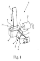
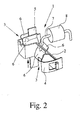
- a connecting device 1 which can be used to connect a not shown in detail according to the invention junction and junction box to a solar cell module.
- the connecting device 1 has a current bar 2 and two clamping devices 3, which are clamped on the current bar 2. In principle, more than two clamping devices 3 can be clamped on the current bar 2.
- the current bar 2 at a free end to a terminal 4, in the present case a tension spring clamp.
- the connection device 1 is arranged within the electrical connection and junction box and connected to the solar cell module via thin conductor strips 5.
- the clamping device 3 is designed and arranged for the production of a clamping contact such that at least one led out of the solar cell module thin conductor strip 5 in at least two different opposite insertion directions in the clamping device 3 can be inserted.
- FIGS. 1 and 2 wherein, according to FIG. 1, the conductor strip 5 is inserted from above into the clamping device 3 and according to FIG. 2 from below into the clamping device 3. After insertion of the conductor strip 5 in the clamping device 3, the conductor strip 5 is clamped between a clamping leg 6 of the clamping device 3 and the current bar 2.
- the clamping device 3 is designed and arranged such that both a clamping contact with at least one conductor strip 5 and a clamping contact with at least one preferably circular terminal conductor 7 of an electronic component by inserting of the conductor strip 5 and the lead 7 in the clamping device 3 can be produced.
- a circular connecting conductor 7 of a bypass diode 8 is inserted into a further clamping device 3, which is clamped to the current bar 2.
- the further clamping device 3 is clamped in the embodiments shown in FIGS. 1 and 2 at a free end of an angled conductor limb of the presently U-shaped current bar 2.
- the current bar 2 is web-shaped.
- the connecting device 1 only has a clamping device 3 for connection to a conductor strip 5 and a bypass diode 8, it is preferably provided for each conductor strip 5 and 8 for each diode 8 each provide a clamping device. This facilitates the connection of the conductor strip 5 to the terminal device.
- the clamping device 3 When inserting the connecting conductor 7 of the bypass diode 8 in the clamping device 3, the connecting conductor 7 is guided or clamped between a clamping leg 6 of the clamping device 3 and the current bar 2.
- the clamping device 3 has two cooperating clamping legs 6, wherein each clamping leg 6 has at least one outwardly curved, preferably cup-shaped, further insertion section 9 for the connecting conductor 7 in the clamping section and wherein according to FIG Embodiment of the further insertion section 9 of a clamping leg 6 and the further insertion section 9 of the other clamping leg 6 may be arranged opposite one another can.
- the cup-shaped bulge of the further insertion section 9 ensures that there is a secure clamping contact between the connecting conductor 7 and the current bar 2 after insertion of the connecting conductor 7 in the insertion section 9.
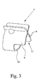
- FIGS. 1 and 2 one of the clamping devices 3 provided in FIGS. 1 and 2 for connection to the conductor strip 5 or to the connecting conductor 7 is shown in a schematic view from the side.
- the clamping device 3 is formed ⁇ -shaped and has two connected via a arranged in the bottom region of the clamping device 3 bottom portion 10 clamping legs 6, which converge toward one another in the direction of a clamping portion of the clamping device 3 and merge into diverging insertion bevels end, so that the clamping device 3 in Clamping portion has a substantially X-shaped cross-section.
- the clamping legs 6 are only partially connected via the bottom portion 10 with each other.
- a bottom-side insertion section 11 extends over which it is possible to introduce a conductor strip 5 from below in the direction of the clamping gap in the clamping device 3.
- the clamping legs 6 and / or the bottom portion 10 are made of a spring material to apply the clamping force necessary for clamping the clamping device 3 on the current bar 2 and the clamping of the conductor strip 5 and / or the connecting conductor 7.
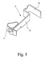
- FIG. 5 shows the current bar 2 of the connection device 1 shown in FIGS. 1 and 2.
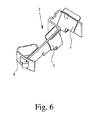
- the current bar 2 is essentially U-shaped and has a straight conductor leg 12 and an angled conductor leg 13.
- the current bar 2 is bar-shaped formed, wherein at a free end of the angled conductor leg 13, the terminal 4 is provided.
- Fig. 6 the current bar 2 shown in Fig. 5 is shown again, wherein two clamping devices 3 are clamped on the current bar 2.
- the invention goes a completely new way by the flexible thin conductor strips 5 inserted both from above and from below into the housing of the electrical connection and junction box can be connected starting from two sides with the connecting device 1.
- a space-saving installation of the connection device 1 in the can is made possible by the provided in the connection and junction box according to the invention training the connection device 1.
- the bypass diodes 8 can be connected in a simple manner with the current bar 2 via a clamping device 3, wherein for connecting the conductor strips 5 and for connecting the connecting conductor 7 structurally identically designed clamping devices 3 can be used. Both contribute to the fact that a simple and secure connection out of the solar cell module led out thin conductor strips 5 is made possible.
Landscapes
- Photovoltaic Devices (AREA)
Applications Claiming Priority (1)
| Application Number | Priority Date | Filing Date | Title |
|---|---|---|---|
| DE102005025976A DE102005025976B4 (de) | 2005-06-03 | 2005-06-03 | Elektrische Anschluß- und Verbindungsdose für ein Solarzellenmodul |
Publications (3)
| Publication Number | Publication Date |
|---|---|
| EP1729348A2 true EP1729348A2 (fr) | 2006-12-06 |
| EP1729348A3 EP1729348A3 (fr) | 2008-12-31 |
| EP1729348B1 EP1729348B1 (fr) | 2010-10-06 |
Family
ID=36997258
Family Applications (1)
| Application Number | Title | Priority Date | Filing Date |
|---|---|---|---|
| EP06010045A Expired - Lifetime EP1729348B1 (fr) | 2005-06-03 | 2006-05-16 | Boîte de jonction pour un module de cellule solaire |
Country Status (5)
| Country | Link |
|---|---|
| US (1) | US7530837B2 (fr) |
| EP (1) | EP1729348B1 (fr) |
| AT (1) | ATE484077T1 (fr) |
| DE (2) | DE102005025976B4 (fr) |
| ES (1) | ES2351799T3 (fr) |
Cited By (9)
| Publication number | Priority date | Publication date | Assignee | Title |
|---|---|---|---|---|
| EP1976026A2 (fr) * | 2007-03-28 | 2008-10-01 | Günther Spelsberg GmbH & Co. KG | Boîtier de jonction |
| WO2009086874A1 (fr) | 2008-01-08 | 2009-07-16 | Yamaichi Electronics Deutschland Gmbh | Boîte de jonction, utilisation, panneau solaire, élément de contact et procédé |
| WO2009150104A3 (fr) * | 2008-06-12 | 2010-10-07 | Anton Gensler Gmbh | Boîte de jonction pour modules photovoltaïques |
| WO2010054837A3 (fr) * | 2008-11-14 | 2011-04-21 | Yamaichi Electronics Deutschland Gmbh | Panneau solaire, procédé de fabrication de ce panneau solaire et boîtier de pontage |
| WO2011047570A1 (fr) * | 2009-10-22 | 2011-04-28 | Lv Jikun | Boîte de jonction pour composant photovoltaïque |
| WO2012168327A1 (fr) * | 2011-06-08 | 2012-12-13 | Hirschmann Automotive Gmbh | Boîtier de panneau photovoltaïque à contact interne amélioré |
| EP2579336A1 (fr) * | 2011-10-06 | 2013-04-10 | Hosiden Corporation | Boîte à bornes pour module de cellule solaire |
| TWI403047B (zh) * | 2010-09-17 | 2013-07-21 | Delta Electronics Inc | 接線盒及其導線連接裝置 |
| CN107820675A (zh) * | 2015-06-29 | 2018-03-20 | 泰连公司 | 用于太阳能接线盒的端子 |
Families Citing this family (42)
| Publication number | Priority date | Publication date | Assignee | Title |
|---|---|---|---|---|
| US7487771B1 (en) | 2004-09-24 | 2009-02-10 | Imaginit, Inc. | Solar panel frame assembly and method for forming an array of connected and framed solar panels |
| US10468993B2 (en) * | 2007-05-17 | 2019-11-05 | Enphase Energy, Inc. | Inverter for use in photovoltaic module |
| DE102007043178A1 (de) * | 2007-09-11 | 2009-03-12 | Yamaichi Electronics Deutschland Gmbh | Anschlußdose, Solarpaneel, Kontaktvorrichtung und Verfahren |
| US20090084426A1 (en) * | 2007-09-28 | 2009-04-02 | Enphase Energy, Inc. | Universal interface for a photovoltaic module |
| CN101926009B (zh) * | 2008-01-25 | 2012-01-25 | 应用材料股份有限公司 | 自动化太阳能电池电连接设备 |
| TW200934025A (en) * | 2008-01-30 | 2009-08-01 | Sung Jung Minute Industry Co Ltd | Solar energy junction box composition |
| DE102008010375B4 (de) | 2008-02-21 | 2013-07-04 | Lumberg Connect Gmbh | Anschlussdose für insbesondere Photovoltaikpaneele |
| DE202008002426U1 (de) | 2008-02-21 | 2008-08-28 | Lumberg Connect Gmbh | Anschlussdose für insbesondere Photovoltaikpaneele |
| US7833033B2 (en) * | 2008-04-16 | 2010-11-16 | Molex Incorporated | Solar panel junction box and components thereof |
| DE102008020511A1 (de) * | 2008-04-23 | 2009-11-05 | Mc Technology Gmbh | Kontaktelement für eine Anschlussklemme, Anschlussklemme und Steckbrücke für ein Kontaktelement |
| DE102008022051A1 (de) * | 2008-05-03 | 2009-11-19 | Lumberg Connect Gmbh | Anschlussdose für ein Solarmodul |
| DE202008006120U1 (de) | 2008-05-03 | 2008-07-24 | Lumberg Connect Gmbh | Anschlussdose zur Anordnung auf einem Modul |
| DE102008028462A1 (de) * | 2008-06-14 | 2009-12-17 | Kostal Industrie Elektrik Gmbh | Elektrische Anschluss- und Verbindungsdose für ein Solarzellenmodul |
| DE102008032038A1 (de) * | 2008-06-27 | 2009-12-31 | Hager Electro Gmbh & Co. Kg | Vorrichtung zum Anschließen eines Leiters an eine Leiterschiene |
| DE102008039933B4 (de) * | 2008-08-27 | 2018-11-29 | Te Connectivity Germany Gmbh | Verbindungsvorrichtung zur Verbindung eines elektrischen Leiters mit einem Solarmodul und Verfahren zu ihrer Herstellung, sowie Solarmodul mit einer solchen Verbindungsvorrichtung |
| DE102008062034B4 (de) * | 2008-12-12 | 2010-08-12 | Tyco Electronics Amp Gmbh | Verbindungsvorrichtung zum Anschluss an ein Solarmodul und Solarmodul mit einer solchen Verbindungsvorrichtung |
| DE102009012539A1 (de) * | 2009-03-10 | 2010-09-23 | Tyco Electronics Amp Gmbh | Verbindungsvorrichtung zum Anschluss an ein Solarmodul und Solarmodul mit einer solchen Verbindungsvorrichtung |
| US8435056B2 (en) * | 2009-04-16 | 2013-05-07 | Enphase Energy, Inc. | Apparatus for coupling power generated by a photovoltaic module to an output |
| US8248804B2 (en) * | 2009-04-24 | 2012-08-21 | Connex Electronics Co., Ltd. | Smart junction box for solar cell module |
| DE102009033481B4 (de) * | 2009-07-15 | 2012-07-05 | Phoenix Contact Gmbh & Co. Kg | Anschluss- und Verbindungsvorrichtung |
| CN102035157B (zh) * | 2009-09-25 | 2013-02-27 | 无锡尚德太阳能电力有限公司 | 一种太阳电池组件用接线盒及太阳电池组件 |
| TWI449195B (zh) * | 2009-10-01 | 2014-08-11 | Nexpower Technology Corp | 太陽能電池面板模組安裝接線盒之結構與方法 |
| US20110220182A1 (en) * | 2010-03-12 | 2011-09-15 | Rfmarq, Inc. | Solar Panel Tracking and Performance Monitoring Through Wireless Communication |
| CN102208783B (zh) * | 2010-03-31 | 2014-04-02 | 富士康(昆山)电脑接插件有限公司 | 接线盒 |
| CN102386258A (zh) * | 2010-09-02 | 2012-03-21 | 国琏电子(上海)有限公司 | 接线盒及太阳能系统 |
| TWI415355B (zh) * | 2010-09-06 | 2013-11-11 | Ampower Technology Co Ltd | 接線盒及太陽能系統 |
| US8388358B2 (en) * | 2010-09-28 | 2013-03-05 | Tyco Electronics Corporation | Contact rail for a junction box |
| WO2012083049A1 (fr) | 2010-12-17 | 2012-06-21 | First Solar, Inc | Système de connexion électrique |
| CN103828228A (zh) | 2011-07-18 | 2014-05-28 | 恩菲斯能源公司 | 用于光伏模块的弹性安装组件 |
| JP5729648B2 (ja) * | 2011-10-13 | 2015-06-03 | ホシデン株式会社 | 太陽電池モジュール用端子ボックス |
| DE102012206731A1 (de) * | 2012-04-24 | 2013-10-24 | Tyco Electronics Amp Gmbh | Anschlussvorrichtung für ein Solarmodul |
| US20140120786A1 (en) | 2012-11-01 | 2014-05-01 | Avx Corporation | Single element wire to board connector |
| US8721376B1 (en) | 2012-11-01 | 2014-05-13 | Avx Corporation | Single element wire to board connector |
| USD734653S1 (en) | 2012-11-09 | 2015-07-21 | Enphase Energy, Inc. | AC module mounting bracket |
| CN203150720U (zh) * | 2013-02-28 | 2013-08-21 | 泰科电子(上海)有限公司 | 弹簧夹和接线盒 |
| CN203456481U (zh) * | 2013-07-16 | 2014-02-26 | 泰科电子(上海)有限公司 | 接线盒 |
| CN103390671B (zh) * | 2013-07-25 | 2017-04-26 | 浙江鑫辉光伏科技有限公司 | 散热优化型光伏接线盒 |
| US9196973B2 (en) * | 2014-03-06 | 2015-11-24 | Chicony Power Technology Co., Ltd. | Solar junction box and wire connecting structure thereof |
| US9391386B2 (en) | 2014-10-06 | 2016-07-12 | Avx Corporation | Caged poke home contact |
| USD838674S1 (en) * | 2017-02-17 | 2019-01-22 | Landscape Forms, Inc. | Junction box for catenary light |
| US10320096B2 (en) | 2017-06-01 | 2019-06-11 | Avx Corporation | Flexing poke home contact |
| CN207977486U (zh) * | 2018-01-23 | 2018-10-16 | 泰科电子(上海)有限公司 | 导电端子和连接器组件 |
Citations (2)
| Publication number | Priority date | Publication date | Assignee | Title |
|---|---|---|---|---|
| EP1501157A2 (fr) | 2003-07-21 | 2005-01-26 | Tyco Electronics AMP GmbH | Boíte de connexion pour un panneau solaire et le panneau solaire |
| EP1501133A1 (fr) | 2003-07-21 | 2005-01-26 | Tyco Electronics AMP GmbH | Boite de raccordement pour le raccordement à un panneau solaire |
Family Cites Families (12)
| Publication number | Priority date | Publication date | Assignee | Title |
|---|---|---|---|---|
| US3985414A (en) | 1974-09-06 | 1976-10-12 | Electronics Stamping Corporation | Bus clip and bus strip construction |
| US3918788A (en) * | 1974-09-06 | 1975-11-11 | Electronics Stamping Corp | Bus clip and bus strip |
| US4813881A (en) * | 1986-12-29 | 1989-03-21 | Labinal Components And Systems, Inc. | Variable insertion force contact |
| US5816867A (en) * | 1996-08-22 | 1998-10-06 | Allen Bradley Company, Llc | Curved wire spring clamp with optimized bending stress distribution |
| DE19639785C2 (de) * | 1996-09-27 | 2001-06-13 | Weidmueller Interface | Stromschiene für Reihenklemmen, mit einem Buchsensteckverbinder |
| WO2000030216A1 (fr) * | 1998-11-17 | 2000-05-25 | Utilux Pty. Limited | Connecteur de cables pour panneau solaire |
| EP1102354B1 (fr) * | 1999-11-17 | 2008-05-28 | Tyco Electronics AMP GmbH | Dispositif pour contacter des conducteurs à feuille, en particulier d'un module solaire |
| US6582249B1 (en) | 1999-11-17 | 2003-06-24 | Tyco Electronics Amp Gmbh | Apparatus for contacting foil conductors, in particular of a solar module |
| KR100322350B1 (ko) * | 2000-01-19 | 2002-02-07 | 윤흥식 | 단자대의 링크스트립 |
| JP2002359389A (ja) * | 2001-05-31 | 2002-12-13 | Kitani Denki Kk | 太陽光発電モジュール配線用端子ボックス |
| DE10315668B4 (de) * | 2002-08-28 | 2007-06-06 | Conrad Stanztechnik Gmbh | Anschlußklemme |
| DE102004020958B3 (de) * | 2004-04-28 | 2005-08-25 | Rose Systemtechnik Gmbh | Anschlußklemme und damit gebildete Anschlußbox |
-
2005
- 2005-06-03 DE DE102005025976A patent/DE102005025976B4/de not_active Expired - Fee Related
-
2006
- 2006-05-16 ES ES06010045T patent/ES2351799T3/es not_active Expired - Lifetime
- 2006-05-16 AT AT06010045T patent/ATE484077T1/de active
- 2006-05-16 EP EP06010045A patent/EP1729348B1/fr not_active Expired - Lifetime
- 2006-05-16 DE DE502006008002T patent/DE502006008002D1/de not_active Expired - Lifetime
- 2006-06-02 US US11/421,955 patent/US7530837B2/en not_active Expired - Fee Related
Patent Citations (2)
| Publication number | Priority date | Publication date | Assignee | Title |
|---|---|---|---|---|
| EP1501157A2 (fr) | 2003-07-21 | 2005-01-26 | Tyco Electronics AMP GmbH | Boíte de connexion pour un panneau solaire et le panneau solaire |
| EP1501133A1 (fr) | 2003-07-21 | 2005-01-26 | Tyco Electronics AMP GmbH | Boite de raccordement pour le raccordement à un panneau solaire |
Cited By (10)
| Publication number | Priority date | Publication date | Assignee | Title |
|---|---|---|---|---|
| EP1976026A2 (fr) * | 2007-03-28 | 2008-10-01 | Günther Spelsberg GmbH & Co. KG | Boîtier de jonction |
| WO2009086874A1 (fr) | 2008-01-08 | 2009-07-16 | Yamaichi Electronics Deutschland Gmbh | Boîte de jonction, utilisation, panneau solaire, élément de contact et procédé |
| US8075326B2 (en) | 2008-01-08 | 2011-12-13 | Yamaichi Electronics Co., Ltd. | Junction box and contact element for photovoltaic modules |
| WO2009150104A3 (fr) * | 2008-06-12 | 2010-10-07 | Anton Gensler Gmbh | Boîte de jonction pour modules photovoltaïques |
| WO2010054837A3 (fr) * | 2008-11-14 | 2011-04-21 | Yamaichi Electronics Deutschland Gmbh | Panneau solaire, procédé de fabrication de ce panneau solaire et boîtier de pontage |
| WO2011047570A1 (fr) * | 2009-10-22 | 2011-04-28 | Lv Jikun | Boîte de jonction pour composant photovoltaïque |
| TWI403047B (zh) * | 2010-09-17 | 2013-07-21 | Delta Electronics Inc | 接線盒及其導線連接裝置 |
| WO2012168327A1 (fr) * | 2011-06-08 | 2012-12-13 | Hirschmann Automotive Gmbh | Boîtier de panneau photovoltaïque à contact interne amélioré |
| EP2579336A1 (fr) * | 2011-10-06 | 2013-04-10 | Hosiden Corporation | Boîte à bornes pour module de cellule solaire |
| CN107820675A (zh) * | 2015-06-29 | 2018-03-20 | 泰连公司 | 用于太阳能接线盒的端子 |
Also Published As
| Publication number | Publication date |
|---|---|
| US7530837B2 (en) | 2009-05-12 |
| DE102005025976B4 (de) | 2007-03-15 |
| ATE484077T1 (de) | 2010-10-15 |
| DE102005025976A1 (de) | 2006-12-14 |
| EP1729348B1 (fr) | 2010-10-06 |
| EP1729348A3 (fr) | 2008-12-31 |
| US20060289053A1 (en) | 2006-12-28 |
| DE502006008002D1 (de) | 2010-11-18 |
| ES2351799T3 (es) | 2011-02-10 |
Similar Documents
| Publication | Publication Date | Title |
|---|---|---|
| EP1729348B1 (fr) | Boîte de jonction pour un module de cellule solaire | |
| DE10358140B4 (de) | Elektrische Anschluß- und Verbindungsdose für ein Solarzellenmodul | |
| DE69524702T2 (de) | Elektrischer Verbindungskasten | |
| DE4411306C1 (de) | Elektrische Anschluß- und/oder Verbindungsklemme, insbesondere Reihenklemme, mit Steckbrücke sowie eine Steckbrücke | |
| DE10351289B4 (de) | Steckbrücke für elektrische Anschluß- und/oder Verbindungsklemmen | |
| DE102007051419A1 (de) | NH-Sicherungslasttrenner mit Stromwandler | |
| EP3375048B1 (fr) | Contact à enficher | |
| DE102014113086A1 (de) | Klemmkäfig für eine Direktsteckklemme | |
| DE112012005983T5 (de) | Montage beziehungsweise Montagegruppe für die Fixierung eines Solarmoduldrahts sowie ein Solarmodul, das diesen verwendet | |
| DE202017100907U1 (de) | Klemme | |
| EP1672702B1 (fr) | Boîte de jonction pour un module de cellule solaire | |
| DE19963268B4 (de) | Sicherungsleiste, zugehöriger Sicherungskasten und Herstellungsverfahren | |
| WO2008095453A1 (fr) | Appareil électrique et agencement d'appareil | |
| EP2429037B1 (fr) | Elément de serrage de cadre pour commutateurs électromécaniques doté d'une pièce de raccordement intégrée | |
| DE2251020C3 (de) | Anschlußvorrichtung | |
| DE202014101856U1 (de) | Schnellanschlussklemme | |
| DE1919169U (de) | Vorrichtung zur verbindung und zum festklemmen von elektrischen leitern. | |
| DE69406090T2 (de) | Weibliches elektrisches Kontaktelement | |
| EP2284953A1 (fr) | Appareil d'installation électrique et son procédé de montage | |
| DE19944427A1 (de) | Kabelverbindung zwischen Flachbandkabel und Rundbandkabel bzw. Rundkabel und Verfahren zu deren Herstellung | |
| DE102015110171A1 (de) | Elektrische sicherung für ein fahrzeug und damit ausgestatteter elektrischer stromverteiler | |
| DE1929903C3 (de) | Hitzdrahtrelais | |
| DE4026037A1 (de) | Anschlussklemme | |
| DE1815081U (de) | Loetoese fuer auf einer isolierplatte aufgebrachte gedruckte schaltungen. | |
| DE3004874A1 (de) | Platine fuer elektrische geraete o.dgl. |
Legal Events
| Date | Code | Title | Description |
|---|---|---|---|
| PUAI | Public reference made under article 153(3) epc to a published international application that has entered the european phase |
Free format text: ORIGINAL CODE: 0009012 |
|
| AK | Designated contracting states |
Kind code of ref document: A2 Designated state(s): AT BE BG CH CY CZ DE DK EE ES FI FR GB GR HU IE IS IT LI LT LU LV MC NL PL PT RO SE SI SK TR |
|
| AX | Request for extension of the european patent |
Extension state: AL BA HR MK YU |
|
| PUAL | Search report despatched |
Free format text: ORIGINAL CODE: 0009013 |
|
| AK | Designated contracting states |
Kind code of ref document: A3 Designated state(s): AT BE BG CH CY CZ DE DK EE ES FI FR GB GR HU IE IS IT LI LT LU LV MC NL PL PT RO SE SI SK TR |
|
| AX | Request for extension of the european patent |
Extension state: AL BA HR MK YU |
|
| 17P | Request for examination filed |
Effective date: 20090630 |
|
| AKX | Designation fees paid |
Designated state(s): AT BE BG CH CY CZ DE DK EE ES FI FR GB GR HU IE IS IT LI LT LU LV MC NL PL PT RO SE SI SK TR |
|
| 17Q | First examination report despatched |
Effective date: 20100304 |
|
| GRAP | Despatch of communication of intention to grant a patent |
Free format text: ORIGINAL CODE: EPIDOSNIGR1 |
|
| GRAS | Grant fee paid |
Free format text: ORIGINAL CODE: EPIDOSNIGR3 |
|
| GRAA | (expected) grant |
Free format text: ORIGINAL CODE: 0009210 |
|
| AK | Designated contracting states |
Kind code of ref document: B1 Designated state(s): AT BE BG CH CY CZ DE DK EE ES FI FR GB GR HU IE IS IT LI LT LU LV MC NL PL PT RO SE SI SK TR |
|
| REG | Reference to a national code |
Ref country code: GB Ref legal event code: FG4D Free format text: NOT ENGLISH |
|
| REG | Reference to a national code |
Ref country code: CH Ref legal event code: EP |
|
| REG | Reference to a national code |
Ref country code: IE Ref legal event code: FG4D Free format text: LANGUAGE OF EP DOCUMENT: GERMAN |
|
| REF | Corresponds to: |
Ref document number: 502006008002 Country of ref document: DE Date of ref document: 20101118 Kind code of ref document: P |
|
| REG | Reference to a national code |
Ref country code: NL Ref legal event code: VDEP Effective date: 20101006 |
|
| REG | Reference to a national code |
Ref country code: ES Ref legal event code: FG2A Effective date: 20110131 |
|
| PG25 | Lapsed in a contracting state [announced via postgrant information from national office to epo] |
Ref country code: SI Free format text: LAPSE BECAUSE OF FAILURE TO SUBMIT A TRANSLATION OF THE DESCRIPTION OR TO PAY THE FEE WITHIN THE PRESCRIBED TIME-LIMIT Effective date: 20101006 |
|
| LTIE | Lt: invalidation of european patent or patent extension |
Effective date: 20101006 |
|
| REG | Reference to a national code |
Ref country code: IE Ref legal event code: FD4D |
|
| PG25 | Lapsed in a contracting state [announced via postgrant information from national office to epo] |
Ref country code: LT Free format text: LAPSE BECAUSE OF FAILURE TO SUBMIT A TRANSLATION OF THE DESCRIPTION OR TO PAY THE FEE WITHIN THE PRESCRIBED TIME-LIMIT Effective date: 20101006 |
|
| PG25 | Lapsed in a contracting state [announced via postgrant information from national office to epo] |
Ref country code: SE Free format text: LAPSE BECAUSE OF FAILURE TO SUBMIT A TRANSLATION OF THE DESCRIPTION OR TO PAY THE FEE WITHIN THE PRESCRIBED TIME-LIMIT Effective date: 20101006 Ref country code: LV Free format text: LAPSE BECAUSE OF FAILURE TO SUBMIT A TRANSLATION OF THE DESCRIPTION OR TO PAY THE FEE WITHIN THE PRESCRIBED TIME-LIMIT Effective date: 20101006 Ref country code: PT Free format text: LAPSE BECAUSE OF FAILURE TO SUBMIT A TRANSLATION OF THE DESCRIPTION OR TO PAY THE FEE WITHIN THE PRESCRIBED TIME-LIMIT Effective date: 20110207 Ref country code: FI Free format text: LAPSE BECAUSE OF FAILURE TO SUBMIT A TRANSLATION OF THE DESCRIPTION OR TO PAY THE FEE WITHIN THE PRESCRIBED TIME-LIMIT Effective date: 20101006 Ref country code: BG Free format text: LAPSE BECAUSE OF FAILURE TO SUBMIT A TRANSLATION OF THE DESCRIPTION OR TO PAY THE FEE WITHIN THE PRESCRIBED TIME-LIMIT Effective date: 20110106 Ref country code: NL Free format text: LAPSE BECAUSE OF FAILURE TO SUBMIT A TRANSLATION OF THE DESCRIPTION OR TO PAY THE FEE WITHIN THE PRESCRIBED TIME-LIMIT Effective date: 20101006 Ref country code: IS Free format text: LAPSE BECAUSE OF FAILURE TO SUBMIT A TRANSLATION OF THE DESCRIPTION OR TO PAY THE FEE WITHIN THE PRESCRIBED TIME-LIMIT Effective date: 20110206 |
|
| PG25 | Lapsed in a contracting state [announced via postgrant information from national office to epo] |
Ref country code: IE Free format text: LAPSE BECAUSE OF FAILURE TO SUBMIT A TRANSLATION OF THE DESCRIPTION OR TO PAY THE FEE WITHIN THE PRESCRIBED TIME-LIMIT Effective date: 20101006 Ref country code: EE Free format text: LAPSE BECAUSE OF FAILURE TO SUBMIT A TRANSLATION OF THE DESCRIPTION OR TO PAY THE FEE WITHIN THE PRESCRIBED TIME-LIMIT Effective date: 20101006 Ref country code: CZ Free format text: LAPSE BECAUSE OF FAILURE TO SUBMIT A TRANSLATION OF THE DESCRIPTION OR TO PAY THE FEE WITHIN THE PRESCRIBED TIME-LIMIT Effective date: 20101006 |
|
| PLBE | No opposition filed within time limit |
Free format text: ORIGINAL CODE: 0009261 |
|
| STAA | Information on the status of an ep patent application or granted ep patent |
Free format text: STATUS: NO OPPOSITION FILED WITHIN TIME LIMIT |
|
| PG25 | Lapsed in a contracting state [announced via postgrant information from national office to epo] |
Ref country code: PL Free format text: LAPSE BECAUSE OF FAILURE TO SUBMIT A TRANSLATION OF THE DESCRIPTION OR TO PAY THE FEE WITHIN THE PRESCRIBED TIME-LIMIT Effective date: 20101006 Ref country code: SK Free format text: LAPSE BECAUSE OF FAILURE TO SUBMIT A TRANSLATION OF THE DESCRIPTION OR TO PAY THE FEE WITHIN THE PRESCRIBED TIME-LIMIT Effective date: 20101006 Ref country code: DK Free format text: LAPSE BECAUSE OF FAILURE TO SUBMIT A TRANSLATION OF THE DESCRIPTION OR TO PAY THE FEE WITHIN THE PRESCRIBED TIME-LIMIT Effective date: 20101006 Ref country code: RO Free format text: LAPSE BECAUSE OF FAILURE TO SUBMIT A TRANSLATION OF THE DESCRIPTION OR TO PAY THE FEE WITHIN THE PRESCRIBED TIME-LIMIT Effective date: 20101006 |
|
| 26N | No opposition filed |
Effective date: 20110707 |
|
| REG | Reference to a national code |
Ref country code: DE Ref legal event code: R097 Ref document number: 502006008002 Country of ref document: DE Effective date: 20110707 |
|
| BERE | Be: lapsed |
Owner name: GUNTHER SPELSBERG G.M.B.H. & CO. KG Effective date: 20110531 |
|
| PG25 | Lapsed in a contracting state [announced via postgrant information from national office to epo] |
Ref country code: MC Free format text: LAPSE BECAUSE OF NON-PAYMENT OF DUE FEES Effective date: 20110531 |
|
| GBPC | Gb: european patent ceased through non-payment of renewal fee |
Effective date: 20110516 |
|
| PG25 | Lapsed in a contracting state [announced via postgrant information from national office to epo] |
Ref country code: BE Free format text: LAPSE BECAUSE OF NON-PAYMENT OF DUE FEES Effective date: 20110531 |
|
| PG25 | Lapsed in a contracting state [announced via postgrant information from national office to epo] |
Ref country code: GB Free format text: LAPSE BECAUSE OF NON-PAYMENT OF DUE FEES Effective date: 20110516 |
|
| PGFP | Annual fee paid to national office [announced via postgrant information from national office to epo] |
Ref country code: AT Payment date: 20120511 Year of fee payment: 7 |
|
| PG25 | Lapsed in a contracting state [announced via postgrant information from national office to epo] |
Ref country code: LU Free format text: LAPSE BECAUSE OF NON-PAYMENT OF DUE FEES Effective date: 20110516 Ref country code: CY Free format text: LAPSE BECAUSE OF FAILURE TO SUBMIT A TRANSLATION OF THE DESCRIPTION OR TO PAY THE FEE WITHIN THE PRESCRIBED TIME-LIMIT Effective date: 20101006 |
|
| PGFP | Annual fee paid to national office [announced via postgrant information from national office to epo] |
Ref country code: CH Payment date: 20130523 Year of fee payment: 8 |
|
| PGFP | Annual fee paid to national office [announced via postgrant information from national office to epo] |
Ref country code: GR Payment date: 20130521 Year of fee payment: 8 |
|
| PG25 | Lapsed in a contracting state [announced via postgrant information from national office to epo] |
Ref country code: TR Free format text: LAPSE BECAUSE OF FAILURE TO SUBMIT A TRANSLATION OF THE DESCRIPTION OR TO PAY THE FEE WITHIN THE PRESCRIBED TIME-LIMIT Effective date: 20101006 |
|
| PG25 | Lapsed in a contracting state [announced via postgrant information from national office to epo] |
Ref country code: HU Free format text: LAPSE BECAUSE OF FAILURE TO SUBMIT A TRANSLATION OF THE DESCRIPTION OR TO PAY THE FEE WITHIN THE PRESCRIBED TIME-LIMIT Effective date: 20101006 |
|
| REG | Reference to a national code |
Ref country code: AT Ref legal event code: MM01 Ref document number: 484077 Country of ref document: AT Kind code of ref document: T Effective date: 20130531 |
|
| PG25 | Lapsed in a contracting state [announced via postgrant information from national office to epo] |
Ref country code: AT Free format text: LAPSE BECAUSE OF NON-PAYMENT OF DUE FEES Effective date: 20130531 |
|
| REG | Reference to a national code |
Ref country code: CH Ref legal event code: PL |
|
| PG25 | Lapsed in a contracting state [announced via postgrant information from national office to epo] |
Ref country code: LI Free format text: LAPSE BECAUSE OF NON-PAYMENT OF DUE FEES Effective date: 20140531 Ref country code: GR Free format text: LAPSE BECAUSE OF NON-PAYMENT OF DUE FEES Effective date: 20141203 Ref country code: CH Free format text: LAPSE BECAUSE OF NON-PAYMENT OF DUE FEES Effective date: 20140531 |
|
| REG | Reference to a national code |
Ref country code: GR Ref legal event code: ML Ref document number: 20100402968 Country of ref document: GR Effective date: 20141203 |
|
| REG | Reference to a national code |
Ref country code: GR Ref legal event code: EP Ref document number: 20100402968 Country of ref document: GR Effective date: 20110119 |
|
| REG | Reference to a national code |
Ref country code: FR Ref legal event code: PLFP Year of fee payment: 11 |
|
| REG | Reference to a national code |
Ref country code: FR Ref legal event code: PLFP Year of fee payment: 12 |
|
| REG | Reference to a national code |
Ref country code: FR Ref legal event code: PLFP Year of fee payment: 13 |
|
| PGFP | Annual fee paid to national office [announced via postgrant information from national office to epo] |
Ref country code: ES Payment date: 20180626 Year of fee payment: 13 Ref country code: DE Payment date: 20180529 Year of fee payment: 13 |
|
| PGFP | Annual fee paid to national office [announced via postgrant information from national office to epo] |
Ref country code: FR Payment date: 20180522 Year of fee payment: 13 Ref country code: IT Payment date: 20180530 Year of fee payment: 13 |
|
| REG | Reference to a national code |
Ref country code: DE Ref legal event code: R119 Ref document number: 502006008002 Country of ref document: DE |
|
| PG25 | Lapsed in a contracting state [announced via postgrant information from national office to epo] |
Ref country code: DE Free format text: LAPSE BECAUSE OF NON-PAYMENT OF DUE FEES Effective date: 20191203 Ref country code: IT Free format text: LAPSE BECAUSE OF NON-PAYMENT OF DUE FEES Effective date: 20190516 |
|
| PG25 | Lapsed in a contracting state [announced via postgrant information from national office to epo] |
Ref country code: FR Free format text: LAPSE BECAUSE OF NON-PAYMENT OF DUE FEES Effective date: 20190531 |
|
| REG | Reference to a national code |
Ref country code: ES Ref legal event code: FD2A Effective date: 20200930 |
|
| PG25 | Lapsed in a contracting state [announced via postgrant information from national office to epo] |
Ref country code: ES Free format text: LAPSE BECAUSE OF NON-PAYMENT OF DUE FEES Effective date: 20190517 |