EP1729518A1 - Schaltung zur Berechnung von Summen absoluter Differenzen - Google Patents
Schaltung zur Berechnung von Summen absoluter Differenzen Download PDFInfo
- Publication number
- EP1729518A1 EP1729518A1 EP05011730A EP05011730A EP1729518A1 EP 1729518 A1 EP1729518 A1 EP 1729518A1 EP 05011730 A EP05011730 A EP 05011730A EP 05011730 A EP05011730 A EP 05011730A EP 1729518 A1 EP1729518 A1 EP 1729518A1
- Authority
- EP
- European Patent Office
- Prior art keywords
- data
- absolute difference
- circuit
- sum
- value
- Prior art date
- Legal status (The legal status is an assumption and is not a legal conclusion. Google has not performed a legal analysis and makes no representation as to the accuracy of the status listed.)
- Withdrawn
Links
Images


Classifications
-
- H—ELECTRICITY
- H04—ELECTRIC COMMUNICATION TECHNIQUE
- H04N—PICTORIAL COMMUNICATION, e.g. TELEVISION
- H04N19/00—Methods or arrangements for coding, decoding, compressing or decompressing digital video signals
- H04N19/42—Methods or arrangements for coding, decoding, compressing or decompressing digital video signals characterised by implementation details or hardware specially adapted for video compression or decompression, e.g. dedicated software implementation
- H04N19/43—Hardware specially adapted for motion estimation or compensation
-
- G—PHYSICS
- G06—COMPUTING OR CALCULATING; COUNTING
- G06F—ELECTRIC DIGITAL DATA PROCESSING
- G06F7/00—Methods or arrangements for processing data by operating upon the order or content of the data handled
- G06F7/38—Methods or arrangements for performing computations using exclusively denominational number representation, e.g. using binary, ternary, decimal representation
- G06F7/48—Methods or arrangements for performing computations using exclusively denominational number representation, e.g. using binary, ternary, decimal representation using non-contact-making devices, e.g. tube, solid state device; using unspecified devices
- G06F7/544—Methods or arrangements for performing computations using exclusively denominational number representation, e.g. using binary, ternary, decimal representation using non-contact-making devices, e.g. tube, solid state device; using unspecified devices for evaluating functions by calculation
-
- G—PHYSICS
- G06—COMPUTING OR CALCULATING; COUNTING
- G06F—ELECTRIC DIGITAL DATA PROCESSING
- G06F2207/00—Indexing scheme relating to methods or arrangements for processing data by operating upon the order or content of the data handled
- G06F2207/544—Indexing scheme relating to group G06F7/544
- G06F2207/5442—Absolute difference
Definitions
- the present invention relates to a motion estimation circuit, and more particularly to a circuit for computing sums of absolute difference (SAD).
- digital visual communication carries tremendous large amount of data.
- the visual communication data should be compressed.
- Data compression achieves the purpose of reducing the amount of data by removing redundant data inform the visual communication data. For example, if the last frame is similar to the next frame, the parts of the next frame similar to those of the last frame are removed and the dissimilar parts of the next frame are preserved. Accordingly, the amount of the visual communication data can be substantially reduced.
- MPEG visual data compression standard has been widely used as a visual coding method.
- the frame is divided into a plurality of image blocks.
- the typical size of image blocks is 16 ⁇ 16 or 8x8 pixels.
- One of the image blocks is selected and compared with the to-be-compared frame by a searching process.
- the block corresponding to the present image block serves as a center, and a search region composed of pixels covering a specific distance from the center is called search window. The specific distance is called a search range.
- the image block is compared to each of the to-be-compared image blocks so as to determine the block that is most similar to the image block. This process is called motion estimation.
- the computation of SAD for these two pixels is performed.
- the pixel data of the image block and the to-be-compared blocks are subtracted from each other.
- the absolute values of the computed results are obtained.
- the accumulation of the absolute values is the SAD of the image block and the to-be-compared block.
- the similarity of the image block and the to-be-compared block can be determined according to SAD.
- the circuit After the completion of the SAD computation, the circuit has to be reset before the next SAD computation is performed.
- the reset step consumes significant amount of the operating time.
- the prior art method cannot meet the H.264 standard with 8x16, 16x8, 8x4, 4x8 and 4x4 image block data. Moreover, the prior art method can only compute for the 16x16 or 8x8 image block data, and cannot support the tree-structure motion estimation.
- the present invention is directed to providing a circuit for computing SAD.
- SAD for 16x16, 16x8, 8x16, 8x8, 8x4, 4x8 and 4x4 image blocks can be computed with a parallel or sequential manner.
- the circuit is capable of performing the next SAD computation without resetting the circuit. Accordingly, the operating efficiency of the circuit can be effectively improved.
- a circuit for computing the SAD comprises an absolute difference circuit, a first adder, a first register without reset function and a first selective circuit.
- the absolute difference circuit receives a first data PM i,j and a second data PS i,j , and outputs an absolute difference data AD i,j .
- the first adder receives and adds the absolute difference data and a first accumulative data, and outputs a first sum.
- the register receives and locks the first sum according to a first preset timing sequence, and outputs a first SAD data which is an accumulation of a 4 ⁇ 4 array from AD ij to AD i+3,j+3 .
- the first selective circuit receives and selects the first SAD data or 0, and outputs the selected data as the first accumulative data.
- the circuit further comprises at least one set of accumulative circuits for receiving and accumulating the first SAD, so as to output a second SAD and accumulate the second SAD according to the preset timing sequence.
- k 0,1,2,3 ⁇ .
- the accumulative circuit comprises a third adder, a third register and a third selective circuit.
- the third adder receives and accumulates the first sum of absolute difference data and a third accumulative data, and outputs a third accumulative value.
- the third register receives and locks the third accumulated value according to a third preset time sequence, outputting the second SAD.
- the third selective circuit receives and selects the second SAD, absolute difference or the zero data. The third accumulated value is output from the third register.
- the circuit further comprises a fourth register and a fourth selective circuit.
- the fourth register receives and locks the first accumulated value according to a fourth preset timing sequence, and outputs a third SAD.
- the fourth selective circuit is coupled between the absolute difference circuit and the first adder.
- the fourth selective circuit is also coupled to the fourth register for receiving and selecting the absolute difference data, the third SAD and the zero data so as to output the selected data to the first adder for adding operation with the first SAD.
- the circuit further comprises a second adder, a fifth register and a fifth selective circuit.
- the second adder receives and accumulates the third SAD and a fifth accumulative data so as to output a fifth accumulated value.
- the fifth register receives and locks the fifth accumulated value, so as to output the fourth SAD.
- the fifth selective circuit receives and selects the fourth SAD or the zero data so as to output the selected data as the fifth accumulative data.
- the circuit in sequence or in parallel, compute the SAD for 16x16, 16x8, 8x16, 8x8, 8x4, 4x8 and 4x4 image blocks by inputting the image block data and the to-be-compared block data only once.
- the circuit may also support the processing element for tree-structure motion estimation.
- the circuit according to the present embodiment of the present invention, can perform next SAD computation without resetting the absolute difference circuit. Accordingly, the operating efficiency of the circuit can be effectively improved.
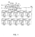
- FIG. 1 is a schematic circuit block diagram showing a circuit for computing SAD in accordance with a preferred embodiment of the invention.
- FIG. 2A is a view showing computation of absolute difference of an image block data and a to-be-compared image block data according to an embodiment of the present invention.
- FIG. 2B illustrates an order of processing 4x4 pixel blocks. We can obtain all SAD values with inputting PM i,j and PS i,j once in the order.
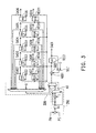
- FIG. 3 is a schematic circuit block diagram showing a circuit for computing SAD according to another preferred embodiment of the invention.
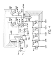
- FIG. 4 is a schematic circuit block diagram showing a circuit for computing SAD according to third preferred embodiment of the invention.
- FIG. 1 is a circuit block diagram showing a circuit for computing SAD according to an embodiment of the present invention.
- a first data PM e.g. an image block data
- a second data PS e.g. a to-be-compared image block diagram comprise series of data.
- the subtracter 111 receives the image block data PM as well as the to-be-compared image block data PS, and then subtracts the image block data PM from the to-be-compared image block data PS or subtracts the to-be-compared image block data PS from the image block data PM so as to output the difference value 112.
- the register 113 is coupled to the subtracter 111, locking the difference value 112 according to the preset timing sequence so as to output the difference value 114.
- the complement circuit 115 is coupled to the register 113 for generating the complement value 116 according to the difference value 114.
- the selective circuit 117 is coupled to the register 113 and the complement circuit 115 for receiving the difference value 114 and the complement value 116 of the difference value 114, and outputting the difference value 114 or the complement value 116 of the difference value 114 which is a positive value as the absolute difference data AD.
- the complement circuit 115 comprises, for example, an inverter 118 and an adder 119.
- the inverter 118 receives and inverses the difference value 114.
- the adder 119 is coupled to the inverter 118 for receiving and adding the inversed difference value 114, and outputting the complement value 116 of the difference value 114.
- the adder ADD 1 receives and adds the absolute difference data AD and the accumulative data 121, and outputs the accumulated result as the sum 122.
- the register REG1 locks the sum 122 according to the preset timing sequence, and outputs the SAD data SAD1.
- the selective circuit SEL1 receives and selects the SAD1 or 0, and outputs the selected data as the accumulative data 121.
- the register REG1 stores the SAD of the 4x4 pixel.
- FIG. 2A The computation of absolute difference of the image block data and the to-be-compared image block data according to an embodiment of the present invention is shown in FIG. 2A.
- the absolute difference circuit 110 receives the image block data PM and the to-be-compared image block data PS.
- the circuit SEL1 select 0 as the output.
- the register REG1 locks the computed result AD ij +0 of the adder ADD1 as the output SAD1.
- the selective circuit SEL1 selects and transmits the SAD1, i.e. AD ij , outputted from the register REG1 to the adder ADD1.
- the register REG1 locks the computed result AD ij +AD i+1j outputted from the adder ADD 1.
- the selective circuit SEL1 selects and transmits the SAD1, i.e. AD ij + ... + AD i+2j+3 , outputted from the register REG1 to the adder ADD1.
- the computation of SAD for the 4x4 pixel is completed.
- the circuit can also be adapted for computing SAD a variety of image block data, and is not limited to 4x4 pixel described above.
- the output terminal of the register REG1 is coupled to a plurality of sets of accumulative circuits SUM2-SUM11.
- the accumulative circuits compute the SAD by accumulating SAD1.
- the accumulative circuits SUM2-SUM11 accumulate the SAD2-SAD11 of the 4x8 (left), 4x8(right), 8x4(top), 8 ⁇ 4(bottom), 8x8, 8x16(left), 8x16(right), 16 ⁇ 8(top), 16x8(bottom) and 16x16 image block data according to the preset timing sequence.
- the number of the accumulative circuits is not fixed. For example, if the SAD for the 4x4, 8x8 and 16 ⁇ 16 image block data are to be simultaneously computed, the accumulative circuits SUM2-SUM5 and SUM7-SUM10 shown in FIG. 1 maybe are not required. If the SAD of the 8x8 image block data is to be computed only, the accumulative circuits SUM2-SUM11 shown in FIG. 1 maybe are not required. By modifying the timing sequence of the selective circuit SEL1 for selecting 0, the register REG1 can output the SAD of the 8x8 image block data. These amendments described above fall within the scope of the present invention.
- FIG. 2B is a schematic view showing a 16 ⁇ 16 image block is split into sixteen 4x4 image blocks, and the number of each 4x4 image block is the processing order.
- the accumulative circuits SUM2-SUM11 are circuits similar to each other. Following is the description of the accumulative circuit SUM 11.
- the accumulative circuit SUM11 comprises an adder, a register and a selective circuit. The operations of the adder, the register and the selective circuit are similar to those of the adder ADD1, the register REG1 and the selective circuit SEL1, respectively. Therefore, detailed descriptions thereof are not repeated.
- the SUM11 compute the SAD of 16x16 image block by accumulating sixteen SAD of 4x4 image block, i.e. SAD1.
- the circuit of the present invention computes SAD for various image block data in a short time. Following is a description concerning the circuit area.
- FIG. 3 is a schematic circuit block diagram showing a circuit for computing SAD according to another embodiment of the present invention.
- the absolute circuit 310 receives the image block data PM and the to-be-compared image block data PS, and outputs the absolute difference data AD.
- the absolute difference circuit 310, the adder ADD1, the register REG1 and the selective circuit SEL1 are similar to the absolute difference circuit 110, the adder ADD 1, the register REG 1 and the selective circuit SEL1 shown in FIG. 1, respectively. Therefore, detailed descriptions thereof are not repeated.
- the selective circuit 320 is coupled between the absolute circuit 310 and the adder ADD1.
- the register REG1 stores the SAD of the 4x4 pixel.
- the outputs, SAD2 to SAD11, are accumulated.
- the circuit can also be adapted for computing SAD of a variety of image block data, and is not only limited to the 4x4 pixel described above.
- the number of the accumulative circuits is not fixed. For example, if the SAD for the 4x4, 8x8 and 16x16 image block data are to be simultaneously computed, the accumulative circuits SUM2-SUM5 and SUM7-SUM10 shown in FIG. 1 maybe are not required. If the sum of absolute difference of the 8x8 image block data is to be computed, the accumulative circuits SUM2-SUM11 shown in FIG. 1 maybe not required. By modifying the timing sequence of the selective circuit SEL1 for selecting 0, the register REG1 can output the sum of absolute difference for the 8x8 image block data. These embodiments described above fall within the scope of the present invention.
- the sequence of the data for the 4x4 pixel is shown in FIG. 2B.
- the registers REG2, REG4, REG6, REG7, REG9, REG11 and REG1 lock the accumulative value 322.
- REG3 and REG1 lock the accumulative value 322.
- the selective circuit 320 selects and outputs SAD4, SAD6, SAD7, SAD9 and SAD 11 to the adder ADD 1 for the adding computations with SAD 1 of the second 4x4 image block data so as to store the accumulative results.
- the register REG4 outputs SAD4 of the first 8x4 image block data. The other data are outputted according thereto. therefore, detailed descriptions thereof are not repeated.
- circuits for sum of absolute difference shown in FIGS. 1 and 3 are novel and have unique features, in that, the circuit shown in FIG. 1 is capable of computing sums of absolute difference of a variety of image block data in a short time and the circuit shown in FIG. 3 has a small circuit area. Following is a description of a circuit having complement features of the circuits shown in FIGS. 1 and 3.
- FIG. 4 is a schematic circuit block diagram showing a circuit for computing sums of absolute difference according to another embodiment of the present invention.
- the absolute circuit 410 receives the image block data PM and the to-be-compared image block data PS, and outputs the absolute difference data AD.
- the absolute difference circuit 410, the adder ADD1, the registers REG1 to REG6 and the selective circuit SEL1 are similar to the absolute difference circuit 310, the adder ADD1, the registers REG1 to REG6 and the selective circuit SEL1 shown in FIG. 3, respectively. Therefore, detailed descriptions thereof are not repeated.
- the adder 430 is coupled to the output terminal of the register REG6, and receives SAD6 so as to perform adding computation with the selected data from the selective circuit 440.
- the register REG6 locks the sum of absolute difference of the 8x8 image block data.
- the adder ADD1 accumulates the SAD6 to the register corresponding thereto by the switching of the selective circuit 440 before the ADD1 completely outputs the sum of absolute difference data of the 4x4 image block data.
- the circuit in this embodiment performs more efficiently though the selective circuit 440 and the adder 430 are added.
Landscapes
- Engineering & Computer Science (AREA)
- General Physics & Mathematics (AREA)
- Physics & Mathematics (AREA)
- Theoretical Computer Science (AREA)
- Signal Processing (AREA)
- Computational Mathematics (AREA)
- Computing Systems (AREA)
- Multimedia (AREA)
- Mathematical Analysis (AREA)
- Mathematical Optimization (AREA)
- Pure & Applied Mathematics (AREA)
- General Engineering & Computer Science (AREA)
- Compression, Expansion, Code Conversion, And Decoders (AREA)
Priority Applications (1)
| Application Number | Priority Date | Filing Date | Title |
|---|---|---|---|
| EP05011730A EP1729518A1 (de) | 2005-05-31 | 2005-05-31 | Schaltung zur Berechnung von Summen absoluter Differenzen |
Applications Claiming Priority (1)
| Application Number | Priority Date | Filing Date | Title |
|---|---|---|---|
| EP05011730A EP1729518A1 (de) | 2005-05-31 | 2005-05-31 | Schaltung zur Berechnung von Summen absoluter Differenzen |
Publications (1)
| Publication Number | Publication Date |
|---|---|
| EP1729518A1 true EP1729518A1 (de) | 2006-12-06 |
Family
ID=35033691
Family Applications (1)
| Application Number | Title | Priority Date | Filing Date |
|---|---|---|---|
| EP05011730A Withdrawn EP1729518A1 (de) | 2005-05-31 | 2005-05-31 | Schaltung zur Berechnung von Summen absoluter Differenzen |
Country Status (1)
| Country | Link |
|---|---|
| EP (1) | EP1729518A1 (de) |
Citations (4)
| Publication number | Priority date | Publication date | Assignee | Title |
|---|---|---|---|---|
| US5717615A (en) * | 1994-12-13 | 1998-02-10 | Thomson Multimedia S.A. | Method for selecting motion vectors and image processing device implementing the said method |
| US5793655A (en) * | 1996-10-23 | 1998-08-11 | Zapex Technologies, Inc. | Sum of the absolute values generator |
| US20010028681A1 (en) * | 2000-01-27 | 2001-10-11 | Choi Sung-Kyu | Motion estimator |
| US20020039386A1 (en) * | 2000-07-13 | 2002-04-04 | Tae-Hee Han | Block matching processor and method for block matching motion estimation in video compression |
-
2005
- 2005-05-31 EP EP05011730A patent/EP1729518A1/de not_active Withdrawn
Patent Citations (4)
| Publication number | Priority date | Publication date | Assignee | Title |
|---|---|---|---|---|
| US5717615A (en) * | 1994-12-13 | 1998-02-10 | Thomson Multimedia S.A. | Method for selecting motion vectors and image processing device implementing the said method |
| US5793655A (en) * | 1996-10-23 | 1998-08-11 | Zapex Technologies, Inc. | Sum of the absolute values generator |
| US20010028681A1 (en) * | 2000-01-27 | 2001-10-11 | Choi Sung-Kyu | Motion estimator |
| US20020039386A1 (en) * | 2000-07-13 | 2002-04-04 | Tae-Hee Han | Block matching processor and method for block matching motion estimation in video compression |
Similar Documents
| Publication | Publication Date | Title |
|---|---|---|
| US6473529B1 (en) | Sum-of-absolute-difference calculator for motion estimation using inversion and carry compensation with full and half-adders | |
| Jridi et al. | A generalized algorithm and reconfigurable architecture for efficient and scalable orthogonal approximation of DCT | |
| Lai et al. | A data-interlacing architecture with two-dimensional data-reuse for full-search block-matching algorithm | |
| KR101578052B1 (ko) | 움직임 추정 장치 및 이를 구비하는 동영상 부호화 장치 | |
| CN101375606A (zh) | 视频编码 | |
| KR100793976B1 (ko) | 움직임 추정 회로 및 그 동작 방법 | |
| US8416856B2 (en) | Circuit for computing sums of absolute difference | |
| US20030118103A1 (en) | Method for performing motion estimation in video encoding, a video encoding system and a video encoding device | |
| Kuo et al. | Polynomial search algorithms for motion estimation | |
| Artieri et al. | A versatile and powerful chip for real-time motion estimation | |
| EP1729518A1 (de) | Schaltung zur Berechnung von Summen absoluter Differenzen | |
| US7804900B2 (en) | Method for fast SATD estimation | |
| Akin et al. | High performance hardware architectures for one bit transform based motion estimation | |
| US20050131979A1 (en) | Apparatus for calculating absolute difference value, and motion estimation apparatus and motion picture encoding apparatus which use the apparatus for calculating the absolute difference value | |
| Renda et al. | Approximate Arai DCT architecture for HEVC | |
| Lee | Low-complexity parallel systolic Montgomery multipliers over GF (2 m) using Toeplitz Matrix-vector representation | |
| Shah et al. | Implementation of sum of absolute difference using optimized partial summation term reduction | |
| Hegde et al. | An efficient hardware realization of diamond search algorithm for motion estimation task in video compression applications | |
| US20040081365A1 (en) | Method and apparatus for adaptive pixel estimation under high error rate conditions | |
| US20030142743A1 (en) | Inverse discrete cosine transform apparatus | |
| KR100359091B1 (ko) | 움직임추정장치 | |
| de Fraga et al. | Design and Analysis of Approximate Hardware Accelerators for VVC Intra Angular Prediction | |
| Liu et al. | High-speed systolic ladder structures for multidimensional recursive digital filters | |
| Lee et al. | An effective successive elimination algorithm for fast optimal block-matching motion estimation | |
| Olivares | Reconfigurable architecture for VBSME with variable pixel precision |
Legal Events
| Date | Code | Title | Description |
|---|---|---|---|
| PUAI | Public reference made under article 153(3) epc to a published international application that has entered the european phase |
Free format text: ORIGINAL CODE: 0009012 |
|
| 17P | Request for examination filed |
Effective date: 20060418 |
|
| AK | Designated contracting states |
Kind code of ref document: A1 Designated state(s): AT BE BG CH CY CZ DE DK EE ES FI FR GB GR HU IE IS IT LI LT LU MC NL PL PT RO SE SI SK TR |
|
| AX | Request for extension of the european patent |
Extension state: AL BA HR LV MK YU |
|
| AKX | Designation fees paid | ||
| STAA | Information on the status of an ep patent application or granted ep patent |
Free format text: STATUS: THE APPLICATION IS DEEMED TO BE WITHDRAWN |
|
| 18D | Application deemed to be withdrawn |
Effective date: 20070213 |
|
| REG | Reference to a national code |
Ref country code: DE Ref legal event code: 8566 |