EP1731632A2 - Substrat aus Nitrid-Halbleiter und Verfahren zu seiner Herstellung - Google Patents
Substrat aus Nitrid-Halbleiter und Verfahren zu seiner Herstellung Download PDFInfo
- Publication number
- EP1731632A2 EP1731632A2 EP06011299A EP06011299A EP1731632A2 EP 1731632 A2 EP1731632 A2 EP 1731632A2 EP 06011299 A EP06011299 A EP 06011299A EP 06011299 A EP06011299 A EP 06011299A EP 1731632 A2 EP1731632 A2 EP 1731632A2
- Authority
- EP
- European Patent Office
- Prior art keywords
- facets
- mask
- gan
- regions
- undersubstrate
- Prior art date
- Legal status (The legal status is an assumption and is not a legal conclusion. Google has not performed a legal analysis and makes no representation as to the accuracy of the status listed.)
- Withdrawn
Links
Images


Classifications
-
- H—ELECTRICITY
- H10—SEMICONDUCTOR DEVICES; ELECTRIC SOLID-STATE DEVICES NOT OTHERWISE PROVIDED FOR
- H10P—GENERIC PROCESSES OR APPARATUS FOR THE MANUFACTURE OR TREATMENT OF DEVICES COVERED BY CLASS H10
- H10P14/00—Formation of materials, e.g. in the shape of layers or pillars
- H10P14/20—Formation of materials, e.g. in the shape of layers or pillars of semiconductor materials
-
- C—CHEMISTRY; METALLURGY
- C30—CRYSTAL GROWTH
- C30B—SINGLE-CRYSTAL GROWTH; UNIDIRECTIONAL SOLIDIFICATION OF EUTECTIC MATERIAL OR UNIDIRECTIONAL DEMIXING OF EUTECTOID MATERIAL; REFINING BY ZONE-MELTING OF MATERIAL; PRODUCTION OF A HOMOGENEOUS POLYCRYSTALLINE MATERIAL WITH DEFINED STRUCTURE; SINGLE CRYSTALS OR HOMOGENEOUS POLYCRYSTALLINE MATERIAL WITH DEFINED STRUCTURE; AFTER-TREATMENT OF SINGLE CRYSTALS OR A HOMOGENEOUS POLYCRYSTALLINE MATERIAL WITH DEFINED STRUCTURE; APPARATUS THEREFOR
- C30B29/00—Single crystals or homogeneous polycrystalline material with defined structure characterised by the material or by their shape
- C30B29/10—Inorganic compounds or compositions
- C30B29/40—AIIIBV compounds wherein A is B, Al, Ga, In or Tl and B is N, P, As, Sb or Bi
- C30B29/403—AIII-nitrides
-
- C—CHEMISTRY; METALLURGY
- C30—CRYSTAL GROWTH
- C30B—SINGLE-CRYSTAL GROWTH; UNIDIRECTIONAL SOLIDIFICATION OF EUTECTIC MATERIAL OR UNIDIRECTIONAL DEMIXING OF EUTECTOID MATERIAL; REFINING BY ZONE-MELTING OF MATERIAL; PRODUCTION OF A HOMOGENEOUS POLYCRYSTALLINE MATERIAL WITH DEFINED STRUCTURE; SINGLE CRYSTALS OR HOMOGENEOUS POLYCRYSTALLINE MATERIAL WITH DEFINED STRUCTURE; AFTER-TREATMENT OF SINGLE CRYSTALS OR A HOMOGENEOUS POLYCRYSTALLINE MATERIAL WITH DEFINED STRUCTURE; APPARATUS THEREFOR
- C30B25/00—Single-crystal growth by chemical reaction of reactive gases, e.g. chemical vapour-deposition growth
- C30B25/02—Epitaxial-layer growth
- C30B25/18—Epitaxial-layer growth characterised by the substrate
-
- C—CHEMISTRY; METALLURGY
- C30—CRYSTAL GROWTH
- C30B—SINGLE-CRYSTAL GROWTH; UNIDIRECTIONAL SOLIDIFICATION OF EUTECTIC MATERIAL OR UNIDIRECTIONAL DEMIXING OF EUTECTOID MATERIAL; REFINING BY ZONE-MELTING OF MATERIAL; PRODUCTION OF A HOMOGENEOUS POLYCRYSTALLINE MATERIAL WITH DEFINED STRUCTURE; SINGLE CRYSTALS OR HOMOGENEOUS POLYCRYSTALLINE MATERIAL WITH DEFINED STRUCTURE; AFTER-TREATMENT OF SINGLE CRYSTALS OR A HOMOGENEOUS POLYCRYSTALLINE MATERIAL WITH DEFINED STRUCTURE; APPARATUS THEREFOR
- C30B29/00—Single crystals or homogeneous polycrystalline material with defined structure characterised by the material or by their shape
- C30B29/10—Inorganic compounds or compositions
- C30B29/40—AIIIBV compounds wherein A is B, Al, Ga, In or Tl and B is N, P, As, Sb or Bi
- C30B29/403—AIII-nitrides
- C30B29/406—Gallium nitride
-
- H—ELECTRICITY
- H10—SEMICONDUCTOR DEVICES; ELECTRIC SOLID-STATE DEVICES NOT OTHERWISE PROVIDED FOR
- H10F—INORGANIC SEMICONDUCTOR DEVICES SENSITIVE TO INFRARED RADIATION, LIGHT, ELECTROMAGNETIC RADIATION OF SHORTER WAVELENGTH OR CORPUSCULAR RADIATION
- H10F77/00—Constructional details of devices covered by this subclass
- H10F77/10—Semiconductor bodies
- H10F77/12—Active materials
- H10F77/124—Active materials comprising only Group III-V materials, e.g. GaAs
-
- H—ELECTRICITY
- H10—SEMICONDUCTOR DEVICES; ELECTRIC SOLID-STATE DEVICES NOT OTHERWISE PROVIDED FOR
- H10P—GENERIC PROCESSES OR APPARATUS FOR THE MANUFACTURE OR TREATMENT OF DEVICES COVERED BY CLASS H10
- H10P14/00—Formation of materials, e.g. in the shape of layers or pillars
- H10P14/20—Formation of materials, e.g. in the shape of layers or pillars of semiconductor materials
- H10P14/22—Formation of materials, e.g. in the shape of layers or pillars of semiconductor materials using physical deposition, e.g. vacuum deposition or sputtering
-
- H—ELECTRICITY
- H10—SEMICONDUCTOR DEVICES; ELECTRIC SOLID-STATE DEVICES NOT OTHERWISE PROVIDED FOR
- H10P—GENERIC PROCESSES OR APPARATUS FOR THE MANUFACTURE OR TREATMENT OF DEVICES COVERED BY CLASS H10
- H10P14/00—Formation of materials, e.g. in the shape of layers or pillars
- H10P14/20—Formation of materials, e.g. in the shape of layers or pillars of semiconductor materials
- H10P14/24—Formation of materials, e.g. in the shape of layers or pillars of semiconductor materials using chemical vapour deposition [CVD]
-
- H—ELECTRICITY
- H10—SEMICONDUCTOR DEVICES; ELECTRIC SOLID-STATE DEVICES NOT OTHERWISE PROVIDED FOR
- H10P—GENERIC PROCESSES OR APPARATUS FOR THE MANUFACTURE OR TREATMENT OF DEVICES COVERED BY CLASS H10
- H10P14/00—Formation of materials, e.g. in the shape of layers or pillars
- H10P14/20—Formation of materials, e.g. in the shape of layers or pillars of semiconductor materials
- H10P14/27—Formation of materials, e.g. in the shape of layers or pillars of semiconductor materials using selective deposition, e.g. simultaneous growth of monocrystalline and non-monocrystalline semiconductor materials
- H10P14/271—Formation of materials, e.g. in the shape of layers or pillars of semiconductor materials using selective deposition, e.g. simultaneous growth of monocrystalline and non-monocrystalline semiconductor materials characterised by the preparation of substrate for selective deposition
- H10P14/272—Formation of materials, e.g. in the shape of layers or pillars of semiconductor materials using selective deposition, e.g. simultaneous growth of monocrystalline and non-monocrystalline semiconductor materials characterised by the preparation of substrate for selective deposition using mask materials other than SiO2 or SiN
-
- H—ELECTRICITY
- H10—SEMICONDUCTOR DEVICES; ELECTRIC SOLID-STATE DEVICES NOT OTHERWISE PROVIDED FOR
- H10P—GENERIC PROCESSES OR APPARATUS FOR THE MANUFACTURE OR TREATMENT OF DEVICES COVERED BY CLASS H10
- H10P14/00—Formation of materials, e.g. in the shape of layers or pillars
- H10P14/20—Formation of materials, e.g. in the shape of layers or pillars of semiconductor materials
- H10P14/27—Formation of materials, e.g. in the shape of layers or pillars of semiconductor materials using selective deposition, e.g. simultaneous growth of monocrystalline and non-monocrystalline semiconductor materials
- H10P14/276—Lateral overgrowth
-
- H—ELECTRICITY
- H10—SEMICONDUCTOR DEVICES; ELECTRIC SOLID-STATE DEVICES NOT OTHERWISE PROVIDED FOR
- H10P—GENERIC PROCESSES OR APPARATUS FOR THE MANUFACTURE OR TREATMENT OF DEVICES COVERED BY CLASS H10
- H10P14/00—Formation of materials, e.g. in the shape of layers or pillars
- H10P14/20—Formation of materials, e.g. in the shape of layers or pillars of semiconductor materials
- H10P14/29—Formation of materials, e.g. in the shape of layers or pillars of semiconductor materials characterised by the substrates
- H10P14/2901—Materials
- H10P14/2907—Materials being Group IIIA-VA materials
- H10P14/2911—Arsenides
-
- H—ELECTRICITY
- H10—SEMICONDUCTOR DEVICES; ELECTRIC SOLID-STATE DEVICES NOT OTHERWISE PROVIDED FOR
- H10P—GENERIC PROCESSES OR APPARATUS FOR THE MANUFACTURE OR TREATMENT OF DEVICES COVERED BY CLASS H10
- H10P14/00—Formation of materials, e.g. in the shape of layers or pillars
- H10P14/20—Formation of materials, e.g. in the shape of layers or pillars of semiconductor materials
- H10P14/29—Formation of materials, e.g. in the shape of layers or pillars of semiconductor materials characterised by the substrates
- H10P14/2901—Materials
- H10P14/2921—Materials being crystalline insulating materials
-
- H—ELECTRICITY
- H10—SEMICONDUCTOR DEVICES; ELECTRIC SOLID-STATE DEVICES NOT OTHERWISE PROVIDED FOR
- H10P—GENERIC PROCESSES OR APPARATUS FOR THE MANUFACTURE OR TREATMENT OF DEVICES COVERED BY CLASS H10
- H10P14/00—Formation of materials, e.g. in the shape of layers or pillars
- H10P14/20—Formation of materials, e.g. in the shape of layers or pillars of semiconductor materials
- H10P14/29—Formation of materials, e.g. in the shape of layers or pillars of semiconductor materials characterised by the substrates
- H10P14/2926—Crystal orientations
-
- H—ELECTRICITY
- H10—SEMICONDUCTOR DEVICES; ELECTRIC SOLID-STATE DEVICES NOT OTHERWISE PROVIDED FOR
- H10P—GENERIC PROCESSES OR APPARATUS FOR THE MANUFACTURE OR TREATMENT OF DEVICES COVERED BY CLASS H10
- H10P14/00—Formation of materials, e.g. in the shape of layers or pillars
- H10P14/20—Formation of materials, e.g. in the shape of layers or pillars of semiconductor materials
- H10P14/32—Formation of materials, e.g. in the shape of layers or pillars of semiconductor materials characterised by intermediate layers between substrates and deposited layers
- H10P14/3202—Materials thereof
- H10P14/3214—Materials thereof being Group IIIA-VA semiconductors
- H10P14/3216—Nitrides
-
- H—ELECTRICITY
- H10—SEMICONDUCTOR DEVICES; ELECTRIC SOLID-STATE DEVICES NOT OTHERWISE PROVIDED FOR
- H10P—GENERIC PROCESSES OR APPARATUS FOR THE MANUFACTURE OR TREATMENT OF DEVICES COVERED BY CLASS H10
- H10P14/00—Formation of materials, e.g. in the shape of layers or pillars
- H10P14/20—Formation of materials, e.g. in the shape of layers or pillars of semiconductor materials
- H10P14/34—Deposited materials, e.g. layers
- H10P14/3402—Deposited materials, e.g. layers characterised by the chemical composition
- H10P14/3414—Deposited materials, e.g. layers characterised by the chemical composition being group IIIA-VIA materials
- H10P14/3416—Nitrides
Definitions
- This invention relates to a nitride semiconductor substrate, which is composed of two-dimensional regularly repeating polygonal-shaped low defect density single crystal regions and a network of defect accumulating regions enclosing and joining the polygonal-shaped low defect density single crystal regions, and a method of producing such a nitride semiconductor substrate.
- a semiconductor substrate is a basic crystal plate on which semiconductor devices are fabricated. It is common sense that good substrates should have complete uniformity of components and structures as a whole.
- the present invention proposes a nitride substrate which has intentionally-introduced non-uniformity to components and structures.
- the nitride substrate proposed by the present invention is different from the conventional semiconductor substrates on this point.
- Nitride semiconductors mean gallium nitride (GaN), aluminum gallium nitride(AlGaN), indium gallium nitride(InGaN) and aluminum nitride (AlN) and indium nitride (InN).
- a group 3-5 nitride semiconductors is a synonym of the nitride semiconductors.
- a substrate is a crystal base board on which devices are produced. A substrate is also called a "wafer".
- Sapphire Al 2 O 3
- Sapphire substrates enable us to make GaN, InGaN or AlGaN or other nitride films thereupon. Sapphire is congenial to the group 3-5 nitrides. Sapphire wafers have been pertinent substrates for blue ray LEDs.
- Vapor phase growth for example, MOCVD
- MOCVD Metal Organic Chemical Vapor phase growth
- Etch pit density which is a measure of dislocations, is very high of the order of 10 10 cm -2 in the films grown on sapphire substrates.
- On-sapphire LEDs have been on the market and in use on a large scale.
- Sapphire lacks natural cleavage.
- Sapphire is an insulator.
- Sapphire has large lattice misfitting to gallium nitride. Lack of cleavage prohibits device makers from dividing a processed wafer into individual device chips by natural cleavage.
- Sapphire wafer should be divided into chips by mechanical dicing, which invites a low yield and causes high costs.
- Laser diodes (LDs) made on sapphire substrates have an additional drawback of the impossibility of making resonator mirrors by natural cleavage.
- GaN crystals for the substrates of GaN-type light emitting devices has been ardently desired. It has been difficult to produce gallium nitride (GaN) single crystal substrates of high quality with low dislocation density (EPD). No melt can be prepared by heating GaN, AIN or InN polycrystals. Conventional Czochralski method and Bridgman method are inapplicable to making GaN crystal.
- GaN gallium nitride
- An MOCVD (metallorganic chemical vapor deposition) method enables us to produce a thin gallium nitride film on a sapphire ( ⁇ -Al 2 O 3 ) undersubstrate.
- the MOCVD method is inherently a technique of making thin films.
- the MOCVD produces a GaN thin film by supplying a heated sapphire undersubstrate with an organic metal gas of Ga, for example, TMG (trimethylgallium) or TEG(triethylgallium) and ammonia (NH 3 ) gas.
- TMG trimethylgallium
- TEG(triethylgallium) and ammonia (NH 3 ) gas Direct deposition of GaN film on the sapphire undersubstrate causes large dislocation density.
- An ELO method epipitaxial lateral overgrowth is employed for decreasing dislocations on films grown on the undersubstrate.
- the ELO method forms a mask M having plenty of small isolated windows on an undersubstrate and grows GaN on the ELO-masked undersubstrate.
- a part covered with the mask M is a wide continual part in the ELO.
- the masked part of the undersubstrate is called a covered part T from now.
- Extra parts of the substrate which are not covered with the mask are called exposed parts ⁇ for clearly discriminating from the covered part.
- the term of "covered” or "exposed” is defined only by the fact that the mask covers or uncovers.
- the name of exposed parts of the undersubstrate shall be maintained until the exposed parts have been concealed with growing GaN films. In this description the exposed parts II and the covered parts T will be used for indicating unmasked and masked parts of an undersubstrate.
- Fig.20 demonstrates an ELO-mask M and an undersubstrate S covered with the ELO-mask M for ELO-growth.
- the ELO mask is prepared by depositing a SiO 2 film overall upon an undersubstrate and boring tiny windows by photolithography and etching.
- An exposed part ⁇ is a tiny isolated window in the ELO mask.
- the covered part T area S1 is absolutely wider than the exposed part ⁇ area S2 (S1 >> S2).
- the mask has a function of impeding crystal growth. Crystal growth starts on the exposed parts ⁇ . Crystal grains fill the exposed parts and enlarge upward. Dislocations also extend upward in parallel with the crystal growth. The crystal runs up onto the mask and extends in horizontal directions on the mask. Dislocations also extend in the horizontal directions on the mask.
- the crystals are unified and make a flat uniform C-plane.
- the horizontal collision reduces dislocations.
- the ELO grows a crystal film with maintaining the flat C-plane after the horizontal collision.
- Fig.21 demonstrates the ELO growth keeping a flat C-plane top after the unification of crystals on the mask. In practice, it is difficult to maintain the flat C-plane top of the GaN film.
- the growing conditions shall be always controlled so as to prohibit hills or pits from occurring by watching the surface of the growing crystal.
- the ELO is a technique for decreasing dislocations by horizontal collision at an early stage of growth.
- the ELO is effective in the growth of thin films with a thickness of 0.1 ⁇ m to 3 ⁇ m. 1 ⁇ m to 4 ⁇ m thick GaN or InGaN films
- ELO-grown on sapphire substrates have dislocation density of 10 9 cm -2 to 10 11 cm -2 . Congeniality of sapphire to GaN or InGaN enables the ELO-grown LEDs to emit light without degeneration.
- the ELO method is scarcely effective in the crystal growth of thick crystals. Thick GaN crystal made by the ELO, which has high dislocation density of 10 9 cm -2 to 10 11 cm -2 , will exfoliate from undersubstrates. Even if the thick GaN crystal would not come off undersubstrates, the dislocation density ranging from 10 9 cm -2 to 10 11 cm -2 is too high. New technique other than the ELO is required to make thick GaN substrate crystals.
- the Inventors have contrived a new method, which can be called a "facet growth method", for producing thick, low-dislocation GaN crystal substrates.
- a substrate is a basic board on which devices are fabricated.
- a substrate is sometimes called a "wafer”.
- the facet growth method has a history of improvements which have been done by the Inventors of the present invention. There have been three preceding facet growth methods. All the three preceding facet growth methods are explained.
- Japanese Patent Laying Open No.2001-102307 proposes a method of growing GaN crystals by making many facets and facet pits on a surface of the growing crystal, on purpose not burying the pits and maintaining the facets till the end of GaN crystal growth.
- Fig.22 denotes an undersubstrate S for the facet growth.
- the undersubstrate has no mask.
- Vapor phase growth inherently produces facets ⁇ and facet pits.
- Conventional vapor phase growth methods had tried to eliminate the facets and to make a flat C-plane on the top by controlling conditions of growth. On the contrary, the facet growth method does not bury the facet pits but maintains the facets and facet pits.
- Facet growth method contradicts the conventional methods, which may be called a "C-plane growth" method.
- Facets ⁇ denote crystallographic planes having low Miller indices (khmn).
- Low Miller indices mean indices k, h, m and n are 0, ⁇ 1, ⁇ 2 or so.
- a set of facets form a pit of facets.
- Fig.23 shows a GaN film having facet pits on a surface which is made by the facet growth method.
- a facet pit is an assembly composed of six facets or twelve facets. Six or twelve facets make inverse hexagonal cones or inverse dodecagonal cones.
- Plenty of facet pits having a variety of shapes and sizes are randomly dispersed on the GaN surface.
- the GaN crystal grows upward in the direction of the c-axis as a whole. The average direction of growth is the c-axis direction. But in the facet pits, crystals grow in inner slanting directions normal to the facets. Dislocations on the facets extend in the inner slanting directions normal to the facets, and come up to and assemble to boundaries of the facets.
- the dislocations further come up to the bottom of the pits. Many dislocations converge to the bottom of the pits and form a linear defect hanging from the bottom of the facet pit. Dislocations are continual strings which are not easily vanished. Dislocations lying on the facets are pulled to the bottom of the facet pits. Then dislocations in other parts except the pit bottom are reduced. Low dislocation density regions are produced below the facets.
- the facet growth method intentionally produces random facets by controlling the conditions of growth. The facet pits attract, absorb and arrest dislocations at the pit bottoms. A variety of sizes of pits are dispersed at a variety of positions on the C-plane surface at random. The first method is called a "random facet growth" method.
- the random facet growth method has drawbacks.
- the GaN crystal prepared by the method which has defects (dislocations) dispersing on surfaces at random, is not preferable to make devices thereon.
- Such drawbacks degrade the random facet growth method.
- Japanese Patent Laying Open No.2003-165799 Japanese Patent Application No.2002-230925 ) proposed a GaN vapor phase growing method of spotting an undersubstrate with isolated round dot masks for predetermining the positions of facet pits with accuracy.
- Fig.24 denotes an undersubstrate S provided with dispersed isolated small dot masks S.
- the area S1 of covered parts T is far narrower than the area S2 of exposed part ⁇ (S 1 ⁇ S2).
- the relation is inverse to the ELO method.
- S 1 ⁇ S2 is always valid in facet growth methods.
- the facet growth method differs from the ELO in the relation.
- a mask pitch ( ⁇ 100 ⁇ m) of the facet growth method is far longer than the window pitch ( ⁇ 1 ⁇ m) of the ELO method.
- Crystals begin to grow on the exposed part ⁇ .
- the crystals growing on the exposed parts ⁇ couple together and form a flat C-plane as a top surface.
- the mask has a function of impeding and delaying crystal growth.
- a start of growing on the masks is retarded.
- Delay of the crystal growth on the masks M makes facet pits having bottoms coinciding with the isolated masked parts Y.
- Facets are crystallographical planes slanting to the C-plane.
- the facet growth method does not bury facet pits and maintains the facet pits till the end of the growth.
- the facets grow in directions of normals of the facets.
- Dislocations extend in parallel to the growing directions. Slanting growth of a facet sweeps dislocations D lying on the facet to boundaries of facets. The facet slanting growth lowers the dislocations along the boundaries and assembles the dislocations to the pit bottom. High density of dislocations are gathered at the parts just above the masks M. All dislocations are swept away from the facets, are lifted down and are gathered to the pit bottoms above the masks M by the facet growth. In reality dislocations do not lower or lift down but rise upward. Since the standpoint of observation is rising at the speed of the C-plane growth, the dislocations in the facet pits seem to go down.
- the parts above the masks M become defect accumulating regions H. Since the defect accumulating regions H attract, absorb, arrest and accommodate plenty of dislocations, neighboring parts below the facets on the exposed parts become low dislocation density. The regions are called "low defect density single crystal regions Z".
- a crystal out of the pits maintains a flat C-plane top surface and grows upward on the expose part ⁇ . Since dislocations in the part are deprived of the facets, the crystals are also low dislocation density and single crystals.
- the part is called a "C-plane growth region Y".
- the facet-grown crystal has a concentric structure of "HZY".
- Fig.25 demonstrates a facet-growing crystal on an undersubstrate S.
- Y has a continual plateau of the C-plane top.
- Z has facets ⁇ .
- H is a facet pit bottom concealed by Y in the Figure. Since the facets are maintained throughout the growth, the final crystal ingot made by the facet growth method has a rugged surface with many concavities.
- the GaN ingot is sliced in a plane parallel to the C-plane. As-cut GaN wafers are obtained. Both surfaces are polished. Mirror wafers are prepared. A GaN mirror wafer is transparent like a glass plate.
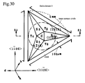
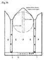
- Fig.26 shows a plan view of a GaN mirror wafer which has the concentric "HZY" structure. Cathode luminescence observation discriminates Y, Z and H. Y, A and H are regions piercing from the top to the bottom of the wafer. The positions of H coincide with the positions of the masks Y. The regions Z coincide with the facets. The region Y coincides with the C-plane top in Fig.25. Z and Y are formed on the exposed part ⁇ . This is called a dot-type facet growth method, since isolated small dot masks are dispersed for making isolated facet pits.
- the dot-type facet growth method produces conical facet pits above the dot masks. Dislocations are absorbed and arrested at the bottoms of the pits. An assembly of dislocations forms a defect accumulating region H at the pit bottom above the mask. Once arrested dislocations are not released from the defect accumulating regions H formed above the masks.
- An advantage is the occurrence of the low defect density single crystal regions Z below the facets on the exposed part.
- the dot-type facet growth method disperses isolated dot masks on the undersubstrate and allows the dot masks to make concentric facet pits. A wide extra space, which corresponds to Y, is left untouched out of the facet pits. The function of the facets of reducing dislocations is insufficient in the C-plane growth region Y.
- the C-plane growth region (Y) has still many dislocations.
- the C-plane region Y has high electric resistance.
- the dot-facet growth is not favorable for making high conductive n-type GaN substrates.
- Anther problem is that existence of the defect accumulating regions H prevents device makers from making a plurality of equivalent devices on the same conditions.
- the random-type facet growth method and the dot-type facet growth method had been invented by the same Inventors as the present invention.
- Japanese Patent Laying Open No.2003-183100 has proposed another facet growth method of covering an undersubstrate with a mask having a plurality of parallel straight covering stripes, growing gallium nitride on the stripe masked undersubstrate, forming parallel straight-extending facetted hills on parallel exposed parts ⁇ , forming parallel straight-extending valleys on the covered stripe parts T, pulling dislocations on the facets of the hills to the valleys and attracting/accumulating/arresting the dislocations in regions H formed at the bottoms of the valleys above the stripe covered parts ⁇ .
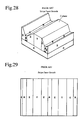
- Fig.27 demonstrates an undersubstrate S provided with parallel straight mask stripes M.
- the numbers of covered parts T and the exposed parts are same. But the area S1 of the covered parts T is far narrower than the area S2 of the exposed parts ⁇ (S1 ⁇ S2). There are several tens of stripes T and several tens of exposed parts II on an undersubstrate, although only two stripes are depicted.
- the masks have a function of prohibiting crystal growth. Vapor phase crystal growth starts on the wide exposed parts II. Parallel crystal hills with side facets are formed on the exposed parts II. After the formation of the facet hills on the exposed parts II, crystal growth starts on the covered parts T. Differences of starting times and growing speeds make parallel facet hills on the exposed parts ⁇ and V-grooves on the stripe covered parts T of GaN crystals.
- Fig.28 demonstrates the hill/valley structure of a growing crystal.
- the bottoms of the V-valleys coincide with the covered (masked) parts ⁇ .
- Reciprocal slanting walls appear on the exposed parts ⁇ .
- the two slanting walls are facets ⁇ .
- the hill or V-groove has only two facets.
- the hill/valley structure is different from the dot-type facet pit having six or twelve facets in the point.
- the facet growth method does not bury the V-grooves but keeps the hill/valley structure. Since crystals grow in the directions normal to the facets, dislocations extend in slanting directions normal to the facets. Dislocations existing on the facets slide from the facets, fall in the valleys and converge at the bottoms of the valleys. Dislocations lying on the facets are attracted and arrested to the bottoms. The valley bottoms become defect accumulating regions H. Crystals growing below the facets become low dislocation density single crystals. The bottom defect accumulating region H is sandwiched by low dislocation single crystal regions Z and Z. The C-plane growth region Y lies aside of Zs. A parallel-extending periodic structure of ... HZYZHZY...
- This facet growth method has an advantage of making low dislocation density single crystal regions Z in a shape of linearly extending stripes.
- the linearly extending Z is favorable for making devices on the GaN substrate.
- Fig.28 demonstrates a facet-growing GaN crystal having valley bottom defect accumulating regions H, low dislocation single crystal regions Z covered with inclining facets, and C-plane growth tops.
- the stripe facet method can eliminate C-plane regions Y by narrowing mask pitch p and composing V-hill/valleys only of facets.
- Narrow mask pitches p (p ⁇ 800 ⁇ m) less than 800 ⁇ m have the possibility of extinguishing C-plane regions.
- the stripe mask pitch described in 3 Japanese Patent Laying Open No.2003-183100 should be less than 2mm (p ⁇ 2000 ⁇ m).
- Another drawback is a tendency of break and split of wafers because of the parallel stripes of Hs, Zs and Ys. This is named “stripe facet growth" method, since H, Z and Y are all parallel stripes.
- the dot facet growth method proposed by 2 Japanese Patent Laying Open No.2003-165799 makes regularly distributing isolated dots of Hs and circular Zs concentrically around the isolated Hs by using dot masks (S 1 ⁇ S2).
- the stripe facet growth method proposed by 3 Japanese Patent Laying Open No.2003-183100 makes a parallel structure of HZYZHZYZH... by using parallel stripe masks (S 1 ⁇ S2).
- the stripe facet growth method proposed by 3 Japanese Patent Laying Open No.2003-183100 is useful for making low dislocation density GaN substrate crystals. However, there are still some problems to be solved.
- a purpose of the present invention is to solve the difficulties above-described.
- the present invention proposes another facet growth method which further lowers dislocation density of GaN substrates, raises emission efficiency of LEDs fabricated on the GaN substrates and divides an epitaxial GaN wafer into larger sized chips by natural cleavage instead of dicing.
- the present invention proposes a network mask facet growth method for forming a set of closed loop masked parts T with definite widths on an undersubstrate S and growing nitride semiconductor crystals on the network masked undersubstrate.
- Nitride semiconductor crystals which first grow on exposed parts ⁇ and second grow on mask covered parts T. There is time lag between the two parts ⁇ and T. As a result, the crystals grown on the covered parts T are lower than facet hills formed the exposed parts ⁇ .
- Dislocations D located in slanting surfaces (facets ⁇ ) of the convex-type facet hills slide from the slanting facet surfaces ⁇ and gather round the covered parts T with the growing of nitride semiconductor crystals.
- the dislocations D assemble in and form defect accumulating regions H just above the covered parts T. Since the facets ⁇ grow in normal directions, the dislocations D caused in the facet parts ⁇ just above the exposed parts ⁇ slide off the facets ⁇ and are captured and held by the defect accumulating regions H.
- the closed loop covered parts T produce closed defect accumulating regions H thereupon.
- the closed defect accumulating regions H act as dislocation attracting/assembling/arresting positions. Once arrested dislocations never escape from the closed defect accumulating regions H.
- Other parts growing within the exposed parts ⁇ neighboring the closed defect accumulating regions H become low dislocation density single crystals.
- the parts growing in the exposed parts ⁇ under the facets are called low defect density single crystal regions Z. Every one of the facetted growing low defect single crystal regions Z is fully enclosed by closed looped defect accumulating regions H. Surrounding defect accumulating regions H pull out dislocations from the single crystal region Z in all directions.
- the reduction of dislocations is far more conspicuous than the former facet growth methods - random facet, dot facet and stripe facet methods.
- the former facet growth methods proposed by the present inventors failed in fully enclosing the low defect single crystal region with closed loop defect accumulating/arresting regions H.
- a flat region which maintains a top C-plane surface, appears at the center of the low defect density single crystal region Z. Appearance or disappearance of the flat top regions depends upon the size of a closed loop or growth conditions.
- the flat top regions are called C-plane growth regions Y.
- the C-plane growth regions Y are also low defect density and single crystals having the same orientation as the surrounding facetted single crystal regions Z.
- the C-plane growth regions Y have electric conductivity higher than the surrounding facetted single crystal regions Z.
- Existence of the C-plane growth regions Y is sometimes an obstacle for making low resistance n-type GaN substrates. Controlling the size of a closed loop mask Y and the growth conditions enables the present invention to reduce or vanish the C-plane growth regions Y.
- the present invention produces closed loop defect accumulating regions H which fully enclose the facetted single crystal regions Z and rid the faceted regions Z of dislocations via the whole boundaries.
- the closed loop defect accumulating regions H succeed in powerfully attracting dislocations out of the facetted single crystal regions Z and in permanently arresting the dislocations. Allover extraction of dislocations from the faceted single crystal regions Z further lowers dislocation density of the closed loop enclosed regions Z. This is a big advantage of the present invention.
- the defect accumulating regions H which are regions accommodating dislocations, become a single crystal having a c-axis fully inverse to the c-axis of the surrounding single crystal regions Z (and Y). This is called an "orientation-inversion single crystal" or "polarity-inversion single crystal".
- Grain boundaries K are made by the orientation inversion between the defect accumulating regions H and the facetted single crystal regions Z. The orientation inversion boundaries K powerfully arrest dislocations and never release the dislocations.
- the defect accumulating regions H become polycrystals.
- grain boundaries K are yielded between the defect accumulating regions H and the inner single crystal regions Z (and Y).
- the grain boundaries prevent once arrested dislocations from escaping into the faceted single crystal regions Z.
- the fact means that clear grain boundaries K are formed between the defect accumulating regions H and the neighboring single crystal regions Z. These are crystal grain boundaries. The dislocations once coming in the defect accumulating regions H are unable to go into the faceted single crystal regions Z.
- the defect accumulating region H has a definite width T' and grain boundaries K and K sandwich the defect accumulating region H.
- the interval between two parallel boundaries K and K is a width T' of the defect accumulating regions H.
- Endowment of a definite width T' to the defect accumulating region H is easily realized by providing the closed loop mask T with a definite width T at the first stage of making the mask pattern on the undersubstrate S.
- the defect accumulating region width T' is smaller than the masked width T (T' ⁇ T).
- the ratio of T'/T depends upon the thickness of the mask M. T' is nearly in proportion to T. T'/T is 0.8 to 0.9 in many cases.
- the width T of the closed loop mask T determines the width T' of the defect accumulating region H which will be formed upon the mask.
- the present invention insists on a closed looped mask, closed loop boundaries K and closed looped defect accumulating regions H.
- Such a mask pattern having repetitions of a basic unit shape in two dimensions should be convenient to device fabrication. Repetitions of a basic unit shape give a network to the mask. Repetitions of the same basic unit shape enable the device makers to produce plural identical devices with the basic unit shape. It is allowable for masks to have such a network pattern arranging many basic circles or ellipsoids aligning in nearly outer contact with neighboring ones.
- the circle or ellipsoid mask will make repetitions of circles or ellipsoids of defect accumulating regions H which can reduce dislocations in neighboring single crystal regions Z. Circles and ellipsoids are allowable for a basic unit shape of a network mask.
- Polygonal unit shapes are required to allow repetitions of a basic shape to cover a two dimensional space without extra margin.
- Probable basic shapes are restricted to equilateral triangles, squares, rectangles, lozenges, parallelograms, trapezoids and so on for covering a two dimensional space with identical basic shapes.
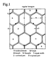
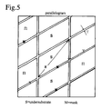
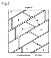
- Figs.1 to 6 are examples of a basic unit shape of a closed loop network mask M.
- the covered parts are denoted by T.
- the exposed parts are denoted by ⁇ .
- Gallium nitride and similar nitride semiconductor crystals take hexagonal system.
- a single crystal plate with a C-plane top has typical directions ⁇ 10-10>, which include three equivalent directions meeting at 120 degrees, and directions ⁇ 11-20>, which include three equivalent directions meeting at 120 degrees.
- Cleavage planes are indicated by ⁇ 10-10 ⁇ .
- ⁇ khmn ⁇ is a collective expression of planes.
- (khmn) is an individual expression of a plane.
- ⁇ khmn ⁇ includes all the individual planes which are obtained from (khmn) by the symmetry operations allowed by the crystal.
- ⁇ khmn> is a collective expression of directions. [khmn] is an individual expression of a direction.
- ⁇ khmn> includes all the individual directions which lead to [khmn] by symmetry operations allowed by the crystal. Since nitride semiconductor crystals have no inversion symmetry, ⁇ khmn ⁇ planes differ from ⁇ -k-h-m-n ⁇ planes. [khmn] denotes an outward normal standing on (khmn). The length of the normal [khmn] is given by a reciprocal of a plane spacing. ⁇ 11-20> direction is parallel to ⁇ 1-100 ⁇ plane. The crystal is easily cleaved along ⁇ 11-20> direction.
- One of the sides of the polygons of a closed loop mask can be determined to be parallel with ⁇ 11-20> direction or ⁇ 10-10>direction of the undersubstrate for giving a definite orientation to facet hills. Otherwise, a side of the mask polygons can be inclined at a definite angle to ⁇ 11-20> or ⁇ 10-10>direction. If a side of the polygon mask coincides with the cleavage plane, facet hills grown within the mask polygon can be separated by cleaving along the side. However, the substrates made by the present invention have non-uniformity of the defect accumulating regions H made on the network.
- the defect accumulating regions H which are peripheries of chips, are corroded away.
- the substrate is divided into chips by the hot KOH/NaOH etching. It is not indispensable for chip-separation to equalize the sides to the cleavage planes.
- Fig.7 plan views
- Fig.8 vertical sectioned views
- Fig.7 plan views
- Fig.8 vertical sectioned views
- the network facet growth method of the present invention is applicable to all the closed loop masks denoted by Figs.1 to 6.
- the facet growth method of the present invention will be explained by citing a regular hexagonal network mask shown by Fig.1.
- Fig.8(1) corresponds to a vertically-sectioned view of the process of forming the regular hexagonal network mask.
- the regular hexagonal network mask is formed on a undersubstrate S.
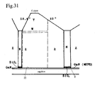
- An upper surface of the undersubstrate S is divided into exposed parts ⁇ and covered parts T.
- Vapor phase growth of nitride semiconductors creates nitride nuclei selectively on the exposed parts ⁇ of the undersubstrate and starts crystal growth on ⁇ .
- nitride semiconductors GaN, InGaN, InN, AIN, AlGaN and so on
- nitride nuclei selectively on the exposed parts ⁇ of the undersubstrate and starts crystal growth on ⁇ .
- T Hexagonal crystal cones are produced on ⁇ .
- the hexagonal cone protrusions seem hills.
- the flat tops of the protrusions are C-planes.
- the hexagonal cones have slanting facets ⁇ at edges being in contact with T.
- the protrusions on ⁇ are called facet hills ⁇ .
- Fig.7(1) and Fig.8(2) demonstrate the creation of facet hills on ⁇ .
- Dislocations extend in a vertical direction in the facet hills from bottom to top, because dislocations are mainly yielde
- Fig.7(2) shows facet hills ⁇ with narrow c-planes on tops. No crystal is born on the masked parts T yet. Sometimes C-planes remain till the end. Other times C-planes perfectly vanish. Non-C-plane crystals are preferable.
- Fig.8(3) demonstrates sharp facet hills ⁇ without C-planes. Pinnacled face hills ⁇ build an ideal crystal.
- the facet hill is composed of six facets ⁇ .
- the six facets aggregate at tops.
- the facet hill is a regular hexagon cone occupying ⁇ .
- Dislocations D expand upward in the facet hills. Top ends of dislocations meet with facets ⁇ with slanting angles. Inclination angles of the facets are determined by plane indices from about 40 degrees to 60 degrees.
- the facet hills ⁇ fill ⁇ in Fig.8(3). The facet hills can dilate no more on ⁇ .
- the crystal growth further proceeds.
- the crystal hills override the masked parts ⁇ .
- Crystal growth starts on the masks ⁇ .
- Facet growth method tries not to bury the facets ⁇ and to maintain the facets ⁇ till the end. Growth of facets ⁇ can be no more vertical, because the slanting facets should be kept.
- Facets grow in the slanting directions vertical to the facets. Facets extend in normals standing on the facets in the facet-growth.
- Dislocations D accompany the facet growth in the normal directions. As shown in Fig.7(3) and Fig.8(4), dislocations D change progressing directions from the vertical to outward slants. Accompanying the facet growth, dislocations extend in outer slanting directions.
- a further facet growth excludes threadlike dislocations out of the facets to regions above ⁇ . Excluded dislocations enter ⁇ from both sides, aggregate with each other above ⁇ and make a bundle of dislocations on the masked parts ⁇ . The aggregated dislocations make defect accumulating regions H on the masked parts ⁇ . Dislocations rarely extinguish and rarely arise in an ordinary growth. Dislocations are attracted, arrested in the defect accumulating regions H on ⁇ . Dislocations in other regions below the facets on ⁇ decrease. The other regions below the facets on ⁇ become low defect density regions. Being low defect density and single crystal, the other regions below the facets on ⁇ are named "low defect density single crystal regions" Z.
- Dislocations are yielded by a variety of irregularities. Most of the dislocations are made at the beginning of crystal growth on the undersubstrate. The crystal is grown in c-axis direction as a whole. Many dislocations have group 3 atoms and nitrogen atoms in reverse positions. Such dislocations assemble to defect accumulating regions H on ⁇ . In many cases, the defect accumulating regions H become single crystals having a downward direction c-axis. In the case, the defect accumulating regions H are single crystals having inverse orientation. The inverse-orientation single crystals are the optimum mode of the defect accumulating regions H. Grain boundaries K are surely born between the inverse defect accumulating regions H and the surrounding low defect single crystals Z and Y. When dislocations are once arrested and accumulated in the defect accumulating regions H, the boundaries K prevent the dislocations from releasing again. The boundaries K arrest the dislocations within the defect accumulating regions H.
- the defect accumulating regions H become polycrystals.
- grain boundaries K are produced between the polycrystalline defect accumulating regions H and the surrounding single crystal regions Z and Y. Boundaries K and K enclose the polycrystalline defect accumulating regions H. Once arrested dislocations are not easily released. The function of confinement of the boundaries K enclosing the polycrystalline H is weaker than that of the boundaries K enclosing the orientation-inverse H.
- Fig.9 is a partially sectioned perspective view of a crystal produced by the facet growth method.
- the surface is occupied by plenty of polygon cone facet hills ⁇ with slanting walls of facets and polygon network bottoms. Sometimes flat parts remain at tops of the facet hills.
- the crystal contain low defect density single crystal regions Z following the facets ⁇ on ⁇ , C-plane growth regions Y following the C-plane tops on ⁇ and defect-accumulating regions H following the network bottoms on masked parts ⁇ . Some samples lack C-plane growth regions Y.
- As-cut GaN wafers are obtained by slicing such a rugged convex/concave GaN crystal ingot in parallel with the C-plane.
- GaN mirror wafers are made by polishing both surfaces of the as-cut wafer.
- Fig.10 shows the structure of a GaN mirror wafer.
- the GaN mirror wafer is not homogeneous but inhomogeneous.
- GaN wafer has an inner structure.
- GaN is transparent like a glass plate.
- the cathode luminescence enables us to observe the inner structure composed of hexagonal low defect density single crystal regions Z extending from bottom to top, a network defect accumulating region H extending from bottom to top and boundaries K between Z and H. This sample lacks C-growth regions Y. Sometimes C-plane growth regions Y remain at the center of Z.
- the width T of the closed loop masked parts ⁇ causing the defect accumulating regions H is 0.05mm to 0.3mm.
- the width T' of the defect accumulating regions H formed on the closed loop mask is slightly narrower than T (T>T').
- T 0.05mm to 0.3mm
- T is smaller than 0.05mm, faint defect accumulating regions H or no defect accumulating regions H are produced on too narrow mask. If the mask width T exceeds 0.3mm, the width T' of defect accumulating regions exceeds 0.2mm.
- the defect accumulating regions H are useless for making devices. Wide defect accumulating regions raise the cost of devices.
- the upper limit of T is 0.3mm.
- More favorable mask width T is 0.05mm to 0.2mm. More favorable width of the defect accumulating region H formed on the mask is 0.03mm to 0.1mm. A narrow mask width reduces the area of defect accumulating regions H and decrease cost of making the substrates.
- the defect accumulating regions H and the boundaries K should be closed loops.
- a low defect density single crystal region Z is enclosed by the closed loop.
- An allowable range of the closed loop shape should be defined.
- L2 is the longest distance from the closed loop to the center of gravity of the low defect density single crystal region Z.
- L1 is the shortest distance from the closed loop to the center of gravity of the low defect density single crystal region Z.
- the ratio L2/L1 should be less than 5 (1 ⁇ L2/L1 ⁇ 5). The restriction gives a clear distinction of the present network facet growth from the former-invented stripe facet growth.
- the ratio of a longer side to a shorter side should be less than five (1 ⁇ L2/L1 ⁇ 5).
- the ratio L2/L1 2 satisfies the requirement of 1 ⁇ L2/L1 ⁇ 5.
- the ratio of longer/shorter sides should be less than 4.68.
- the ratio L2/L1 2 satisfies the requirement of 1 ⁇ L2/L1 ⁇ 5.
- the ratio L2/L1 1.16 satisfies the requirement of 1 ⁇ L2/L1 ⁇ 5.
- the maximum diameter of the closed loop boundaries K for making defect accumulating regions H shall be 0.1mm to 20mm.
- the maximum diameter is defined as the maximum of the distances between two points on the boundaries K. Since a boundary is two dimensional closed loops, the maximum value of distances between two points does exist.
- the value shall be defined as the maximum diameter.
- the value means the maximum of the diameters of the low defect density single crystal regions Z. Boundaries less than a 0.1 mm diameter are capable of reducing dislocations. Since the defect accumulating region closed loops have widths T' of 0.03mm to 0.2mm, economical loss accompanies small boundaries K less than 0.1mm diameter.
- the maximum diameter of the closed loop boundaries K shall be 0.1 mm to 5.0mm.
- the aforedescribed random-type facet growth ( Japanese Patent Laying Open NO.2001-102307 ) and dot-type facet growth ( Japanese Patent Laying Open NO.2003-165799 ) produce cavities, holes or pits composed of facets.
- the pits dispersed on a flat C-plane are assembles of facets. Inclinations of the facets take dislocations in and arrest dislocations at the pit bottoms.
- convexes and concaves of the present invention is reverse to two preceding facet-growth methods.
- the defect accumulating regions H give a standard of height.
- What facets construct is convex facet hills ⁇ embossed on exposed parts ⁇ .
- the facet hills protrude upward from the defect accumulating regions H.
- a facet hill ⁇ grows in a closed loop of the defect accumulating region H.
- the maximum height of the facet hill ⁇ depends upon the breadth of the closed loop boundary K.
- An increment of the closed loop of the defect accumulating region H can increase the maximum height of the facet hills ⁇ . As long as the facets are maintained, the facets keep the function of conveying dislocations from higher parts to lower parts till the closed loop defect accumulating regions H.
- the closed loop defect accumulating regions H attract dislocations from the facet hills. Dislocations within the outlines are decreased by making them pulled radially from all the directions of the closed looped H.
- the present invention differs in the points from other facet pit methods of 1 Japanese Patent Laying Open No.2001-102307 and 2 Japanese Patent Laying Open No.2003-165799 .
- Convex facet hills ⁇ highly protrude on ⁇ .
- Tall, high facets sweep dislocations out of the facet hills ⁇ to ⁇ .
- the dislocation reduction effect pervades innermost parts of the low defect density single crystal regions Z on ⁇ .
- 3 Japanese Patent Laying Open No.2003-183100 has an intermediate character between the concave facet pits of 1 Japanese Patent Laying Open No.2001-102307 or 2 Japanese Patent Laying Open No.2003-165799 and convex facet hills of the present invention.
- Stripe parallel facets of 3 Japanese Patent Laying Open No.2003-183100 are composed of parallel V-grooves and A-roofs.
- the parallel groove/roof structure is neither convex nor concave.
- the stripe mask method making parallel grooves and roofs has an intermediate.
- a V-groove is accompanied by two facets on both sides. Dislocations included in the facets slide down and penetrate into the bottoms of the V-grooves.
- Dislocations are pulled only in two directions vertical to the extension of the parallel V-grooves and A-roofs. Dislocation pulling force and dislocation arresting force are still weak and insufficient in the stripe facet method 3.
- the present invention which is an improvement of the facet growth methods, makes convex facet hills ⁇ , excludes dislocations on ⁇ outward along steep facets in all directions, gathers dislocations into the network closed loop defect accumulating region H enclosing ⁇ and arrests dislocations in the network closed loop H.
- the closed loop H enables the present invention to reduce EPD in facet growth parts to less than 1 ⁇ 10 6 cm -2 .
- the present invention has an excellent strong point of chip-separation by corroding and eliminating the network defect accumulating region H by wet etching or dry-etching in addition to the advantage of reduction of dislocations in the low defect density single crystal regions Z.
- the chip-separation from processed wafers can dispense with cutlery in the present invention. It is very difficult for mechanical cutlery to cut a processed wafer to triangle chips, hexagon chips or other non-rectangle chips. Etching of the network H enables the present invention to divide a processed wafer into arbitrary shapes of chips. This is a conspicuous merit of the present invention.
- Nitride semiconductor crystal are grown on an undersubstrate having a masked part ⁇ and exposed parts ⁇ by making a network closed loop mask. Facet hills with dislocations ⁇ are grown on the exposed part ⁇ A defect accumulating region H is produced on the network closed loop ⁇ .
- the defect accumulating region H encloses facet hills ⁇ growing on ⁇ . Any spot of the facet hills has a close point in the defect accumulating region H, since H encloses ⁇ as a closed loop.
- Dislocations in the fact hills ⁇ are bent outward, are attracted from ⁇ by H and are absorbed by H. H accommodates dislocations. Dislocation density is reduced on the facet hills ⁇ , which become low defect density single crystal regions Z. Since the network H entirely encloses Zs, H reveals stronger dislocation decrement power than the stripe facet method.
- the defect accumulating region H is mechanically, chemically and physically weaker than other regions Z and Y.
- the weakness of H results from being inversion-single crystal or polycrystal.
- N-surfaces are revealed on the top in the defect accumulating region H.
- GaN or other nitrides a Ga-surface, InGa-surface and Al-surface are strong. But an N-surface is physically weak and chemically corrosive.
- the low defect density regions Z and the C-plane growth regions Y have a strong, corrosion-resistant Ga-surface or InGa-surface.
- the defect accumulating region H has a weak, corrosive N-surface.
- the top of the GaN crystal has repetitions of strong Ga-surfaces (Z and Y) and weak N-surfaces (H).
- the crystal of the present invention has such inhomogeneity.
- the inhomogeneity is a strong point at the same time.
- the defect accumulating region H on ⁇ is either an orientation-inversion single crystal having an allover N-surface or polycrystal having a partial N-surface.
- the defect accumulating region H is chemically fragile and is fully eliminated away by wet-etching.
- the network defect accumulating region H enables wet-etching to solve only H and to divide a processed wafer into polygonal chips. Chip-separation is done by wet-etching. This is one of the advantages of the present invention.
- polygon chips are produced by dipping a processed GaN wafer into a pertinent etchant, for example, heated KOH, corroding the weak network defect accumulating region H and separating the polygon chips built on Z (and Y).
- Chemical chip-separation has no precedent. Conventional chip separation is relied upon mechanical dicing. Mechanical cutting relied upon cutlery, which can cut only square or rectangle chips by straightforward scribing, is inapt at chip-separation of zigzag-outlined chips. Mechanical chip-separation has restricted shapes of all the conventional chips within squares or rectangles. Wet-etching allows the present invention to selectively corrode and eliminate the closed loop network defect accumulating region H.
- the network defect accumulating region H enables the present invention to produce triangle, hexagon or other arbitrary zigzag outlined chips with non-90-degree corner angles.
- the conventional chip separation by mechanical dicing has drawbacks of low yield and long time-consumption. Sometimes whetting granules cause scars on chips. The damage becomes an origin of multiplication of defects, which is another defect of the mechanical cutting.
- the present invention can employ the chip-separation of dipping a processed wafer into an etchant instead of mechanical dicing. Neither cutting dust nor degradation-inducing scar appears.
- the new effective chip-separation is another advantage of the present invention.
- Stripe facets prevent the stripe facet method 3 from widening the pitch of the HZY structure beyond 2mm (2000 ⁇ m).
- Each V-groove has two facets on the sides. Each facet is in contact with one V-groove having a defect accumulating region H. Pulling force of facets into the V-groove is weak in 3.
- the present invention allots crystals a closed loop network H. Facet hills are enclosed by a farther H, a closer H and a side H. Enclosure of H reinforces the force of pulling dislocations from the facet hills.
- the dislocation reduction effect of H is fully maintained in wide outlined polygons having the maximum diameter of 3mm to 5mm. Even a large hexagon unit of the maximum diameter of 20mm has the dislocation reduction effect caused by H.
- the nitride crystal wafer prepared by the present invention is useful for making large-sized light emitting devices and large-sized power devices thereupon.
- the stripe facet growth method 3 has another drawback of a high aptitude for break along the weak, straight-extending defect accumulating regions H and difficulty of handling in the wafer-processing.
- the GaN or nitride crystal substrates of the present invention have a strong point of sturdiness.
- the weak defect accumulating region H forms a closed loop network which contains a variety of directions and sizes of H.
- the nitride crystal wafers of the present invention are resistant to strain and immune from accidental break.
- An undersubstrate is prepared.
- a GaAs(111)A-plane wafer, SiC single crystal wafer, spinel single crystal wafer, silicon single crystal wafer or sapphire single crystal wafer can be available for an undersubstrate.
- a network closed loop mask with a width T is formed on the undersubstrate. Since the mask is a network, the continual mask makes a network continual covered part ⁇ . Other parts are exposed parts ⁇ enclosed by the mask and ⁇ . The area S 1 of the covered part ⁇ is smaller than the area S2 of the exposed parts ⁇ . S1 ⁇ S2. The relation is always valid in the facet growth methods.
- the ELO method takes a reverse relation of S 1>S2.
- Materials of the mask are SiO 2 , SiN, Pt, W, or Ti.
- the best mask material is SiO 2 . If the mask is made of SiO 2 , the defect accumulating region H on the SiO 2 mask becomes an inverse-orientation single crystal (inverse to Z or Y) with high probability.
- Metallic masks produced with Pt(platinum) or W (tungsten) form a defect accumulating region H, which is a polycrystal in many cases.
- the order of preference for mask is SiO 2 >W>Pt>SiN.
- the network mask is produced by piling a mask material film on an undersubstrate by sputtering or evaporation and patterning a desired closed loop network by photolithography and etching.
- a suitable thickness of the mask is 20nm to 500nm.
- a preferable mask thickness is 50nm to 100nm. The thickness of the mask has little influence upon the properties of crystals.
- the covered part ⁇ should form closed loops. Repetitions of same closed loops form a networ ⁇ .
- the unit closed loop pattern is restricted to an equilateral triangle, a square, a rectangle, a regular hexagon or 120 degree equiangle (elongated) hexagon.
- a favorable width T of the masked part ⁇ is 0.03mm to 0.2mm.
- a preferable width T is 0.05mm to 0.2mm.
- the growth of nitride semiconductor crystal includes two steps, the formation of a low temperature buffer layer and the formation of a high temperature thick epitaxial layer.
- a thin buffer layer is made upon an undersubstrate at a lower temperature in vapor phase for alleviating lattice misfit.
- the buffer layer is a thin film of a thickness of 50nm to 150nm.
- a thick epitaxial layer of a thickness of 1mm to 5mm is grown on the buffer layer in vapor phase.
- Vapor phase methods available for growing nitride semiconductor crystals are an HVPE method, an MOCVD method, an MOC method and a sublimation method. The methods are explained by taking the case of GaN growth as an example. InGaN or AlGaN crystals can be grown in a similar manner with slightly different materials.
- the material of gallium is metal Ga.
- the material of nitrogen is ammonia NH 3 gas.
- a tall hot-wall type furnace has circular heaters, a susceptor at a lower position and a Ga-boat with metal Ga at an upper position.
- An undersubstrate is set upon the susceptor.
- the gallium metal in the Ga-boat is heated into a Ga-melt.
- H 2 +HCl gas is supplied via an upper inlet into the furnace.
- HCl reacts with heated Ga metal.
- Gallium chloride (GaCl) is synthesized. GaCl vapor flows down with H 2 gas near the heated susceptor.
- H 2 +NH 3 gas is supplied to the heated susceptor.
- GaCl reacts with NH 3 and synthesizes GaN.
- GaN molecules are piled upon the undersubstrate.
- a GaN film is grown on the undersubstrate.
- the HVPE has a strong point of high speed growth which is suitable to growth of
- a cold-wall type furnace has a susceptor with a heater and gas inlets.
- a metallorganic Ga-containing gas e.g., TMG (trimethylgallium) or TEG (triethylgallium)
- diluted with H 2 gas is supplied to a heated undersubstrate on the susceptor as a Ga material.
- Ammonia gas diluted with H 2 gas is supplied to the heated undersubstrate as a N material.
- Direct reaction of NH 3 with e.g., TMG synthesizes GaN. Synthesized GaN is piled upon the undersubstrate.
- the MOCVD whose growth speed is slow, has an advantage of exact controlling of thickness.
- the MOCVD is suitable for thin film growth.
- TMI (trimethylindium) or TMA (trimethylaluminum) gas is employed as a material gas for making In-containing or Al-containing nitride semiconductor crystals.
- the MOC employs a metallorganic Ga-containing gas as a Ga material.
- Ammonia gas is supplied as a N material.
- Ga-, N-materials are similar to the MOCVD method.
- the MOC prevents NH 3 directly from reacting with the Ga-material.
- TMG reacts with HCl.
- GaCl is produced in an upper space.
- GaCl reacts with ammonia near the susceptor.
- GaN is synthesized.
- the undersubstrate is coated with synthesized GaN. Production of the intermediate GaCl prevents carbon from contaminating MOC-grown GaN.
- Polycrystalline GaN is a material. In an furnace, a material polycrystalline GaN and an undersubstrate are laid at different points. The GaN polycrystal is heated. A gradient of temperature is formed between the undersubstrate and the GaN polycrystal. The heated GaN is sublimed into GaN vapor. The GaN vapor is transferred to the undersubstrate, is cooled and is piled on the undersubstrate. A GaN crystal is made upon the undersubstrate.
- a vapor phase growth first induces plenty of GaN crystal nuclei to occur on exposed parts ⁇ and brings GaN crystal nuclei to couple and unify to a crystal film on the expose parts ⁇ . Many dislocations are yielded in the films. Dislocations, which do no vanish easily by themselves, extend like threads as the crystal grows. Extension of dislocations is nearly parallel to the directions of crystal growth.
- the facet growth takes a longer time to cover exposed parts with crystal films than the ELO growth, since the exposed parts of the facet growth are wider than that of the ELO growth. Crystal growth on the covered parts ⁇ does not start unless the exposed parts ⁇ are completely concealed with crystals. Beginning of the crystal growth on the covered parts ⁇ is long delayed.
- the crystal hill is named a facet hill ⁇ .
- gallium nitride GaN
- the undersubstrate is a single crystal plate having three-fold rotation symmetry
- gallium nitride GaN
- the top surface includes C-planes and many facets beside C-planes.
- Prevailing facets appearing in the c-axis growth are ⁇ 10-11 ⁇ , ⁇ 10-12 ⁇ , ⁇ 11-22 ⁇ , ⁇ 11-21 ⁇ and so on.
- facet hills ⁇ are polygon protuberances enclosed by the closed loop mask. As the crystal grows thicker, the facet hills ⁇ transform into polygonal cones covered with higher facets.
- the regions growing just below the facets are single crystals whose dislocation density decreases while the crystal grows. Thus the regions just below the facets on ⁇ are called "low defect single crystal regions Z".
- the facet hills ⁇ should become polygon cones, but facet hills do not necessarily grow to polygon cones.
- Some facet hills grow with maintaining flat plateaus.
- the flat plateaus are C-planes.
- the regions just below the C-planes are called "C-plane growth regions Y".
- crystal growth begins on the covered parts ⁇ which outline the facet hills ⁇ .
- the crystals on ⁇ are sometimes orientation-inverse single crystals, whose c-axis is inverse to the c-axis of the surrounding crystals Z on ⁇ , sometimes single crystals whose c-axis inclines to the surroundings Z or at other times polycrystals.
- the properties of the crystal grown on the mask-covered parts ⁇ depend upon the undersubstrates, mask materials and growing conditions.
- the facet hills ⁇ on ⁇ are taller than the network crystal on ⁇ .
- the low-leveled network on ⁇ is not buried.
- the facet hills ⁇ keep the same conical shapes during the growth.
- the crystal surface rises till the end of the growth, maintaining the same rugged surface.
- the unit length of the a-axis is denoted by "a”.
- the unit length of the c-axis is denoted by "c”.
- An inclination angle of ⁇ 11-22 ⁇ facet to a horizontal plane (C-plane) is cot -1 (a/c).
- ⁇ 1-101 ⁇ facet to a horizontal plane is cot -1 (3 1/2 a/2c). Facet inclination angles are large enough, for example, 50 degrees to 60 degrees. The facets of the facet hills ⁇ are steep.
- Threading dislocations hardly perish and extend in the directions parallel to the direction growth.
- a local direction of growth is a normal to the local surface.
- the present invention makes convex facet hills ⁇ on ⁇ . Growth on the facets directs in normals of the facets. Dislocations accompany the growth. Dislocations stretch in the slanting direction normal to the facet. The facets grow slanting-outward. The dislocations extend slanting-outward. As the growth proceeds, dislocations are swept out of the facets. Since the facets are maintained on ⁇ , slanting growing speed is far lower than vertical growing speed. The vertical component of the slanting growing speed is less than the vertical growing (C-plane) speed.
- Dislocations on the facet hills ⁇ slide on the facets and fall out to the bottoms. Fallen dislocations are absorbed and arrested into the network defect accumulating regions H outlining the facet hills ⁇ .
- the defect accumulating region H has grain boundaries K on both sides. The grain boundaries prevent once-arrested dislocations from releasing again. The grain boundaries nearly coincide with the boundaries of ⁇ . Then "K" is used for denoting both the shape of ⁇ and grain boundaries.
- dislocations There are a variety of dislocations. Many dislocations are such ones in which that atomic arrangement is inverse to the surrounding crystal. When the arrangement inversion dislocations reach the defect accumulating regions H, the arrangement inversion dislocations are unified to the defect accumulating regions H being originally inverse without discrepancy.
- the function of the facet for sweeping dislocations down to the peripheral network begins at the same time as the faceted polygonal crystals are formed on the exposed parts ⁇ .
- the degrees of decrement of dislocations on the exposed parts ⁇ are not common.
- the dislocation reduction depends upon the positions in ⁇ . At the center of ⁇ , dislocations is neither newly produced nor supplied.
- dislocations are reduced by the sweeping function of neighboring facets but are increased by new dislocations escaping from the center.
- the dislocation density changes as the crystal thickness increases.
- the quality of the defect accumulating regions H varies during the crystal growth. Defect accumulating regions H sometimes change from orientation-inversion parts to polycrystalline parts when the crystal growth proceeds. The possibility of the change depends upon the width and material of the mask. Sometimes defect accumulating regions H vanish. When the defect accumulating regions H forming network outlines vanish, the crystal loses the function of attracting and arresting dislocations. When defect accumulating regions H vanish, the parts on ⁇ will rise and facets on the parts will vanish. Then the dislocations existing on the exposure parts will not decrease but will increase.
- the crystal which has been grown in the manner has many convexes of facet hills ⁇ lying in the network.
- Fig.16 shows a perspective view of a rugged surface of the grown crystal. Parts below the facet of the hills are low defect single crystal regions Z. Parts below the top flat of the hill are C-plane growth regions Y, which are low-dislocation single crystals. Net grounds being out of the hills are defect accumulating regions H.
- An as-grown GaN crystal has a rugged surface with plenty of convexes. Rough-surfaced crystals are unsuitable for substrates, on which semiconductor devices are fabricated.
- the as-grown crystal is sliced into as-cut wafers of a pertinent thickness. Then the as-cut wafers are polished into mirror wafers. A mirror wafer is transparent like glass.
- the network structure can not bee seen by eye-sight observation.
- a cathode luminescence (CL) method enables us to observe the network structure of H on the transparent wafer.
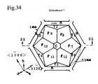
- Fig.17 shows a perspective CL view of a part of a GaN mirror wafer.
- Outlines of equilateral hexagons are a network composed of the defect accumulating regions H. Inner parts enclosed by the network are low defect density single crystal regions Z. C-plane growth regions are seen at the centers of the low defect density single crystal regions Z. In some hexagons, there is no C-plane growth regions Y.
- the dislocation density is measured by heating a mixture of phosphoric acid (H 3 PO 4 ) and sulfuric acid (H 2 SO 4 ) at a temperature of 240°C to 280°C, dipping a GaN wafer, disclosing etch pits (EP) at the points of the dislocations on the surface of the GaN wafer, observing the GaN wafer by a Nomarski interference microscope, counting the number of etch pits emerging in a definite sampling area and calculating an etch pit density (EPD) in a unit area.
- H 3 PO 4 phosphoric acid
- sulfuric acid H 2 SO 4
- AlGaInN-type LEDs are fabricated on the processed GaN wafer by an MOCVD method.
- LED chips are separated by dipping the GaN wafer into a sodium hydroxide (NaOH: higher than one normality; > 1N), corroding only the defect accumulating regions H which form a network consisting of connected closed loops, and separating the LEDs which consist of a low defect density single crystal region Z and a C-plane growth region Y from each other.
- Inhomogeneity allows the etching to corrode only the network defect accumulating regions H and divide a wafer into device chips.
- a cathode luminescence estimation confirms that defects do not impinge upon the active layers made by the MOCVD method.
- KOH potassium hydroxide
- dry-etching is also applicable to the chip-separation of the processed GaN wafer in addition to wet-etching.
- the optimum temperature for dry-etching turns out to be 700°C to 900°C.
- the dry-etching temperature is lower than an optimum epitaxial growth temperature of 1050°C. It is a favorable fact.
- the present invention differs from 3 in the shape of the defect accumulating regions H.
- the present invention endows the defect accumulating regions H with two dimensional polygon shape for forming a network of H.
- the polygon network H reduces C-plane growth regions Y.
- the polygon-repeating network defect accumulating region H enables the present invention to reduce dislocation density far lower than the parallel defect accumulating regions H in the stripe facet method 3. The reason is described.
- a C-plane growth region Y is a region which has grown with maintaining a C-plane surface without facets. Even when facets are maintained in the neighboring Zs, the C-plane growth regions are immune from the function of facets of bending dislocations.
- the stripe facet method of 3 can reduce C-plane growth regions Y by controlling growing conditions but cannot fully remove C-plane regions Y.
- C-plane growth regions Y having a (0001) plane would appear on the tops of facets for reducing free energy. Dislocations inherent in C-plane growth regions Y are transferred to neighboring low dislocation density single crystal regions Z. Linear C-plane growth regions Y accompany the stripe mask pattern growth method making linear parallel one-dimensional defect accumulating regions H and being proposed by 3 Japanese Patent Laying Open No.2003-183100 .
- the C-plane growth regions Y restrict the decrement of dislocations in the low dislocation density single crystal regions Z. EPD does not decrease below 1 ⁇ 10 6 cm -2 by the strip mask facet growth method.
- the present invention arranges defect accumulating regions H to form a closed loop, preferably to form polygons, in two dimensions.
- the area of the C-plane growth regions is reduced in comparison with parallel stripe defect accumulating regions.
- the closed loop defect accumulating regions H can reduce the dislocation density of single crystal regions Z to a tenth (1/10) of the dislocation density of single crystal regions sandwiched by linear parallel Hs.
- the present invention enables the single crystal regions Z to reduce the dislocation density (EPD) to 1 ⁇ 10 5 cm -2 .
- a more favorable condition allows single crystal regions Z to decrease EPD to 1 ⁇ 10 4 cm -2 .
- the unit shape of the closed loop for a network mask shall be a circle, an ellipse or a polygon.
- a polygon unit shape is preferable to a circle or an ellipse.
- Polygon masks allow growing nitride crystals to make symmetry facets, which have a function of eliminating dislocations, in accordance with the symmetry of undersubstrates.
- a polygonal mask allows a hexagonal (0001) undersubstrate to make distinct facet hills of regular triangles, lozenges, trapezoids or hexagons. The facets reveal a strong dislocation reduction effect.
- Vapor phase growth is suppressed on the regions to which material gases cannot attain.
- the facets appearing in vapor phase growth have inclination angles of 40 degrees to 60 degrees.
- the depth of grooves is determined by the pitch of the stripe mask pattern. For example, when the mask takes the maximum 2 mm pitch, the peak-valley depth is about 1mm for a 45 degree inclination angle. Hills and valleys align in parallel to one direction. Material gases can be neither uniformly spread nor uniformly removed at the center of the wafer. Non-uniform gas supply/removal induced by deep parallel grooves gives bad conditions to the stripe facet growth method.
- the present invention arranges closed loop masks, in particular, polygon masks with high symmetry.
- the maximum height of facets may be as high as the stripe facet growth method.
- High symmetry ensures radial-extending gas supply/removal.
- symmetric facets maintain uniform gas distribution in wide area.
- the present invention can make uniform large-sized wafers which are wider than 20 cm 2 . Occurrence of uniform growth on the whole surface is confirmed on a sample with facets of a 5mm width and about 2.5 mm height.
- the large-sized (wider than 20 cm 2 ) nitride semiconductor wafer of low defect density (minimum EPD ⁇ 1 ⁇ 10 4 cm -2 ) produced by the present invention has a wide scope of applications of making the following devices with high quality.
- LEDs and LDs Light emitting devices
- electronic devices rectifier, bipolar transistor, field effect transistor(FET), high electron mobility transistor (HEMT), and so on
- semiconductor sensors thermometer, pressure sensor, radiation sensor, visible-ultraviolet light detector, and so on
- surface acoustic wave devices SAW
- acceleration sensor MEMS parts, piezoelectric oscillator, resonator, piezoelectric actuator, and so on.
- the laser diodes (LDs) fabricated on the nitride substrates prepared by the present invention have a lifetime tens to hundreds of times as long as the lifetime of conventional on-sapphire LDs with 1 ⁇ 10 7 cm -2 EPDs in the case of large current injection of 1 ⁇ 10 3 to 1 ⁇ 10 5 A/cm 2 .
- Degeneration of nitride semiconductor light emitting devices is caused by;
- the present invention succeeds in making long lifetime devices by providing makers with very low defect density nitride substrates, suppressing substrate-originating threading dislocations from spreading into active layers of devices and preventing impurities from diffusing via defects.
- the present invention enables the devices to heighten allowable voltages of the devices, because EPDs of the substrates made by the present invention are lower than 1 ⁇ 10 7 cm -2 of conventional on-sapphire devices
- the present invention which can make substrates immune from leakpaths, enables makers to produce high sensitive sensors on low defect nitride substrates.
- a sapphire wafer having a thin GaN film of a 2 to 5 ⁇ m thickness MOCVD-grown thereupon is prepared as an undersubstrate.
- This GaN/sapphire wafer is called a sapphire template.
- Sputtering makes a 100nm thick SiO 2 film on the sapphire template.
- Conventional photolithography and etching make a SiO 2 mask pattern on the sapphire undersubstrate.
- the layer structure is SiO 2 /GaN/Sapphire from top to bottom.
- Figs.11 to 15 demonstrate units of the mask patterns. Although these figures show only one unit pattern, the masks are composed of repetitions of a unit pattern of the same shape and the same size aligning crosswise and lengthwise.
- Fig.111 is a unit pattern of an equilateral triangle. The figure shows only a unit pattern. In fact, equivalent equilateral triangle patterns are repeated lengthwise and crosswise. One side of the unit pattern triangle is parallel to a ⁇ 10-10> direction. GaN is a hexagonal system crystal. There are three equivalent directions meeting at 120 degrees. Thus all the sides of the triangle of the unit pattern are parallel to ⁇ 10-10> directions. Square-bracketed Solution is an individual representation of directions. Key-bracketed ⁇ ...> is a collective representation of directions. Collective direction ⁇ 10-1-0> includes three different individual directions [10-10], [0-110], and [-1100]. All the collective representations ⁇ 10-10>, ⁇ 0-110> and ⁇ 0-110> are equivalent and denote the same three directions above.
- GaN When GaN is grown on a sapphire C-plane undersubstrate, the GaN grows with a C-plane as a top. But GaN crystal axes twist by 90 degrees from the sapphire axes around the c-axis. GaN[10-10] direction is parallel to sapphire[11-20] direction. Figs.11-15 denote the directions of unit patterns in GaN-based directions.
- the length of the equilateral triangle unit pattern is denoted by H.
- the breadth of the unit pattern is denoted by W.
- the width of the masked parts ⁇ is denoted by T.
- the part of a width T above the SiO 2 mask is the marked parts ⁇ .
- Equilateral triangle parts enclosed by the mask are exposed parts ⁇ on which the undersubstrate reveals.
- Unit patterns A-E are all equilateral triangles but five different unit patterns of different sizes are formed on the sapphire template undersubstrates. Patterns have the following values of W, H and T.
- GaN crystals are grown on the sapphire templates covered with the patterns.A-E masks. On-mask grown GaN samples of Patterns A-E are called Samples A-E.
- the covered part ⁇ induces a defect accumulating region H thereupon.
- Low defect density single crystal regions Z are grown mainly on the exposed parts ⁇ .
- narrow C-plane growth regions appear at the centers of the exposed parts ⁇ . It is examined whether the defect accumulating region H is orientation-inversion single crystal, polycrystal or unborn (extinguished).
- Etch pit density (EPD) is counted at the centers or at peripheries of ⁇ for all samples.
- the EPDs and the properties of H are listed on Table 1. Individual explanation will follow the explanation of the crystal growth and EPD examination.
- Pattern F of mask is repetitions of a square unit pattern as shown in Fig.12.
- H and W are a length and breadth of the unit pattern, which extend in directions ⁇ 10-10>.
- a set of sides of the square is parallel to ⁇ 10-10> direction.
- Another set of sides is parallel to ⁇ 11-20> direction.
- a defect accumulating region H is produced on the mask of T. Squares of 0.9mm ⁇ 0.9mm enclosed by the network mask are exposed parts ⁇ . Low defect density single crystal regions Z are born on ⁇ . Sometimes C-plane growth regions Y are produced at the centers of ⁇ .
- Pattern G of mask is repetitions of a square unit pattern as shown in Fig.13.
- the unit pattern is a lozenge of a corner of 90 degrees, namely a square. Sides of the square are neither parallel to ⁇ 10-10> nor ⁇ 11-20>. A set of sides inclines at 45 degrees to ⁇ 10-10> and ⁇ 11-20>. Another set of sides is parallel to ⁇ 11-20> direction. Sizes of a unit pattern are W(breadth) H(length) T(mask width) Pattern G 1 mm 1 mm 0.05 mm
- a defect accumulating region H is produced on the mask of T.
- Outer square sizes of Y is 0.707mm ⁇ 0.707mm.
- Inner square sizes of ⁇ is 0.697mm ⁇ 0.697mm.
- Squares of 0.697mm ⁇ 0.697mm enclosed by the network mask are exposed parts ⁇ .
- Low defect density single crystal regions Z are born on ⁇ .
- C-plane growth regions are produced at centers of ⁇ .
- Patterns H and I of mask are repetitions of regular hexagon unit patterns as shown in Fig.14. Since the unit pattern is a regular hexagon, the size can be represented by a length of a side. Sizes are otherwise defined. H is a diameter of the hexagon. W is a distance between parallel sides. ⁇ is a mask width. Sizes of a unit pattern are W(breadth) H(length) T(mask width) Pattern H 0.1 mm 0.09 mm 0.05 mm Pattern I 2 mm 2.3 mm 0.05 mm
- Patterns H and I are regular hexagons. Pattern I is about twenty times as large as Pattern H. [5. Patterns J (Repetitions of elongated hexagon unit pattern; Fig.15)]
- Pattern J of mask is repetitions of an equiangle, elongated hexagon unit pattern as shown in Fig. 15.
- the unit pattern is an equiangle, elongate hexagon having corner angles of 120 degrees.
- Four sides are short. Two parallel sides are long. The longer sides are parallel to ⁇ 10-10> directions.
- H is the longest diameter.
- W is the shortest diameter. Sizes of a unit pattern are W(breadth) H(length) T(mask width) Pattern J 0.4 mm 20 mm 0.05 mm
- GaN crystals are grown on undersubstrates in vapor phase by an MOCVD method or HVPE method.
- GaN growth is mainly relied upon the HVPE method.
- An HVPE apparatus is composed of a tall hot-wall type furnace, a Ga-boat placed at an upper space and a resistor-heater susceptor placed at a lower space.
- a material gas of H 2 + HCl and another material gas of H 2 + NH 3 are supplied to the furnace via top inlets.
- Mask-covering undersubstrates SiO 2 /GaN/sapphire
- the susceptor is heated up to a temperature higher than 1,000°C.
- Ga Metal gallium (Ga) in the Ga-boat is heated to a Ga melt at a temperature higher than 800°C.
- Supply with H 2 +HCl gas to the Ga-melt makes GaCl(gallium chloride) vapor.
- GaCl vapor flows downward and comes to contact with the heated undersubstrate.
- Supply with H 2 +NH 3 gas to GaCl produces GaN.
- GaN falls on the undersubstrate.
- a GaN film is deposited on the undersubstrate.
- HCl partial pressure 0.02 atm (2kPa)
- GaN crystals are grown to about a 5mm thickness of a GaN ingot.
- GaN wafers are made by slicing the GaN ingot.
- GaN wafers prepared by slicing GaN ingots grown on mask Patterns A to J are called Samples A to J. Names of samples coincide with the names of patterns.
- EPD etch pit density
- the EPD shall be obtained by counting the number of etch pits appearing on a crystal surface by observing via a microscope.
- Mirror-polished wafers have no etch pits. Etching is required for revealing etch pits.
- a mixture of phosphoric acid (H 3 PO 4 ) and sulfuric acid (H 2 SO 4 ) is heated at 240°C to 280°C.
- Samples of GaN/undersubstrate are dipped into the heated H 3 PO 4 /H 2 SO 4 .
- Etch pits are revealed at dislocations on the GaN surfaces.
- Etch pit density (EPD) is obtained by counting the number of etch pits appearing in a definite area and dividing the etch pit number by the area. Embodiments count etch pits in a square of 0.1mm ⁇ 0.1mm by a Nomarski differential microscope.
- the lower limit of countable EPD by the method is 10000/cm 2 (10 4 cm -2 ).
- the upper limit of countable EPD by the method is 100000000/cm 2 (10 8 cm -2 ).
- Table 1 denotes sample symbols A-W, mask shapes, mask sizes, and EPDs at the centers and peripheries measured at discrete growth thicknesses (0.1mm, 0.5mm, 1mm, 2mm and 5mm).
- An undersubstrate is a sapphire plate templated with a 2 ⁇ m thick GaN film.
- GaN-templated sapphire undersubstrate is commonly used for Samples A-J.
- Pattern A mask (SiO 2 ) of an equilateral triangle network is formed on a 2 ⁇ m (0.002mm) GaN-templated sapphire undersubstrate (Fig.11).
- the HVPE method features high speed growth.
- the defect accumulating regions H are orientation-inversion layers (orientation is inverse to other regions Z and Y).
- EPDs are 1 ⁇ 10 7 cm -2 at the center and 1 ⁇ 10 6 cm -2 at the periphery of the exposed part II (Z+Y).
- the dislocation reduction effect on ⁇ is caused by the defect accumulating regions H on T.
- Pattern B mask (SiO 2 ) of an equilateral triangle network is formed on a 2 ⁇ m GaN-templated sapphire undersubstrate (Fig.11). GaN is grown on a Pattern B formed on the GaN-templated sapphire undersubstrate by the HVPE method. Defect accumulation regions H appear on T.
- the defect accumulating regions H are orientation-inversion layers. EPDs are 1 ⁇ 10 5 cm -2 at the center and 3 ⁇ 10 7 cm -2 at the periphery of the exposed part ⁇ (Z+Y). The dislocation reduction effect by the defect accumulating regions H is effective, in particular, at the centers on ⁇ .
- the defect accumulating regions H are orientation-inversion layers. EPDs are 1 ⁇ 10 6 cm -2 at the center and 3 ⁇ 10 7 cm -2 at the periphery of the exposed part ⁇ (Z+Y). The dislocation reduction effect by the defect accumulating regions H is effective, in particular, at the centers on ⁇ .
- the defect accumulating regions H are still orientation-inversion layers. EPDs decrease to 1 ⁇ 10 5 cm -2 at the center and 1 ⁇ 10 7 cm -2 at the periphery of ⁇ . Dislocations on ⁇ are further decreased. The defect accumulating regions H being orientation-inversion layers are effective in reducing dislocations.
- the defect accumulating regions H survive and are still orientation-inversion layers. EPDs further decrease to 1 ⁇ 10 4 cm -2 at the center and 1 ⁇ 10 6 cm -2 at the periphery of ⁇ . Polarity-inversion defect accumulating regions H powerfully decreases dislocations on ⁇ . 1 ⁇ 10 4 cm -2 of EPD, which has been unattainable low dislocation density, has been first realized by the present invention.
- defect accumulating regions H When the thickness of a GaN film is 5 mm, defect accumulating regions H partially die away and partially survive. EPDs increase to 5 ⁇ 10 5 cm -2 at the center and 1 ⁇ 10 7 cm -2 at the periphery of II. Half-extinction of the defect accumulating regions H increases dislocations on ⁇ .
- the defect accumulating regions H are orientation-inversion layers.
- EPDs are 5 ⁇ 10 6 cm -2 at the center and 3 ⁇ 10 7 cm -2 at the periphery of the exposed part ⁇ .
- the defect accumulating regions H are still orientation-inversion layers. EPDs decrease to 2 ⁇ 10 6 cm -2 at the center and 6 ⁇ 10 6 cm -2 at the periphery of ⁇ . Dislocations on ⁇ are further decreased owing to the orientation-inversion defect accumulating regions H.
- the defect accumulating regions H survive and are still orientation-inversion layers. EPDs further decrease to 5 ⁇ 10 5 cm -2 at the center and 1 ⁇ 10 7 cm -2 at the periphery of ⁇ . The surviving defect accumulating regions H powerfully decrease dislocations on ⁇ .
- defect accumulating regions H partially die away and partially survive. EPDs increase to 5 ⁇ 10 4 cm -2 at the center and 5 ⁇ 10 6 cm -2 at the periphery of ⁇ . The defect accumulating regions H still decrease dislocations on ⁇ .
- Comparison of Sample C with Sample D teaches us that a larger network pattern delays occurrence of the dislocation reduction effect later but prolongs the dislocation reduction effect against an increasing thickness.
- a wider network mask retards growth of facets from sweeping dislocations out of the exposed parts ⁇ to the mask T.
- large-size of the unit patterns endows defect accumulating regions H with a sufficient width and prolongs the life of the defect accumulating regions H against the increment of GaN film. Enlargement of the network patterns is effective for making thick, low dislocation density GaN crystals.
- the defect accumulating regions H are polycrystalline layers. EPDs are 5 ⁇ 10 6 cm -2 at the center and 3 ⁇ 10 7 cm -2 at the periphery of the exposed part ⁇ (Z+Y). With regard to the dislocation reduction effect by the defect accumulating regions H, polycrystalline Hs are as effective as orientation-inversion Hs.
- the defect accumulating regions H are polycrystalline layers. EPDs decrease to 2 ⁇ 10 6 cm -2 at the center and 1 ⁇ 10 7 cm -2 at the periphery of II. Dislocations on II are further decreased.
- the defect accumulating regions H are still polycrystals. EPDs are 5 ⁇ 10 5 cm -2 at the center and 1 ⁇ 10 7 cm -2 at the periphery of ⁇ . Polycrystalline defect accumulating regions H decrease dislocations on ⁇ .
- EPDs decrease to 1 ⁇ 10 5 cm -2 at the center and 4 ⁇ 10 7 cm -2 at the periphery of ⁇ .
- the defect accumulating regions H keep the dislocation decrement effect.
- EPDs are less than 10 6 cm -2 .
- EPDs at the centers of ⁇ decrease to 10 5 cm -2 to 10 4 cm -2 .
- Pattern F mask (SiO 2 ) of a square network is formed on a GaN-templated sapphire undersubstrate (Fig.12). Sides of the basic square are parallel to ⁇ 10-10> direction and ⁇ 11-20> direction as shown in Fig. 12.
- a GaN film is grown on the network masked undersubstrate by the HVPE method.
- the defect accumulating regions H are partially polarity-inversion crystals and partially vanished till a 1mm film thickness. When the film thickness exceeds 2mm, the defect accumulating regions H disappear. The defect decreasing effect is also extinguished. Then the dislocations increase with an increment of the film thickness.
- the defect accumulating regions H parallel to ⁇ 10-10> become orientation-inversion layers and the defect accumulating regions H parallel to ⁇ 11-20> disappear.
- EPDs are 2 ⁇ 10 6 cm -2 at the center and 3 ⁇ 10 7 cm -2 at the periphery of the exposed part ⁇ .
- the dislocation reduction effect is caused by the defect accumulating regions H partially existing.
- the defect accumulating regions H parallel to ⁇ 10-10> survive as orientation-inversion layers and the defect accumulating regions H parallel to ⁇ 11-20> do not appear.
- EPDs decrease to 5 ⁇ 10 5 cm -2 at the center and 2 ⁇ 10 7 cm -2 at the periphery of the exposed part ⁇ .
- the dislocations are more reduced than the former. This is dislocation reduction effect of the surviving orientation-inversion defect accumulating regions H.
- the defect accumulating regions H extinguish. EPDs rise to 1 ⁇ 10 6 cm -2 at the center and 2 ⁇ 10 7 cm -2 at the periphery of the exposed part ⁇ . The dislocations are rather increased. This is an effect of the extinction of the defect accumulating regions H.
- Comparison of Samples C, D, E and F implies that equilateral triangles are more suitable for a basic shape of exposed parts ⁇ than squares. Even the square network is enough to reduce the EPD to less than 10 6 cm -2 at centers of ⁇ .
- Pattern F mask (SiO 2 ) of a square network is formed on a GaN-templated sapphire undersubstrate. Sides of the basic square incline at 45 degrees to ⁇ 10-10> direction and ⁇ 11-20> direction as shown in Fig.13.
- a GaN film is grown on the network masked undersubstrate by the HVPE method.
- the defect accumulating regions H are polarity-inversion crystals which are effective in reducing dislocations till a 1mm film thickness. When the film thickness exceeds 2mm, the defect accumulating regions H vanish. The defect decreasing effect is also extinguished. Then the dislocations increase with an increment of the film thickness.
- the defect accumulating regions H inclining at 45 degrees to ⁇ 10-10> and ⁇ 11-20> become orientation-inversion layers.
- EPDs are 2 ⁇ 10 6 cm -2 at the center and 4 ⁇ 10 7 cm -2 at the periphery of the exposed part ⁇ .
- the defect accumulating regions H inclining at 45 degrees to ⁇ 10-10> and ⁇ 11-20> are orientation-inversion layers.
- EPDs decrease to 1 ⁇ 10 5 cm -2 at the center and 1 ⁇ 10 7 cm -2 at the periphery of the exposed part ⁇ .
- the dislocations are reduced. This is dislocation reduction effect of the orientation-inversion defect accumulating regions H.
- the defect accumulating regions H extinguish. EPDs rise to 5 ⁇ 10 5 cm -2 at the center and 1 ⁇ 10 7 cm -2 at the periphery of the exposed part ⁇ . The dislocations are slightly increased. This is an effect of the extinction of the defect accumulating regions H.
- Comparison of Samples F and G teaches us that the square mask with sides not parallel to ⁇ 10-10> and ⁇ 11-20> is preferable to the square mask with sides parallel with ⁇ 10-10> and ⁇ 11-20> for decreasing dislocations and prolonging the life of defect accumulating regions H.
- ⁇ 11-20> direction extending defect accumulating regions in particular, have a stronger tendency to disappear. The reason is not clear now.
- Pattern H mask (SiO 2 ) of a hexagon network is formed on a GaN-templated sapphire undersubstrate (Fig.14).
- a GaN film is grown on the network masked undersubstrate by the HVPE method.
- the defect accumulating regions H are polarity-inversion crystals which are effective in reducing dislocations till a 1mm film thickness. When the film thickness exceeds 2mm, the defect accumulating regions H vanish. Then the dislocations increase with an increment of the film thickness.
- the defect accumulating regions H are orientation-inversion layers.
- EPDs are 8 ⁇ 10 4 cm -2 at the center, which is rarely low density for 0.5mm thick films, and 3 ⁇ 10 7 cm -2 at the periphery of the exposed part ⁇ .
- the defect accumulating regions H are orientation-inversion layers. EPDs decrease to 1 ⁇ 10 4 cm -2 at the center, which is distinguished low density and 5 ⁇ 10 5 cm -2 at the periphery of the exposed part ⁇ . The dislocations are moreover reduced. This is dislocation reduction effect of the orientation-inversion defect accumulating regions H.
- the defect accumulating regions H disappear. EPDs rise to 8 ⁇ 10 4 cm -2 at the center and 1 ⁇ 10 7 cm -2 at the periphery of the exposed part ⁇ . The dislocations are increased to a level similar to the 0.5mm thickness. This is an effect of the extinction of the defect accumulating regions H.
- Results of Samples C, D, E, F, G and H imply that equilateral triangles are preferable to squares, and regular hexagons are preferable to equilateral triangles as polygons building a network of masks.
- the hexagon network mask enables the HVPE grown GaN crystal to reduce dislocations down to 1 ⁇ 10 4 cm -2 .
- Pattern I mask (SiO 2 ) of a hexagon network is formed on a GaN-templated sapphire undersubstrate (Fig.14).
- a GaN film is grown on the network masked undersubstrate by the HVPE method.
- the defect accumulating regions H are polarity-inversion crystals which are effective in reducing dislocations till a 1mm film thickness. When the film thickness exceeds 2mm, the defect accumulating regions disappear. Then the dislocations increase with an increment of the film thickness.
- the defect accumulating regions H are orientation-inversion layers.
- EPDs are 5 ⁇ 10 6 cm -2 at the center and 4 ⁇ 10 7 cm -2 at the periphery of the exposed part ⁇ .
- the defect accumulating regions H are orientation-inversion layers. EPDs decrease to 2 ⁇ 10 6 cm -2 at the center and 6 ⁇ 10 6 cm -2 at the periphery of the exposed part ⁇ . The dislocations are reduced. This is dislocation reduction effect of the orientation-inversion defect accumulating regions H.
- Pattern J mask (SiO 2 ) of an elongated hexagon network is formed on a GaN-templated sapphire undersubstrate (Fig.15).
- a GaN film is grown on the network masked undersubstrate by the HVPE method.
- the defect accumulating regions H are polarity-inversion crystals which are effective in reducing dislocations till a 5mm film thickness.
- the defect accumulating regions H are orientation-inversion layers.
- EPDs are 5 ⁇ 10 6 cm -2 at the center and 2 ⁇ 10 7 cm -2 at the periphery of ⁇ .
- the defect accumulating regions H are orientation-inversion layers. EPDs decrease to 1 ⁇ 10 6 cm -2 at the center and 5 ⁇ 10 6 cm -2 at the periphery of ⁇ . The dislocations are reduced. This is dislocation reduction effect of the orientation-inversion defect accumulating regions H.
- the defect accumulating regions H are orientation-inversion. EPDs rise to 8 ⁇ 10 5 cm -2 at the center and 3 ⁇ 10 6 cm -2 at the periphery of the exposed part ⁇ . Dislocations decrease due to the defect accumulating regions H.
- the defect accumulating regions H are orientation-inversion. EPDs decrease to 7 ⁇ 10 5 cm -2 at the center and 3 ⁇ 10 6 cm -2 at the periphery of the exposed part ⁇ . Defect accumulating regions H decrease dislocations.
- a narrower mask width T makes a narrower defect accumulating region H.
- the progress of GaN growth slenderizes defect accumulating regions H.
- a further GaN growth extinguishes defect accumulating regions H.
- Fluctuation from ⁇ 10-10> direction within ⁇ 15 degrees allows masks to form defect accumulating regions H as planar defects.
- Embodiment 2 makes use of undersubstrates made of GaAs(111)A (Sample K), Si (Sample L), SiC (Sample M) and sapphire (Sample N).
- Network masks are made on a variety of undersubstrates. GaN films are grown on the network masked undersubstrates. Properties of the defect accumulating regions H yielded on the masked undersubstrates are examined.
- SiO 2 mask patterns there are four kinds of SiO 2 mask patterns, K, L, M, and N. Every SiO 2 mask pattern is produced by piling a SiO 2 layer with a thickness of 100 nm on an undersubstrate, and making a pattern by ordinary photolithography and etching. All of the mask patterns are the same regular hexagon. W(mm) H(mm) T(mm) Pattern K (GaAs undersubstrate) 1 1.2 0.05 Pattern L (Si undersubstrate) 1 1.2 0.05 Pattern M (6h-SiC undersubstrate) 1 1.2 0.05 Pattern N (sapphire undersubstrate) 1 1.2 0.05
- a GaN film is grown on each undersubstrate by the HVPE method.
- the GaN film is composed of two layers, one is a layer piled at a low temperature (buffer layer) and the other is a layer piled at a high temperature (epitaxial layer).
- All the undersubstrates can make defect accumulating regions H. It is confirmed that GaAs(111)A, sapphire and SiC undersubstrates enable the masks to make the defect accumulating regions H having planar defects on the mask covered parts T.
- the Si mask fails to make the defect accumulating regions H having planar defects. Si reacts with Ga in GaAs. The reaction impedes the Si mask from making clear growth boundaries.
- Fig.16 demonstrates a gallium nitride crystal grown on the GaAs(111)A mask.
- Defect accumulating regions H are made on the hexagon network mask T.
- Hexagon cone GaN crystals are grown on ⁇ enclosed by the defect accumulating regions H.
- Small horizontal flats remain on the tops of the hexagon cones.
- Inclination walls of the hexagon cones are facets.
- the parts covered with the facets are low defect density single crystal regions Z.
- the flat tops are C-plane growth regions Y.
- the inclination angles are predetermined.
- Hexagon cones occupying the exposed parts ⁇ have high peaks.
- the rugged crystal shall be sliced at heights below the surface of the defect accumulating regions H. As-cut wafers are obtained by slicing the rugged crystal in the horizontal direction below the surface of the network defect accumulating regions H. Smooth-surfaced mirror wafers are also made by polishing both surfaces.
- Fig. 17 is a slanting view of a mirror polished wafer.
- a plurality of regular hexagonal low defect density single crystal regions Z align lengthwise and crosswise.
- Zs are single crystals with low dislocation density and high quality.
- a network defect accumulating region H fills the gap of the low dislocation density single crystal regions Z.
- C-plane growth regions Y exist at the centers of Zs. The C-plane regions take a variety of shapes and sizes. Human eyesight cannot observe such an inner structure. Cathode luminescence (CL) clarified the inner structure.
- Samples K, L, M and N employ different undersubstrates of GaAs, Si, 6h-SiC and sapphire respectively.
- Pattern K mask (SiO 2 ) of a regular hexagon network is formed on a GaAs(111)A-plane undersubstrate (Fig.14).
- A-plane denotes a Ga-plane, on which Ga atoms appear overall.
- a GaN film is grown on the network masked undersubstrate by the HVPE method.
- the defect accumulating regions H are polarity-inversion crystals which are effective in reducing dislocations till a 1mm film thickness. As the film thickness exceeds 1mm, the defect accumulating regions H vanish. After the extinction, the effect of reducing dislocations is maintained at the centers of ⁇ .
- the defect accumulating regions H are orientation-inversion layers.
- EPDs are 2 ⁇ 10 6 cm -2 at the center and 3 ⁇ 10 7 cm -2 at the periphery of ⁇ . Dislocation reduction is caused by the orientation-inversion defect accumulating regions H.
- the defect accumulating regions H are orientation-inversion layers. EPDs decrease to 1 ⁇ 10 5 cm -2 at the center and 1 ⁇ 10 6 cm -2 at the periphery of ⁇ . The dislocations are further reduced by the defect accumulating regions H.
- EPDs are 1 ⁇ 10 4 cm -2 at the center and 1 ⁇ 10 7 cm -2 at the periphery of ⁇ .
- the GaN growth is ended at a GaN thickness of 2mm, because the defect accumulating regions H vanish.
- Comparison of Sample K with Sample I suggests that GaAs undersubstrates are more effective than GaN/sapphire undersubstrates in reducing dislocations (EPDs).
- Samples L employs a Si undersubstrate.
- a GaN film is grown on the network masked undersubstrate by the HVPE method. No defect accumulating region H appears on the covered parts T from the beginning.
- Sample L has an weak effect of reducing dislocations due to facets.
- Si is unfavorable to undersubstrates, because Si undersubstrates cannot generate defect accumulating regions from the beginning.
- EPDs are 3 ⁇ 10 5 cm -2 at the center and 3 ⁇ 10 6 cm -2 at the periphery of ⁇ .
- EPDs are 3 ⁇ 10 4 cm -2 at the center and 2 ⁇ 10 7 cm -2 at the periphery of ⁇ .
- Samples M employs a 6h-SiC undersubstrate.
- "6h-" means hexagonal system.
- a GaN film is grown on the network masked undersubstrate by the HVPE method. Defect accumulating regions H of orientation-inversion appear on the covered parts T from the beginning and survive till a 1mm thickness but disappear at a 2mm thickness. Dislocations at centers on exposed parts ⁇ keep reducing till a 2mm thickness due to the delayed effect of the defect accumulating regions H. It is confirmed that 6h-SiC undersubstrate enables the mask to produce the defect accumulating regions H.
- SiC has an intermediate undersubstrate-preference less than GaAs but more than Si.
- defect accumulating regions H are orientation-inversion layers yielded on the mask part T EPDs are 2 ⁇ 10 6 cm -2 at the center and 4 ⁇ 10 7 cm -2 at the periphery of ⁇ . Dislocation reduction is caused by the orieritation-inversion defect accumulating regions H.
- EPDs are 2 ⁇ 10 5 cm -2 at the center and 2 ⁇ 10 6 cm -2 at the periphery of ⁇ .
- EPDs are 2 ⁇ 10 4 cm -2 at the center and 1 ⁇ 10 7 cm -2 at the periphery of ⁇ .
- Samples N employs a sapphire ( ⁇ -Al 2 O 3 ) undersubstrate.
- Samples A to J employ GaN templated sapphire (GaN/sapphire) as undersubstrates.
- Sample N adopts a pure sapphire (0001) undersubstrate.
- a GaN film is grown on the network masked undersubstrate by the HVPE method. Defect accumulating regions H appear on the covered parts T from the beginning and survive till a 1mm thickness but disappear at a 2mm thickness.
- Dislocations at the centers on exposed parts II keep reducing till a 2mm thickness due to the delayed effect of the defect accumulating regions H. It is confirmed that sapphire undersubstrate enables the mask to produce the defect accumulating regions H. Sapphire seems to have an undersubstrate-preference better than GaAs, SiC and Si.
- defect accumulating regions H are orientation-inversion layers yielded on the mask part Y.
- EPDs are 1 ⁇ 10 6 cm -2 at the center and 2 ⁇ 10 7 cm -2 at the periphery of ⁇ . Dislocation reduction is caused by the orientation-inversion defect accumulating regions H.
- EPDs are 1 ⁇ 10 5 cm -2 at the center and 1 ⁇ 10 6 cm -2 at the periphery of ⁇ .
- EPDs are 2 ⁇ 10 4 cm -2 at the center and 1 ⁇ 10 7 cm -2 at the periphery of ⁇ .
- Comparison of Samples K to N indicates that the degree of undersubstrate-preference should be an order of sapphire, GaAs, SiC and Si.
- Crystallographic properties of Sample K wafer are examined by the X-ray diffraction method.
- Spectrics X' pert-MRD is an X-ray diffraction apparatus.
- An effective area of X-rays irradiated on the sample is determined to be less than 0.25mm 2 by adjusting a slit aperture.
- X-ray diffraction power at (004) planes is measured.
- (004) is a three index expression.
- An equivalent four index expression is (0004).
- Fig.18 exhibits the angular distribution of the X-ray diffraction.
- the ordinate is diffracted ray counts (counts/second).
- the FWHM full width at half maximum
- the narrow FWHM means a good crystal lattice structure.
- Sample K is a GaN on GaAs undersubstrate. It is confirmed that other samples grown on SiC or sapphire have a similar good lattice structure by the X-ray diffraction.
- the wafer of Sample K is input into an MOCVD apparatus. LEDs are produced on the sample K wafer by supplying organic materials and ammonia to the wafer.
- Fig.19 denotes the structure of the LED.
- a 5 ⁇ m n-GaN buffer layer, a 150nm n-Al 0.15 Ga 0.85 N layer, a 50nm n-In 0.06 Ga 0.94 N layer, a 150nm p-Al 0.15 Ga 0.85 N layer and a 500nm p-GaN layer are grown on the GaN substrate.
- a Ni/Au p-electrode is deposited on the top.
- a Ti/Al n-electrode is formed on the bottom. After the formation of the electrodes, the bottom surface is protected by covering with wax.
- Four hour selective etching in a hot KOH solution (1N; 100°C) eliminates only the defect accumulating regions H which form a hexagon network.
- Hexagon LED chips which are denoted by "LED 1" are produced from (Embodiment 2) Sample K.
- LED 1 (Embodiment 2) and LED 2(Comparison) are driven by supplying current on the same condition. Emission intensity of LED 1 is about 1.2 times as strong as LED 2 at 20mA current supply.
- a lifetime test on the condition of 100mA current supply confirms that LED 1 has a lifetime more than ten times as long as the lifetime of LED 2.
- the long lifetime proves high quality and low defect density of the substrates made by the present invention.
- Samples O-R change materials of masks.
- SiO 2 (Sample O), Si 3 N 4 (Sample P), Pt(Sample Q) and W (Sample R) mask are used. All the masks of SiO 2 , Si 3 N 4 , Pt and W have a common 100nm thickness.
- Sample R (W mask) 1 1.2 0.05
- Thin buffer layers are made at a low temperature on the masked undersubstrates.
- Thick epitaxial layers are made at a high temperature on the buffer layers.
- the SiO 2 mask enables Sample O to make defect accumulating regions H including plane defects on the SiO 2 mask on GaAs. But the Si 3 N 4 mask (Sample P) is incapable of making defect accumulating regions H including plane defects on the Si 3 N 4 mask on GaAs.
- the Pt mask (Sample Q) and the W mask (Sample R) can make defect accumulating regions H thereon. But the defect accumulating regions H are polycrystals.
- the SiO 2 mask is the best for making definite defect accumulating regions H of orientation-inversion single crystals thereon.
- Embodiment 3 which includes Samples O, P, Q and R, employs a GaAs(111)A-plane single crystal undersubstrate in common but produces masks with different materials.
- Mask materials are SiO 2 (silicon dioxide), Si 3 N 4 (silicon nitride), Pt (platinum) and W (tungsten) for Samples O, P, Q and R respectively.
- a GaN film is grown on the network masked undersubstrate by the HVPE method. Defect accumulating regions H of orientation-inversion appear on the covered parts T from the beginning and survive till a 1mm thickness but disappear at a 2mm thickness. Delayed effect of the defect accumulating regions H keeps reducing EPDs on the centers of ⁇ .
- defect accumulating regions H are orientation-inversion layers.
- EPDs are 2 ⁇ 10 6 cm -2 at the center and 3 ⁇ 10 7 cm -2 at the periphery of II. Dislocation reduction is caused by the orientation-inversion defect accumulating regions H.
- defect accumulating regions H are orientation-inversion.
- EPDs are 1 ⁇ 10 5 cm -2 at the center and 1 ⁇ 10 6 cm -2 at the periphery of ⁇ . The EPD reduction is caused by the defect accumulating regions H.
- a GaN film is grown on the network masked undersubstrate by the HVPE method. No defect accumulating region H appears from the beginning. Facet hills ⁇ are made on ⁇ . Facets have a function of conveying dislocations to the masked parts T.
- EPDs are 2 ⁇ 10 6 cm -2 at the center and 2 ⁇ 10 7 cm -2 at the periphery of II. Dislocation reduction is owed to the facet hills ⁇ and mask parts ⁇ .
- EPDs are 1 ⁇ 10 6 cm -2 at the center and 2 ⁇ 10 6 cm -2 at the periphery of ⁇ .
- the EPD reduction is caused by ⁇ and T.
- a GaN film is grown on the network masked undersubstrate by the HVPE method.
- Polycrystalline defect accumulating regions H appear from the beginning. Dislocations at both the center parts of ⁇ and the peripheral parts of ⁇ are decreased lower by the polycrystal defect accumulating regions H as the GaN film grows thicker.
- defect accumulating regions H are polycrystals. EPDs are 5 ⁇ 10 6 cm -2 at the center and 5 ⁇ 10 7 cm -2 at the periphery of ⁇ . Dislocation reduction is owed to the polycrystalline defect accumulating regions H.
- defect accumulating region H are polycrystalline. EPDs are 5 ⁇ 10 5 cm -2 at the center and 5 ⁇ 10 6 cm -2 at the periphery of II. The EPD reduction is caused by the polycrystalline defect accumulating regions H.
- defect accumulating regions H exist as polycrystals.
- EPDs are 2 ⁇ 10 5 cm -2 at the center and 2 ⁇ 10 6 cm -2 at the periphery of ⁇ .
- the defect accumulating regions H keep reducing EPD on the center and the periphery of ⁇ .
- the Pt mask is incapable of lowering EPDs below 2 ⁇ 10 5 cm -2 .
- Pt is competent for a mask material, since Pt maintains polycrystal defect accumulating regions H to more than a 2mm thickness.
- a GaN film is grown on the network masked undersubstrate by the HVPE method.
- Polycrystalline defect accumulating regions H appear from the beginning to a 2mm thickness of growth. Dislocations are decreased lower by the polycrystal defect accumulating regions H as the GaN film grows thicker.
- defect accumulating regions H are polycrystals. EPDs are 3 ⁇ 10 6 cm -2 at the center and 3 ⁇ 10 7 cm -2 at the periphery of ⁇ . Dislocation reduction is owed to the polycrystalline defect accumulating regions H.
- defect accumulating region H are polycrystalline. EPDs are 3 ⁇ 105cm -2 at the center and 3 ⁇ 10 6 cm -2 at the periphery of ⁇ . The EPD reduction is caused by the polycrystalline defect accumulating regions H.
- defect accumulating regions H still exist as polycrystals.
- EPDs are 2 ⁇ 10 5 cm -2 at the center and 2 ⁇ 10 6 cm -2 at the periphery of ⁇ .
- the defect accumulating regions H keep reducing EPD on both the center and the periphery of ⁇ .
- Tungsten masks are incapable of lowering EPDs below 2 ⁇ 10 5 cm -2 .
- Tungsten (W) is competent for a mask material, since tungsten maintains polycrystal defect accumulating regions H to more than a 2mm thickness.
- Pt, W or other metallic masks have a tendency of producing polycrystal defect accumulating regions H.
- Platinum (Pt) and tungsten (W) are inferior to SiO 2 in EPD decrement but superior to SiO 2 in long-term EPD reduction via longlife polycrystalline defect accumulating regions H.
- Tungsten (W) surpasses platinum (Pt) in EPD reduction.
- All the preceding embodiments aim at producing gallium nitride (GaN) substrates.
- the present invention is applicable to production of other nitride crystal substrates, for example, AIN and InN substrates with some additional contrivances.
- AlN aluminum nitride
- SiO 2 silicon dioxide
- Si 3 N 4 silicon nitride
- AIN will grow on a mask at the same speed as on an undersubstrate.
- Aluminum nitride (AlN) cannot induce facet-growth.
- a contrivance is used for AIN growth, which includes the processes of forming a mask on undersubstrate, growing GaN on the masked undersubstrate, making an inhomogeneous GaN crystal having Zs an Hs, slicing the GaN crystal into an inhomogeneous GaN wafer and assigning the inhomogeneous GaN wafer as an undersubstrate.
- Embodiment 4 selects Sample K GaN wafer prepared by Embodiment 2 which has been made by forming a SiO 2 mask on a GaAs(111)A-plane, growing a GaN buffer layer and thick GaN epitaxial layers on the masked undersubstrate by the HVPE method and slicing the GaN crystal.
- the GaN undersubstrate made by Embodiment 2 has a hexagon network defect accumulating region H, hexagon low defect density single crystal regions Z enclosed by H and C-plane growth regions Y at the centers of the hexagons.
- Samples S, T and U will be GaN, AlGaN and InGaN wafers having hexagonal structure of H+Z+Y made on Sample K.
- Sample U (GaN undersubstrate K) 1mm 1.2mm 0.05mm
- the above parameters are not mask parameters of Samples S, T and U but the mask parametesr of Sample K, which has been described.
- Samples S, T and U try to grow GaN, AlGaN and InGaN crystals by the HVPE method. Samples S, T and U have many common points in the HVPE growth. As undersubstrates, Samples S, T, U and W employ a GaN mirror wafer K prepared by cutting the GaN crystal produced by Embodiment 2 into thin as-cut wafers and polishing the as-cut wafers into GaN mirror wafers. The mirror wafer K lacks a mask. But the wafer K has a potential structure composed of hexagonal network Hs and isolated hexagon Zs and Ys. Sample S grows a GaN crystal on an unmasked, potential-structured GaN undersubstrate K. Sample T grows an AlGaN crystal on an unmasked, potential-structured GaN undersubstrate K. Sample U grows an InGaN crystal on an unmasked, potential-structured GaN undersubstrate K.
- Samples S employs the product of Sample K as an undersubstrate for making a new GaN substrate.
- the Sample K GaN/GaAs wafer is placed upon a susceptor in the HVPE furnace.
- the Ga-melt temperature is 800°C.
- the growth temperature is 1050°C.
- the HVPE apparatus supplies a Ga-melt with HCl+H 2 gas, produces gallium chloride (GaCl) gas, guides the GaCl gas to the 1050°C heated susceptor, and supplies NH 3 +H 2 gas to the susceptor. Reaction of GaCl with NH 3 synthesizes GaN.
- GaN film is grown on the GaN/GaAs (Sample K) undersubstrate.
- high temperature HVPE method Ga temperature : 800°C GaCl synthesis : ( ⁇ Ga+HCl) undersubstrate temperature : 1050°C NH 3 partial pressure : 2.5 ⁇ 10 -2 atm (2.5kPa) HCl partial pressure : 0.02 atm (2 kPa) Growth time : 30 hours
- the new GaN crystal grows with defect accumulating regions H whose positions and sizes are the same as the defect accumulating regions H on Sample K.
- New defect accumulating regions H grow on the defect accumulating regions H of the undersubstrate K.
- Hexagonal defect accumulating regions H are produced.
- New low defect density single crystal regions Z grow on the low defect density single crystal regions Z of the undersubstrate K.
- the new GaN crystal copies and transcribes the ZHY structure of the GaN undersubstrate.
- Samples T employs the product of Sample K as an undersubstrate for making a new AlGaN substrate.
- the Sample K GaN/GaAs wafer is placed upon a susceptor in the HVPE furnace.
- the Ga-melt temperature is 800°C.
- the Al-melt temperature is 500°C to 600°C.
- the growth temperature is 1050°C.
- the HVPE apparatus supplies a Ga-melt with HCl+H 2 gas, produces gallium chloride (GaCl) gas, supplies Al-melt with HCl+H 2 gas, produces aluminum chloride gas (AlCl 3 ), guides the GaCl and AlCl 3 gases to the 1050°C heated susceptor, and supplies NH 3 +H 2 gas to the susceptor. Reaction of GaCl+AlCl 3 with NH 3 synthesizes AlGaN. An AlGaN film is grown on the GaN/GaAs (Sample K) undersubstrate.
- the new AlGaN crystal grows with defect accumulating regions H whose positions and sizes are the same as the defect accumulating regions H on Sample K.
- New defect accumulating regions H grow on the defect accumulating regions H of the undersubstrate K.
- Hexagonal defect accumulating regions H are produced.
- New low defect density single crystal regions Z grow on the low defect density single crystal regions Z of the undersubstrate K.
- the new AIGaN crystal copies and transcribes the ZHY structure of the GaN undersubstrate.
- Samples U employs the product of Sample K as an undersubstrate for making a new InGaN substrate.
- the Sample K GaN/GaAs wafer is placed upon a susceptor in the HVPE furnace.
- the Ga-melt temperature is 800°C.
- the In-melt temperature is 100°C to 120°C.
- the growth temperature is 1050°C.
- the HVPE apparatus supplies a Ga-melt with HCl+H 2 gas, produces gallium chloride (GaCl) gas, supplies an In-melt with HCl+H 2 gas, produces indium chloride gas (InCl 3 ), guides the GaCl and InCl 3 gases to the 1050 ⁇ heated susceptor, and supplies NH 3 +H 2 gas to the susceptor. Reaction of GaCl+InCl 3 with NH 3 synthesizes AlGaN. An InGaN film is grown on the GaN/GaAs (Sample K) undersubstrate.
- the new InGaN crystal grows with defect accumulating regions H whose positions and sizes are the same as the defect accumulating regions H on Sample K.
- New defect accumulating regions H grow on the defect accumulating regions H of the undersubstrate K.
- Hexagonal defect accumulating regions H are produced.
- New low defect density single crystal regions Z grow on the low defect density single crystal regions Z of the undersubstrate K.
- the new InGaN crystal copies and transcribes the ZHY structure of the GaN undersubstrate.
- Non-C-plane substrates are made by cutting the GaN crystals produced by Embodiment 2 in parallel with (10-10) and (11-22) planes, making (10-10) as-cut GaN wafers and (11-22) as-cut wafers and producing (10-10) mirror wafers for Sample V and (11-22) mirror wafers for Sample W.
- Sample V is a GaN film grown on the (10-10) mirror GaN wafer. All the defect accumulating regions H vanish in the (10-10) GaN crystal. The present invention seems to be inapplicable to (10-10) orientation. (10-10) is a plane orthogonal to C-plane (0001).
- Sample V is a GaN film grown on the (11-22) mirror GaN wafer.
- Defect accumulating regions H which are polycrystals, appear on the (11-22) GaN crystal.
- the present invention is applicable to (11-22) orientation.
- (11-22) is not orthogonal to C-plane but one of facets.
- Samples S employs the product of Sample K as an undersubstrate.
- Sample S has no mask but has potential network of hexagonal Hs and Zs originating from Sample K.
- New GaN defect accumulating regions H succeed to the substrate defect accumulating regions H.
- New GaN low dislocation single crystal regions Z grow on the substrate low dislocations single crystal regions Z.
- GaN film transcribes the GaN undersubstrate (Sample K).
- the defect accumulating regions H survive till a 1mm thickness but disappear at a 2mm thickness. Defect accumulating regions H succeed to the substrate defect accumulating regions H.
- defect accumulating regions H are orientation-inversion.
- EPDs are 1 ⁇ 10 6 cm -2 at the center and 1 ⁇ 10 7 cm -2 at the periphery of ⁇ . Dislocation reduction is owed to the orientation-inversion defect accumulating regions H.
- defect accumulating regions H are polycrystalline. EPDs are 1 ⁇ 10 5 cm -2 at the center and 1 ⁇ 10 6 cm -2 at the periphery of ⁇ . The EPD reduction is caused by the defect accumulating regions H.
- defect accumulating regions H vanish. EPDs are 1 ⁇ 10 4 cm -2 at the center and 1 ⁇ 10 7 cm -2 at the periphery of ⁇ . The defect accumulating regions H keep reducing EPD on both the center and the periphery of ⁇ .
- Sample S gives a valuable hint of making use of the GaN crystal produced by the present invention as a substrate.
- GaN is grown on a GaN substrate having a potential structure of defect accumulating regions H and low defect density single crystal regions Z
- the growing GaN crystal transcribes the potential structure with fidelity.
- Defect accumulating regions H succeed to the original defect accumulating regions H.
- Low defect density single crystal regions Z follow the original low defect density single crystal regions Z.
- C-plane growth regions Y accompany the original C-plane growth regions Y. Attention should be paid to anisotropy and periodicity of the substrates made by the present invention.
- Sample T employs the product of Sample K as an undersubstrate.
- An AlGaN mixture film is grown upon the GaN undersubstrate.
- New AlGaN defect accumulating regions H succeed to the substrate defect accumulating regions H.
- New AlGaN low dislocation single crystal regions Z grow on the substrate low dislocations single crystal regions Z. Namely a newly growing AlGaN film transcribes the GaN undersubstrate (Sample K).
- the defect accumulating regions H survive till a 0.5mm thickness but disappear at a 1mm thickness.
- defect accumulating regions H are orientation-inversion.
- EPDs in AlGaN are 1 ⁇ 10 6 cm -2 at the center and 1 ⁇ 10 7 cm -2 at the periphery of ⁇ . Dislocation reduction is owed to the orientation-inversion defect accumulating regions H.
- EPDs in AlGaN are 1 ⁇ 10 5 cm -2 at the center and 1 ⁇ 10 7 cm -2 at the periphery of ⁇ .
- Sample T gives a valuable hint of making use of the AlGaN crystal produced by the present invention as a substrate.
- AlGaN is grown on a GaN substrate having a potential structure of defect accumulating regions H and low defect density single crystal regions Z
- the growing AlGaN crystal transcribes the potential structure with fidelity.
- Defect accumulating regions H succeed to the original defect accumulating regions H.
- Low defect density single crystal regions follow the original low defect density single crystal regions Z.
- C-plane growth regions Y accompany the original C-plane growth regions Y. Attention should be paid to anisotropy and periodicity of the substrates made by the present invention.
- Sample U employs the product of Sample K as an undersubstrate.
- An InGaN mixture film is grown upon the GaN undersubstrate.
- New InGaN defect accumulating regions H succeed to the substrate defect accumulating regions H.
- New InGaN low dislocation single crystal regions Z grow on the substrate low dislocations single crystal regions Z. Namely a newly growing InGaN film transcribes the GaN undersubstrate (Sample K).
- the defect accumulating regions H survive till a 1 mm thickness but disappear at a 2mm thickness.
- defect accumulating regions H are orientation-inversion.
- EPDs in InGaN are 1 ⁇ 10 6 cm -2 at the center and 1 ⁇ 10 7 cm -2 at the periphery of II. Dislocation reduction is owed to the orientation-inversion defect accumulating regions H.
- EPDs in InGaN are 5 ⁇ 10 5 cm -2 at the center and 3 ⁇ 10 7 cm -2 at the periphery of ⁇ .
- EPDs in InGaN are 2 ⁇ 10 5 cm -2 at the center and 3 ⁇ 10 7 cm -2 at the periphery of ⁇ .
- Sample U gives an important hint of making use of the GaN crystal produced by the present invention as a substrate.
- InGaN is grown on a GaN substrate having a potential structure of defect accumulating regions H and low defect density single crystal regions Z
- the growing InGaN crystal transcribes the potential structure with fidelity.
- Defect accumulating regions H succeed to the original defect accumulating regions H.
- Low defect density single crystal regions Z follow the original low defect density single crystal regions Z.
- C-plane growth regions Y accompany the original C-plane growth regions Y. Attention should be paid to anisotropy and periodicity of the substrates made by the present invention.
- Sample V employs a (10-10) plane cut GaN of Sample K as an undersubstrate.
- a GaN film is grown upon the (10-10)-cut GaN undersubstrate.
- New GaN defect accumulating regions H succeed to the substrate defect accumulating regions H. But the newly born defect accumulating regions H vanish soon.
- the dislocation decrement device is inactive.
- EPDs are 2 ⁇ 10 7 cm -2 at the center and 2 ⁇ 10 7 cm -2 at the periphery of ⁇ . Dislocations are not reduced owing to the extinction of effect accumulating regions H.
- EPDs are 1 ⁇ 10 7 cm -2 at the center and 1 ⁇ 10 7 cm -2 at the periphery of ⁇ .
- Sample W employs a (11-22) plane cut GaN of Sample K as an undersubstrate.
- a GaN film is grown upon the (11-22)-cut GaN undersubstrate.
- New GaN defect accumulating regions H succeed to the substrate defect accumulating regions H.
- the newly born defect accumulating regions H are polycrystals.
- polycrystalline defect accumulating regions H act as a dislocation decrement device.
- defect accumulating regions H are polycrystals.
- EPDs are 2 ⁇ 10 7 cm -2 at the center and 2 ⁇ 10 7 cm -2 at the periphery of ⁇ .
- defect accumulating regions H are polycrystals.
- EPDs are 1 ⁇ 10 6 cm -2 at the center and 1 ⁇ 10 7 cm -2 at the periphery of ⁇ .
- defect accumulating regions H are polycrystals. EPDs are 5 ⁇ 10 5 cm -2 at the center and 1 ⁇ 10 7 cm -2 at the periphery of ⁇ . Sample K is inherently sufficiently low EPDs. There is an additional EPD decrement effect in Sample W, which has polycrystalline defect accumulating regions H.
- the essence of the present invention is to make a low defect GaN or other nitride substrates by forming a network mask pattern composed of repetitions of a unit closed looped polygon on an undersubstrate, growing GaN or other nitrides in vapor phase on the network masked undersubstrate, gathering dislocations on the closed looped mask and producing defect accumulating regions H of the closed loops. Defect accumulating regions H accompany as-grown GaN crystals somewhere. All the examples which have been explained are still plagued with the residual defect accumulating regions H.
- An ultralow defect density crystal (theoretically 0 density) can be obtained by growing a tall wide GaN crystal on a wide masked undersubstrate and cutting a part immune from dislocations.
- Ultralow defect density single crystal GaN wafers are obtained by cutting the ultralow defect density single crystal inner contact cylindrical column into thin round wafers. Substrate wafers are shaped into round wafers for the convenience of handling in many cases. Thus circular wafers are sliced out of the ultralow defect density single crystal inner contact cylindrical column.
- Fig.35 which is a vertical sectional view of the hexagon crystal depicted in Fig.34, can be applied to any polygon mask case.
- a Ti (titanium) network mask is formed on the undersubstrate. GaN facetted-grows on an exposed part within the mask.
- a radius r of a facet is now defined as a breadth of the facet in the direction orthogonal to the contact side. The radius r can be defined to every individual facet. Since a C-plane sometimes intervenes, 2r is not necessarily equal to a distance between two neighboring masks.
- Fig.35 crystals grow upward within the radius r of a facet on an exposed part ⁇ . Dislocations accompany the vertical growth. Dotted lines designate dislocations. Dislocations prolong in the vertical direction with the growth of crystals The vertical growth continues till the crystals form a cone (facet hill) without riding over the masks.
- a conical crystal (facet hill) which is denoted by a solid line in Fig.35, is completely formed on ⁇ within the mask.
- the radius r is a horizontal distance from the center to the mask edge.
- the facet inclines at ⁇ to the horizontal plane. ⁇ is called an inclination angle.
- the present invention does not bury facets but maintains facet hills.
- directions of crystal growth change from the vertical direction to slanting directions orthogonal to the facets.
- Dislocations, which follow the growth, extend in right and left slanting directions normal to the right and left facets in Fig.35.
- Slanting dotted lines show dislocations extending outward.
- Divided dislocations come near to the spaces above the masks.
- Another set of dislocations extend from neighboring II at a reciprocal slanting angle toward the space above the mask.
- Two sets of dislocations collide and aggregate above the mask. After the collision, the aggregated dislocations extend in the vertical direction just above the masks. The regions above the masks become defect accumulating regions H.
- the dislocation ascends in the vertical direction by xtan ⁇ till the solid-line cone.
- the dislocation changes the extending direction leftward to the normal standing on the facet.
- the change of angle is ⁇ .
- the dislocation goes up slantingly toward the defect accumulating region H.
- the crossing angle of the dislocation to H is also ⁇ .
- the path length of the slanting dislocation going from the cone to H is xcosec ⁇ .
- the vertical component of the slanting path length is xcosec ⁇ cos ⁇ .
- the critical height Q below which the dislocation aggregates into H is a sum of xtan ⁇ (height at cone) and xcosec ⁇ cos ⁇ (height from cone).
- the maximum height at which dislocations reach and aggregate into H is denoted by Qc.
- Qc is named a marginal height.
- the marginal height Qc is a product of the facet diameter 2r and cosec2 ⁇ . In other word, Qc is obtained by dividing 2r by sin2 ⁇ .
- the maximum radius r max is given by the lowest inclination angle facet.
- the marginal height Qc has critical significance.
- the parts of a height h within Z and Y which satisfies h > Qc max should be immune from dislocations.
- crystals Z and Y of h > Qc max should be non-defect single crystals.
- the regions of h> Qc max include few dislocations.
- the regions of h >Qc max in Z or Y are named "ultralow defect density single crystal regions".
- the regions contain no H above the mask.
- the regions contain Z and Y.
- the Z and Y in the ultralow defect single crystal regions (h>Qc max ) are not identical to the aforementioned Z and Y of h ⁇ Qc max .
- the regions of h > Qc max should be non-dislocation.
- a wafer W is produced by cutting out a thin disc from the ultralow defect single crystal region of h>Qcmax.
- the wafer is ultralow defect, since it originates from the ultralow defect region.
- the wafer becomes a (0001) ultralow defect wafer.
- the ultralow defect density single crystal region (h > Qc max ) has a sufficient height as shown in Fig.35.
- a tall height allows the present invention to cut the region in arbitrary slanting planes into round thin crystal wafers. It is possible to make ultralow defect single crystal GaN wafers in arbitrary Miller indices.
- GaAs (111) undersubstrates, sapphire (0001) undersubstrates and GaN (0001) undersubstrate are different in the relation between mask orientation and growing crystal orientation.
- ⁇ 11-2n ⁇ plane facets When a mask is formed with a mask side in parallel to ⁇ 11-20> direction of a sapphire ( ⁇ -Al 2 O 3 ) undersubstrate, ⁇ 11-2n ⁇ plane facets will be formed in parallel and contact with the mask side.
- n is a positive integer.
- n 2, 3, and 4.
- the facets in parallel/contact with mask side are named "along-side facets".
- ⁇ 10-1n' ⁇ plane facets (n': integer) are yielded on inner spaces enclosed by the along-side facets upon the sapphire undersubstrate.
- ⁇ 10-1n' ⁇ facets sometimes arise and sometimes do not appear.
- ⁇ 10-1n' ⁇ plane facets in contact with the mask side are not produced in the facet-growth.
- the facets appearing within the along-side facets are named "intermediate facets".
- ⁇ 11-2n ⁇ are along-side facets and [10-1n' ⁇ are intermediate facets.
- ⁇ 10-1n ⁇ plane facets When a mask is formed with a mask side in parallel to ⁇ 10-10> direction of a sapphire ( ⁇ -Al 2 O 3 ) undersubstrate, ⁇ 10-1n ⁇ plane facets will be formed in parallel and contact with the mask side.
- n is a positive integer.
- n 2, 3, and 4.
- ⁇ 11-2n' ⁇ plane facets (n': integer) are yielded on inner spaces enclosed by the along-side facets upon the sapphire undersubstrate.
- ⁇ 11-2n' ⁇ facets sometimes arise and sometimes do not appear.
- ⁇ 11-2n' ⁇ plane facets in contact with the mask side are not produced in the facet-growth.
- ⁇ 10-1n ⁇ are along-side facets and [11-2n' ⁇ are intermediate facets.
- Trigonal-system and hexagonal-system employ four number Miller indices for representing planes and directions.
- Key-bracketed ⁇ khmn> is a collective expression of a direction.
- Square bracketed [khmn] is an individual expression of directions.
- Wavy-bracketed ⁇ khmn ⁇ is a collective expression of planes.
- Round-bracketed (khmn) is an individual expression of a plane.
- Bracketed numbers h, k, m and n are integers (0, ⁇ 1, ⁇ 2, ⁇ 3,...) which are called Miller indices or plane indices. No comma should be inserted between Miller indices. Crystallography stipulates that a negative number should be represented by an upperline. Patent description forbids upperlines.
- a negative number shall be denoted by affixing a minus "-" sign in front of the number.
- Four axes of hexagonal or trigonal systems are denoted by a-axis, b-axis, d-axis and c-axis.
- the c-axis is a unique axis.
- (khmn) plane denotes a set of planes cutting the a-axis at an a/h segment, the b-axis at a b/k segment, the d-axis at a d/m segment and the c-axis at a c/n segment.
- Collective planes ⁇ khmn ⁇ include all the planes which can be converted to (khmn) plane by symmetry operations allowed to the crystal.
- [khmn] direction is defined as a direction normal to (khmn) plane.
- Collective ⁇ khmn> directions mean all the directions which can be reduced to [khmn] direction by symmetry operations allowed to the crystal.
- Four types of Miller indices should be exactly termed without confusion.
- ⁇ 0001 ⁇ plane is not identical to ⁇ 000-1 ⁇ plane.
- Collective ⁇ 0001 ⁇ plane includes only individual (0001) plane.
- Sapphire is a trigonal system which is different in symmetry from the hexagonal system GaN.
- the four Miller indices are applicable to represent planes and directions on sapphire. Same-indexed plane and direction are orthogonal.
- the above experiments show the facts.
- a mask parallel to sapphire ⁇ 11-20> direction will produce a ⁇ 11-2n ⁇ facet along the mask.
- Another mask parallel to sapphire ⁇ 10-10> direction will produce a ⁇ 10-1n ⁇ facet along the mask.
- a ⁇ khmn> mask on sapphire produces an identical number ⁇ khmn ⁇ GaN facet in parallel with and contact to the ⁇ khmn>mask.
- the fact means that the orientation of the growing GaN is twisted around the c-axis at 90 degrees to the orientation of the sapphire undersubstrate. It is confirmed that a rule of 90 degree twist around c-axis should be valid for all GaN on sapphire.
- the 90 degree twist rule enables polygon masks to produce desired orientations of GaN facets.
- the 90 degree twist rule is an important rule between sapphire and GaN.
- ⁇ 11-22 ⁇ facets or ⁇ 11-23 ⁇ facets are mainly produced along the ⁇ 11-20> mask side.
- ⁇ 11-22 ⁇ facets, ⁇ 11-23 ⁇ facets, ⁇ 10-12 ⁇ facets or ⁇ 10-13 ⁇ facets are intermediate facets.
- a flat (0001) plane, C-plane is sometimes produced or not produced within the along-side ⁇ 11-2n ⁇ facets and intermediate ⁇ 10-1n' ⁇ facets.
- Regions below ⁇ 11-2n ⁇ facets and [10-1n' ⁇ facets on II are low defect density single crystal regions Z with low dislocation density.
- C-plane growth regions Y on ⁇ are C-plane growth regions Y on ⁇ .
- the crystal without the C-plane forms a pinnacle at the center.
- Whether a C-plane remains or not is contingent upon what facets appear within the polygon. What kinds of facets are yielded depends upon the conditions of growth. However what conditions will make intermediate facets, what conditions will extinguish C-planes and what conditions will keep C-plans to survive are still unknown. A final area of C-plane cannot be foretold. If the facets appearing are determined, the size of a C-plane can be calculated.
- the C-plane growth region Y and the low defect single crystal region Z are common in low defect density and single crystal.
- the C-plane growth region Y is annoyed by high electric resistivity.
- the low defect density single crystal region guided by a facet has a strong point of low electric resistivity.
- High conductivity (low resistivity) is sometimes desired for substrates on which devices are fabricated. In the case, substrates consisting only of low defect density single crystal regions Z are favorable.
- a C-plane (0001) sapphire wafer of a2 inch diameter (50mm ⁇ ) is prepared.
- a thin GaN layer of a 2 ⁇ m thickness is grown by an MOCVD method on the sapphire wafer.
- a thin-film carrying wafer, for example, a GaN/sapphire is called a "template”.
- a template is made by depositing a 20nm thick AIN layer on a SiC wafer.
- GaN/AlN/Si GaN/AlN/Si
- Embodiment 5 employs a GaN-coating template as an undersubstrate. 90 degree twist does not occur on the GaN/wafer template, because the surface crystal is GaN. A 100nm thick SiO 2 film is made by sputtering on the GaN/sapphire template. Photolithography and etching technology produce a network mask consisting of repetitions of a unit regular triangle shape of a 5mm side length and a 100 ⁇ m line width. The sides of the unit triangle are parallel with ⁇ 1-100> directions on the GaN crystal of the template.
- the masked template is input to an HVPE furnace.
- a GaN film is epitaxially grown on the template undersubstrate by heating the masked template at 1000°C, supplying the furnace with HCl+H 2 gas and H 2 + NH 3 gas.
- Fig.30 shows a plan view of the GaN crystal grown on the triangle masked sample.
- Fig.31 is a sectional view taken along 31-31 in Fig.30.
- the inclination angle of a ⁇ 11-2n ⁇ facet to C-plane is denoted by ⁇ .
- T2, T4 and T6 Along-side facets in contact and in parallel with three sides of the mask triangle are denoted by T2, T4 and T6. Intermediate facets sandwiched between the along-side facets are indicated by S1, S2 and S3. The following is Miller indices (plane indices) and inclination angles ⁇ of the facets.
- a C-plane (0001) remains at the center of the triangle crystal.
- a measurement shows the inclination angles of the along-side facets T2, T4 and T6 are about 58°.
- Another measurement denotes the inclination angles of S1, S3 and S5 are 33°.
- the along-side facets have a steep 58.4 degree inclination angle.
- the size of the central triangle C-plane can be calculated.
- a side of the C-plane central triangle turns out to be 0.125 times as long as the mask side (5mm).
- the height of the central C-plane from the network mask level is 0.3514 times as long as the mask side (5mm).
- an inner bending angle of S1 to T2 is 132.2°.
- the horizontal distance from the mask corner to the central triangle is identified to the radius r defined in Fig. 35 for S1, S3 and S5.
- r 2.70mm for S1, S3 and S5.
- Qc max 5.92mm.
- a milder facet of a larger n and a smaller ⁇ has a larger radius than a steeper facet of a smaller n and a bigger ⁇ .
- the maximum of the marginal heights shall be determined by milder intermediate facets.
- the rugged-surface crystal is cut round into a cylinder in a shape of an inner contact cylinder of a 2.9mm diameter.
- An upper part of a height h higher than the maximum marginal height Qc max (5.92mm) (h > Qc max ) is sliced into as-cut wafers.
- Thin disc GaN crystals are obtained.
- Top and bottom surfaces are polished.
- Etch pits are revealed by dipping the mirror wafers into a 250°C heated H 2 PO 4 + H 2 SO 4 solution. Etch pits are counted with a microscope.
- the EPD is less than 8 ⁇ 10 4 cm -2 .
- the EPD is excellently low.
- T'2 (-12-13) 47.3°
- T'4 (-1-123) 47.3°
- T'6 (2-1-13) 47.3°
- T'2 (-12-14)
- T'4 (-1-124)
- T'6 (2-1-14)
- the marginal heights Qc in the non-intermediate facet cases shall be calculated.
- Embodiment 6 employs GaAs(111)A-plane wafers as undersubstrates.
- A-plane means a Ga-plane surface. Correctly speaking, (111)Ga-plane shall be denoted by (111)plane and (111)As-plane shall be dented by (-1-1-1).
- An As-plane wafer has been sometimes designated by (111)B-plane.
- (111)A-plane means that the GaAs(111) wafer has not an As-plane but a Ga-plane as a top surface.
- ⁇ 1-10n ⁇ facet appears in contact with the mask side.
- ⁇ 10-1n ⁇ are along-side facets.
- n is a positive integer.
- n 2,3 or 4.
- ⁇ 11-2n' ⁇ facets often appear within the along-side facets.
- n' is another positive integer.
- GaAs crystal belongs to the cubic system.
- the number of Miller indices is three.
- GaAs(111), which has three-fold rotation symmetry is useful to an undersubstrate for growing along-c-axis GaN, which has three-fold rotation symmetry with regard to c-axis.
- the above experiments of GaN facet-growth on GaAs(111) and sapphire(0001) undersubstrates notify us that a direction of GaN in parallel to on-GaAs(111) ⁇ khm> direction should be the same as the direction of GaN in parallel to on-sapphire(0001) ⁇ khm0> direction.
- on-GaAs(111)A-plane ⁇ khm> direction is in parallel to on-GaN facets ⁇ khmn ⁇ and on-sapphire(0001) ⁇ khm0> direction is in parallel to on-GaN facets ⁇ khmn ⁇ .
- [khmn] direction is orthogonal to the conjugate (khmn) plane.
- Sapphire (0001) undersubstrate has a 90 degree twist rule for the orientation of GaN grown on the sapphire.
- GaAs(111) undersubstrate should have a 90 degree twist rule for the orientation of GaN grown on the GaAs.
- GaAs(111)A-plane which is otherwise denoted by GaAs(-1-1-1) or GaAs(111)As-plane, shall have a rule of -90 degree twisting.
- GaN facet orientations on GaAs(111)B-plane are different by 180 degrees to GaAs(111)A-plane.
- GaAs(111)B-plane is not so often used as an undersubstrate.
- a GaAs(111)A-plane wafer is prepared as an undersubstrate.
- Photolithography produces a network SiO 2 mask of a lozenge unit shape with a 20 mm long side and a 300 ⁇ m width. The orientation of the mask is determined by the lozenge sides in parallel with GaAs ⁇ 1-10> direction.
- Evaporation piles a 100nm thick nickel (Ni) film on the SiO 2 masked GaAs.
- Ni mask of the same lozenge network is produced by transcribing the SiO 2 lozenge mask to the Ni film by a lift-off method.
- the prepared GaAs wafer as an undersubstrate is got into an HVPE furnace.
- a GaN (low temperature deposition) film is grown on the GaAs undersubstrate by supplying the furnace with material gases of a 0.1kPa GaCl partial pressure and a 10kPa NH 3 partial pressure at 500 °C under the atmospheric pressure (0. MPa) in hydrogen atmosphere for two hours.
- the sample wafer is heated up to 1000°C in the furnace.
- a high temperature GaN layer is grown by supplying H 2 +HCl gas of a 2kPa GaCl partial pressure and H 2 +NH 3 gas of a 20kPa NH 3 partial pressure at 1000°C for 1200 hours.
- Fig.32 is a plan view of the faceted crystal.
- Fig.33 is a section taken along line 33-33 in Fig.32.
- the rugged tall GaN crystal is cut round into a crystal round column with a 16mm diameter within the 17.3 mm ⁇ inner contact cylinder.
- Etch pits which are identified to sections of dislocations, are revealed on both surfaces by dipping the mirror-polished GaN wafer in a 250 ⁇ heated mixture of H 2 SO 4 and H 3 PO 4 for one hour.
- the EPD is 3 ⁇ 10 4 cm -2 on the top. This is a very low EPD for GaN.
- Fig.32 along-side facets T1, T3, T4 and T6 and intermediate facets S2, S5 are produced on the exposed part ⁇ . Appearance of the facets T4, S5 and T6 is similar to the preceding triangle mask case. In addition, a different kind of intermediate facets F7 and F10 appear.
- a facet hill on ⁇ consists of T1, F10, T4, S5, T6, F7, and C, which have the following Miller indices.
- F10 and F7 are a different kind of facets from T1, T3, T4, T6, S2 and S5.
- the fourth indices n' are undetermined. Inclination angles ⁇ can be calculated. ⁇ determines the fourth indices n'.
- tan ⁇ 2c/3 1/2 n'a.
- c is a unit length of c-axis
- c 0.51850nm
- a is a unit length of a-axis
- a 0.31892nm.
- tan ⁇ 1.877/n'.
- a side of the central equilateral triangular C-plane is 0.125 times as long as a side of the basic triangle mask pattern.
- the shorter side of the C-plane in the lozenge in Fig.32 is the same as a side of the C-plane triangle in Fig.30.
- the shorter side of the central C-plane in Fig.32 is 0.125 times as long as a side of the basic lozenge.
- the horizontal distance from F7 or F10 to the C-plane is 0.937 times as long as a side of the basic lozenge.
- the height is 0.3514 times as long as the side length.
- the followings indicate facets, Miller indices, and inclination angles.
- the marginal height is determined by the intermediate facets F10 and F7 unlike the former case which is shown in Fig.30 and Fig.31.
- the horizontal distance from F10 and F7 to the C-plane is 0.937 times as long as the side of the lozenge.
- the central C-plane is a rectangle.
- the shorter side is 0.1258 times as long as the lozenge side (20mm).
- the longer side is 0.5144 times as long as the lozenge side. Multiplying the ratios by 20mm yields the size of the C-plane (Y).
- the sides of the C-plane are 2.5mm ⁇ 10.2mm.
- the above non-intermediate facet production is realized by decreasing the NH 3 partial pressure, the HCl partial pressure or the growing temperature.
- the marginal heights Qc are far lower than the case of the intermediate facets appearing.
- the undersubstrate is a GaN(0001 )wafer.
- the (0001)plane is a Ga-surface, on which only gallium atoms appear.
- An N-surface, on which only nitride atoms appear, is denoted by (000-1).
- the (000-1)plane is also shown by (0001)-N plane.
- Embodiment 7 adopts the Ga-surfaced GaN wafer as an undersubstrate.
- the Ga-surface is sometimes called GaN(0001)A-plane.
- the Ga-surface, GaN(0001 )plane, and GaN(0001)A-plane are synonyms.
- ⁇ 11-2n ⁇ facets appear in parts being in contact with a side of a polygonal mask, when a side of the mask is determined to be parallel to ⁇ 10-10> direction of the (0001)GaN undersubstrate.
- the extension of the mask coincides with the tangential direction of the facet.
- the orientation of the GaN film is the same as the orientation of the GaN undersubstrate. No twist of orientations occurs between the film and the undersubstrate. This is because homo-epitaxy has a function of equalizing the orientations.
- n' is another positive integer.
- the inventors have discovered the rule of non-twist between a GaN undersubstrate and a GaN film.
- the rule enables us to foresee the shapes, sizes of facet hills which will be produced on the undersubstrate with a polygon network of a mask.
- a titanium (Ti) film with a 100nm thickness is formed by an electron beam evaporation method (EB-evaporation) on the undersubstrate.
- EB-evaporation electron beam evaporation method
- a network Ti mask pattern composed of repeating regular hexagons is produced upon the GaN (0001) undersubstrate by photolithography and a lift-off method as indicated by Fig.34.
- the length of a side of a regular hexagon of the network Ti mask is 50mm.
- the width of a side of the network Ti mask is 1mm.
- the mask direction is determined to equalize the sides of the regular hexagon to ⁇ 1-100> directions of the GaN undersubstrate.
- the network-mask-carrying GaN undersubstrate is put into an HVPE furnace.
- a GaN film is grown on the network-masked undersubstrate for five hours at 950°C under a 0.1MPa pressure (atmospheric pressure) in hydrogen atmosphere by supplying the HVPE furnace with HCl + H 2 gas and NH 3 + H 2 gas on the condition of maintaining a GaCl partial pressure at 2kPa and an NH 3 partial pressure at 10kPa.
- the temperature of the HVPE furnace is raised up to 1050°C.
- the GaCl partial pressure is increased up to 4kPa.
- the NH3 partial pressure is raised to 15kPa.
- GaN is further grown for 3000 hours in the furnace. After the 3005 hour growth, the sample is taken out from the furnace.
- GaN crystal is formed on the GaN undersubstrate.
- a network of defect accumulating regions H is formed on outlines (sides) of the repeating regular hexagon network Ti mask. Inner parts of the hexagons are multifaceted hills covered with ⁇ 11-22 ⁇ facets, ⁇ 10-15 ⁇ facets and (0001) planes as shown in Fig.34.
- the hills contain an ultra-low defect density single crystal region.
- the inner-contact circle of the ultra-low defect density single crystal region has a diameter of 87mm.
- the as-grown GaN crystal is sliced in a plane parallel to (0001) for separating the GaN crystal from the undersubstrate. Furthermore a 80mm ⁇ column crystal of the inner part is obtained by cutting the peripheries along a round within the inner-contact circle.
- the columnar part is the ultra-low-defect density region, which is enclosed by the defect-accumulating regions H.
- a circular thin GaN wafer is produced by cutting the circular column in a plane (0001) vertical to the growing direction at a height more than 151mm from the bottom.
- the circular GaN wafer is dipped in a mixture of phosphoric acid (H 2 PO 4 ) and sulfuric acid (H 2 SO 4 ) heated at 250°C. for one hour. Etch pits appear on the surface of the GaN wafer. Etch pits are counted with a microscope.
- the etch pit density (EPD) is 5 ⁇ 10 4 cm -2 , which is excellently low dislocation density.
- Another GaN wafer having a (10-10) surface is produced by slicing the GaN columnar crystal in a plane parallel with (10-10) as shown by a dotted line in Fig.36.
- a (10-10) mirror wafer is made by polishing the top and bottom surfaces.
- the defect density is measured by a cathode luminescence (CL) method.
- the cathode luminescence reveals a dislocation as an unemitting, dark point on a transparent background.
- the number of the unemitting dark points is counted.
- the unemitting dark point density is 3 ⁇ 10 4 cm -2 .
- the (10-10) wafer is a very low dislocation density substrate.
- Another GaN as-cut wafer with a (1-210) surface is produced by slicing the columnar ingot in a plane parallel to (1-210) as shown by double-dotted line in Fig.36.
- a mirror GaN (1-210) wafer is made by polishing both surfaces.
- the unemitting dark points are counted by the cathode luminescence method.
- the dark point density is 3 ⁇ 10 4 cm -2 .
- This (1-210) wafer is a very low dislocation density GaN substrate.
- Another GaN as-cut wafer is made by slicing the columnar GaN crystal ingot in an oblique plane parallel with (1-212).
- a double dotted line in Fig.37 denotes a (1-212) wafer.
- a mirror GaN (1-212) wafer is made by polishing both surfaces. For investigating the dislocation density, the number of unemitting, dark points disclosed by the cathode luminescence is counted. The dark, unemitting point density is 4 ⁇ 10 4 cm -2 .
- the (1-212) wafer turns out to be a very low dislocation density GaN substrate.
- Another GaN as-cut wafer is made by slicing the columnar GaN crystal ingot in an oblique plane parallel with (10-12).
- a single dotted line in Fig.37 denotes a (10-12) wafer.
- a mirror GaN (10-12) wafer is made by polishing both surfaces. For investigating the dislocation density, the number of unemitting, dark points disclosed by the cathode luminescence is counted. The dark, unemitting point density is 2 ⁇ 10 4 cm -2 .
- the (10-12) wafer is an ultra-low dislocation density GaN substrate.
- the convex produced within the hexagonal network mask is a multifaceted hill covered with many facets.
- Along-side facets are T1, T2, T3, T4, T5 and T6.
- Heterogeneous intermediate facets are F7, F8,F9, F10, F11 and F12.
- the facets T1-T6 and F7-F12 have the following miller indices and inclination angles.
- facets T1-T6 exist only in contact with the sides of the mask.
- Intermediate facets F7-F12 can expand inward.
- Fig. 34, 35 shows a facet hill on which a C-plane remains at the center. The C-plane is extinguishable. Extensions of F7-F12 will replace the C-plane by a pinnacle. The situation is different from the C-plane which appears in Fig.30 and Fig.32 from geometric restrictions. The latter C-planes are unextinguishable.
- n 3, 4, 5 or so
- n 3, 4, 5 or so
- the non-occurrence of intermediate facets can be realized by lowering the NH3 partial pressure, HCl partial pressure and the growth temperature.
- a simpler facet structure without intermediate facets has a tendency of lowering the marginal height Qc. This is because along-side facets are steeper than intermediate facets.
Landscapes
- Chemical & Material Sciences (AREA)
- Engineering & Computer Science (AREA)
- Crystallography & Structural Chemistry (AREA)
- Materials Engineering (AREA)
- Metallurgy (AREA)
- Organic Chemistry (AREA)
- Inorganic Chemistry (AREA)
- Chemical Kinetics & Catalysis (AREA)
- General Chemical & Material Sciences (AREA)
- Crystals, And After-Treatments Of Crystals (AREA)
Applications Claiming Priority (2)
| Application Number | Priority Date | Filing Date | Title |
|---|---|---|---|
| JP2005164915 | 2005-06-06 | ||
| JP2006048100 | 2006-02-24 |
Publications (2)
| Publication Number | Publication Date |
|---|---|
| EP1731632A2 true EP1731632A2 (de) | 2006-12-13 |
| EP1731632A3 EP1731632A3 (de) | 2017-08-23 |
Family
ID=37027703
Family Applications (1)
| Application Number | Title | Priority Date | Filing Date |
|---|---|---|---|
| EP06011299.2A Withdrawn EP1731632A3 (de) | 2005-06-06 | 2006-05-31 | Substrat aus Nitrid-Halbleiter und Verfahren zu seiner Herstellung |
Country Status (4)
| Country | Link |
|---|---|
| US (2) | US7772585B2 (de) |
| EP (1) | EP1731632A3 (de) |
| KR (1) | KR20060127743A (de) |
| CN (1) | CN1877877B (de) |
Cited By (3)
| Publication number | Priority date | Publication date | Assignee | Title |
|---|---|---|---|---|
| CN101562223B (zh) * | 2008-04-16 | 2011-04-27 | 台湾积体电路制造股份有限公司 | 半导体元件 |
| EP2116636A3 (de) * | 2008-04-25 | 2011-12-07 | Sumitomo Electric Industries, Ltd. | Freistehendes Gruppe-III-Nitrid-Einkristallsubstrat und Verfahren zur Herstellung eines Halbleiterbauelements, das das Substrat einsetzt |
| EP2747127A1 (de) * | 2012-12-20 | 2014-06-25 | Forschungsverbund Berlin e.V. | Template für laterales Überwachsen mindestens einer Gruppe-III-Nitrid-basierten Schicht |
Families Citing this family (122)
| Publication number | Priority date | Publication date | Assignee | Title |
|---|---|---|---|---|
| US8545629B2 (en) | 2001-12-24 | 2013-10-01 | Crystal Is, Inc. | Method and apparatus for producing large, single-crystals of aluminum nitride |
| US7638346B2 (en) * | 2001-12-24 | 2009-12-29 | Crystal Is, Inc. | Nitride semiconductor heterostructures and related methods |
| US20060005763A1 (en) * | 2001-12-24 | 2006-01-12 | Crystal Is, Inc. | Method and apparatus for producing large, single-crystals of aluminum nitride |
| CN1723548A (zh) * | 2003-06-16 | 2006-01-18 | 住友电气工业株式会社 | 加工氮化物半导体晶体表面的方法和由该方法得到的氮化物半导体晶体 |
| JP4849296B2 (ja) | 2005-04-11 | 2012-01-11 | 日立電線株式会社 | GaN基板 |
| KR20060127743A (ko) * | 2005-06-06 | 2006-12-13 | 스미토모덴키고교가부시키가이샤 | 질화물 반도체 기판과 그 제조 방법 |
| JP4277826B2 (ja) * | 2005-06-23 | 2009-06-10 | 住友電気工業株式会社 | 窒化物結晶、窒化物結晶基板、エピ層付窒化物結晶基板、ならびに半導体デバイスおよびその製造方法 |
| US8771552B2 (en) * | 2005-06-23 | 2014-07-08 | Sumitomo Electric Industries, Ltd. | Group III nitride crystal substrate, epilayer-containing group III nitride crystal substrate, semiconductor device and method of manufacturing the same |
| US9708735B2 (en) | 2005-06-23 | 2017-07-18 | Sumitomo Electric Industries, Ltd. | Group III nitride crystal substrate, epilayer-containing group III nitride crystal substrate, semiconductor device and method of manufacturing the same |
| US7641735B2 (en) * | 2005-12-02 | 2010-01-05 | Crystal Is, Inc. | Doped aluminum nitride crystals and methods of making them |
| KR101198763B1 (ko) * | 2006-03-23 | 2012-11-12 | 엘지이노텍 주식회사 | 기둥 구조와 이를 이용한 발광 소자 및 그 형성방법 |
| US9034103B2 (en) | 2006-03-30 | 2015-05-19 | Crystal Is, Inc. | Aluminum nitride bulk crystals having high transparency to ultraviolet light and methods of forming them |
| CN101454487B (zh) * | 2006-03-30 | 2013-01-23 | 晶体公司 | 氮化铝块状晶体的可控掺杂方法 |
| US8173551B2 (en) * | 2006-09-07 | 2012-05-08 | Taiwan Semiconductor Manufacturing Co., Ltd. | Defect reduction using aspect ratio trapping |
| US9064706B2 (en) * | 2006-11-17 | 2015-06-23 | Sumitomo Electric Industries, Ltd. | Composite of III-nitride crystal on laterally stacked substrates |
| KR100860709B1 (ko) | 2006-12-21 | 2008-09-26 | 주식회사 실트론 | 고 광적출 발광 다이오드의 제조를 위한 질화 갈륨층의성막 방법, 이 방법을 이용한 발광 다이오드의 제조 방법,및 이 방법에 의해 제조된 발광 다이오드 |
| US9771666B2 (en) | 2007-01-17 | 2017-09-26 | Crystal Is, Inc. | Defect reduction in seeded aluminum nitride crystal growth |
| WO2008088838A1 (en) | 2007-01-17 | 2008-07-24 | Crystal Is, Inc. | Defect reduction in seeded aluminum nitride crystal growth |
| US8080833B2 (en) | 2007-01-26 | 2011-12-20 | Crystal Is, Inc. | Thick pseudomorphic nitride epitaxial layers |
| WO2008094464A2 (en) * | 2007-01-26 | 2008-08-07 | Crystal Is, Inc. | Thick pseudomorphic nitride epitaxial layers |
| US8193613B2 (en) * | 2007-03-06 | 2012-06-05 | Broadcom Corporation | Semiconductor die having increased usable area |
| JP5165264B2 (ja) | 2007-03-22 | 2013-03-21 | 浜松ホトニクス株式会社 | 窒化物半導体基板 |
| US7566641B2 (en) * | 2007-05-09 | 2009-07-28 | Axt, Inc. | Low etch pit density (EPD) semi-insulating GaAs wafers |
| US8361225B2 (en) | 2007-05-09 | 2013-01-29 | Axt, Inc. | Low etch pit density (EPD) semi-insulating III-V wafers |
| US8088220B2 (en) | 2007-05-24 | 2012-01-03 | Crystal Is, Inc. | Deep-eutectic melt growth of nitride crystals |
| EP2171748A1 (de) * | 2007-07-26 | 2010-04-07 | S.O.I.Tec Silicon on Insulator Technologies | Epitaktische verfahren und damit gezüchtete templates |
| JP4556983B2 (ja) * | 2007-10-03 | 2010-10-06 | 日立電線株式会社 | GaN単結晶基板 |
| US9005848B2 (en) * | 2008-06-17 | 2015-04-14 | Photronics, Inc. | Photomask having a reduced field size and method of using the same |
| US9404197B2 (en) * | 2008-07-07 | 2016-08-02 | Soraa, Inc. | Large area, low-defect gallium-containing nitride crystals, method of making, and method of use |
| JP5311408B2 (ja) * | 2008-12-26 | 2013-10-09 | シャープ株式会社 | 窒化物半導体発光素子 |
| US8247886B1 (en) | 2009-03-09 | 2012-08-21 | Soraa, Inc. | Polarization direction of optical devices using selected spatial configurations |
| DE102009015563B4 (de) * | 2009-03-30 | 2018-02-22 | Siemens Healthcare Gmbh | Röntgenstrahlungsdetektor zur Detektion von ionisierender Strahlung, insbesondere zur Verwendung in einem CT-System |
| TWI475124B (zh) | 2009-05-22 | 2015-03-01 | Samsung Display Co Ltd | 薄膜沉積設備 |
| JP5620146B2 (ja) | 2009-05-22 | 2014-11-05 | 三星ディスプレイ株式會社Samsung Display Co.,Ltd. | 薄膜蒸着装置 |
| WO2010140564A1 (ja) * | 2009-06-01 | 2010-12-09 | 三菱化学株式会社 | 窒化物半導体結晶およびその製造方法 |
| US8882920B2 (en) | 2009-06-05 | 2014-11-11 | Samsung Display Co., Ltd. | Thin film deposition apparatus |
| US8882921B2 (en) * | 2009-06-08 | 2014-11-11 | Samsung Display Co., Ltd. | Thin film deposition apparatus |
| US9005849B2 (en) * | 2009-06-17 | 2015-04-14 | Photronics, Inc. | Photomask having a reduced field size and method of using the same |
| KR101117719B1 (ko) | 2009-06-24 | 2012-03-08 | 삼성모바일디스플레이주식회사 | 박막 증착 장치 |
| JP4647020B2 (ja) * | 2009-07-30 | 2011-03-09 | キヤノン株式会社 | 窒化物半導体の微細構造の製造方法 |
| JP5328726B2 (ja) | 2009-08-25 | 2013-10-30 | 三星ディスプレイ株式會社 | 薄膜蒸着装置及びこれを利用した有機発光ディスプレイ装置の製造方法 |
| JP5677785B2 (ja) | 2009-08-27 | 2015-02-25 | 三星ディスプレイ株式會社Samsung Display Co.,Ltd. | 薄膜蒸着装置及びこれを利用した有機発光表示装置の製造方法 |
| US8696815B2 (en) | 2009-09-01 | 2014-04-15 | Samsung Display Co., Ltd. | Thin film deposition apparatus |
| US9583678B2 (en) | 2009-09-18 | 2017-02-28 | Soraa, Inc. | High-performance LED fabrication |
| US8876975B2 (en) | 2009-10-19 | 2014-11-04 | Samsung Display Co., Ltd. | Thin film deposition apparatus |
| KR101084184B1 (ko) | 2010-01-11 | 2011-11-17 | 삼성모바일디스플레이주식회사 | 박막 증착 장치 |
| KR101174875B1 (ko) | 2010-01-14 | 2012-08-17 | 삼성디스플레이 주식회사 | 박막 증착 장치, 이를 이용한 유기 발광 디스플레이 장치의 제조방법 및 이에 따라 제조된 유기 발광 디스플레이 장치 |
| KR101193186B1 (ko) * | 2010-02-01 | 2012-10-19 | 삼성디스플레이 주식회사 | 박막 증착 장치, 이를 이용한 유기 발광 디스플레이 장치의 제조방법 및 이에 따라 제조된 유기 발광 디스플레이 장치 |
| US10147850B1 (en) | 2010-02-03 | 2018-12-04 | Soraa, Inc. | System and method for providing color light sources in proximity to predetermined wavelength conversion structures |
| KR101156441B1 (ko) | 2010-03-11 | 2012-06-18 | 삼성모바일디스플레이주식회사 | 박막 증착 장치 |
| KR101202348B1 (ko) | 2010-04-06 | 2012-11-16 | 삼성디스플레이 주식회사 | 박막 증착 장치 및 이를 이용한 유기 발광 표시 장치의 제조 방법 |
| US8894458B2 (en) | 2010-04-28 | 2014-11-25 | Samsung Display Co., Ltd. | Thin film deposition apparatus, method of manufacturing organic light-emitting display device by using the apparatus, and organic light-emitting display device manufactured by using the method |
| CN101924173A (zh) * | 2010-05-28 | 2010-12-22 | 孙文红 | 高光效图形衬底及其制造方法 |
| JP2011256082A (ja) * | 2010-06-10 | 2011-12-22 | Sumitomo Electric Ind Ltd | GaN結晶自立基板およびその製造方法 |
| US9450143B2 (en) * | 2010-06-18 | 2016-09-20 | Soraa, Inc. | Gallium and nitrogen containing triangular or diamond-shaped configuration for optical devices |
| JP5806734B2 (ja) | 2010-06-30 | 2015-11-10 | クリスタル アイエス, インコーポレーテッドCrystal Is, Inc. | 熱勾配制御による窒化アルミニウム大単結晶成長 |
| KR101223723B1 (ko) | 2010-07-07 | 2013-01-18 | 삼성디스플레이 주식회사 | 박막 증착 장치, 이를 이용한 유기 발광 디스플레이 장치의 제조방법 및 이에 따라 제조된 유기 발광 디스플레이 장치 |
| US10087721B2 (en) | 2010-07-29 | 2018-10-02 | Exxonmobil Upstream Research Company | Methods and systems for machine—learning based simulation of flow |
| KR101673017B1 (ko) * | 2010-07-30 | 2016-11-07 | 삼성디스플레이 주식회사 | 박막 증착 장치 및 이를 이용한 유기 발광 표시장치의 제조 방법 |
| KR101738531B1 (ko) | 2010-10-22 | 2017-05-23 | 삼성디스플레이 주식회사 | 유기 발광 디스플레이 장치의 제조 방법 및 이에 따라 제조된 유기 발광 디스플레이 장치 |
| KR101723506B1 (ko) | 2010-10-22 | 2017-04-19 | 삼성디스플레이 주식회사 | 유기층 증착 장치 및 이를 이용한 유기 발광 디스플레이 장치의 제조 방법 |
| KR20120045865A (ko) | 2010-11-01 | 2012-05-09 | 삼성모바일디스플레이주식회사 | 유기층 증착 장치 |
| US8911518B1 (en) * | 2010-11-17 | 2014-12-16 | Soraa, Inc. | Method and system for dicing substrates containing gallium and nitrogen material with conductive core via structures |
| TWI466287B (zh) * | 2010-11-22 | 2014-12-21 | 國立中興大學 | Substrate for epitaxy and its manufacturing method |
| FR2968678B1 (fr) * | 2010-12-08 | 2015-11-20 | Soitec Silicon On Insulator | Procédés pour former des matériaux a base de nitrure du groupe iii et structures formées par ces procédés |
| KR20120065789A (ko) | 2010-12-13 | 2012-06-21 | 삼성모바일디스플레이주식회사 | 유기층 증착 장치 |
| KR101760897B1 (ko) | 2011-01-12 | 2017-07-25 | 삼성디스플레이 주식회사 | 증착원 및 이를 구비하는 유기막 증착 장치 |
| US8786053B2 (en) | 2011-01-24 | 2014-07-22 | Soraa, Inc. | Gallium-nitride-on-handle substrate materials and devices and method of manufacture |
| US8723159B2 (en) | 2011-02-15 | 2014-05-13 | Invenlux Corporation | Defect-controlling structure for epitaxial growth, light emitting device containing defect-controlling structure, and method of forming the same |
| US9023722B2 (en) * | 2011-05-13 | 2015-05-05 | Varian Semiconductor Equipment Associates, Inc. | Compound semiconductor growth using ion implantation |
| KR101840654B1 (ko) | 2011-05-25 | 2018-03-22 | 삼성디스플레이 주식회사 | 유기층 증착 장치 및 이를 이용한 유기 발광 디스플레이 장치의 제조 방법 |
| KR101852517B1 (ko) | 2011-05-25 | 2018-04-27 | 삼성디스플레이 주식회사 | 유기층 증착 장치 및 이를 이용한 유기 발광 디스플레이 장치의 제조 방법 |
| KR101857249B1 (ko) | 2011-05-27 | 2018-05-14 | 삼성디스플레이 주식회사 | 패터닝 슬릿 시트 어셈블리, 유기막 증착 장치, 유기 발광 표시장치제조 방법 및 유기 발광 표시 장치 |
| JP2012253123A (ja) * | 2011-06-01 | 2012-12-20 | Sumitomo Electric Ind Ltd | Iii族窒化物半導体発光素子 |
| KR101826068B1 (ko) | 2011-07-04 | 2018-02-07 | 삼성디스플레이 주식회사 | 유기층 증착 장치 |
| US8962359B2 (en) | 2011-07-19 | 2015-02-24 | Crystal Is, Inc. | Photon extraction from nitride ultraviolet light-emitting devices |
| US8686431B2 (en) | 2011-08-22 | 2014-04-01 | Soraa, Inc. | Gallium and nitrogen containing trilateral configuration for optical devices |
| US9646827B1 (en) | 2011-08-23 | 2017-05-09 | Soraa, Inc. | Method for smoothing surface of a substrate containing gallium and nitrogen |
| JP5961357B2 (ja) | 2011-09-09 | 2016-08-02 | 昭和電工株式会社 | SiCエピタキシャルウェハ及びその製造方法 |
| JP2013084832A (ja) * | 2011-10-12 | 2013-05-09 | Sharp Corp | 窒化物半導体構造の製造方法 |
| CN103094443A (zh) * | 2011-11-03 | 2013-05-08 | 亚威朗光电(中国)有限公司 | 图形生长衬底 |
| US8912025B2 (en) | 2011-11-23 | 2014-12-16 | Soraa, Inc. | Method for manufacture of bright GaN LEDs using a selective removal process |
| EP3656895A1 (de) * | 2012-01-11 | 2020-05-27 | Osaka University | Verfahren zur herstellung von gruppe-iii-nitridkristallen |
| US9515223B2 (en) * | 2012-08-21 | 2016-12-06 | Oji Holdings Corporation | Semiconductor light emitting device substrate including an uneven structure having convex portions, and a flat surface therebetween |
| EP2901363A4 (de) | 2012-09-28 | 2016-06-01 | Exxonmobil Upstream Res Co | Fehlerentfernung bei geologischen modellen |
| US9978904B2 (en) | 2012-10-16 | 2018-05-22 | Soraa, Inc. | Indium gallium nitride light emitting devices |
| US9312344B2 (en) | 2013-03-13 | 2016-04-12 | Taiwan Semiconductor Manufacturing Company, Ltd. | Methods for forming semiconductor materials in STI trenches |
| EP2973664B1 (de) | 2013-03-15 | 2020-10-14 | Crystal Is, Inc. | Ultraviolet-lichtemittierende vorrichtung und herstellungsverfahren eines kontaktes zu einer ultraviolet-lichtemittierenden vorrichtung |
| KR102037376B1 (ko) | 2013-04-18 | 2019-10-29 | 삼성디스플레이 주식회사 | 패터닝 슬릿 시트, 이를 구비하는 증착장치, 이를 이용한 유기발광 디스플레이 장치 제조방법 및 유기발광 디스플레이 장치 |
| US8994033B2 (en) | 2013-07-09 | 2015-03-31 | Soraa, Inc. | Contacts for an n-type gallium and nitrogen substrate for optical devices |
| CN103400913B (zh) * | 2013-07-22 | 2016-03-02 | 南昌黄绿照明有限公司 | 一种用于生长六方相GaN的矩形图形化硅衬底 |
| JP5957771B2 (ja) * | 2013-10-11 | 2016-07-27 | パナソニックIpマネジメント株式会社 | 窒化物半導体積層構造、半導体発光素子および窒化物半導体積層構造を製造する方法 |
| US9419189B1 (en) | 2013-11-04 | 2016-08-16 | Soraa, Inc. | Small LED source with high brightness and high efficiency |
| JP6191409B2 (ja) * | 2013-11-15 | 2017-09-06 | 日亜化学工業株式会社 | 発光素子 |
| JP6550926B2 (ja) | 2014-05-30 | 2019-07-31 | 日亜化学工業株式会社 | 窒化物半導体素子およびその製造方法 |
| CA2948667A1 (en) | 2014-07-30 | 2016-02-04 | Exxonmobil Upstream Research Company | Method for volumetric grid generation in a domain with heterogeneous material properties |
| US9601571B2 (en) | 2014-10-02 | 2017-03-21 | Taiwan Semiconductor Manufacturing Company Limited | Nanowire fabrication method and structure thereof |
| US10803534B2 (en) | 2014-10-31 | 2020-10-13 | Exxonmobil Upstream Research Company | Handling domain discontinuity with the help of grid optimization techniques |
| CA2963092C (en) | 2014-10-31 | 2021-07-06 | Exxonmobil Upstream Research Company | Methods to handle discontinuity in constructing design space for faulted subsurface model using moving least squares |
| US9773946B2 (en) | 2015-02-18 | 2017-09-26 | Nichia Corporation | Light-emitting element comprising a partitioned sapphire substrate |
| JP6135751B2 (ja) * | 2015-02-18 | 2017-05-31 | 日亜化学工業株式会社 | 発光素子 |
| KR102467949B1 (ko) * | 2015-02-23 | 2022-11-16 | 미쯔비시 케미컬 주식회사 | C 면 GaN 기판 |
| WO2016136552A1 (ja) | 2015-02-23 | 2016-09-01 | 三菱化学株式会社 | C面GaN基板 |
| US9520466B2 (en) | 2015-03-16 | 2016-12-13 | Taiwan Semiconductor Manufacturing Company, Ltd. | Vertical gate-all-around field effect transistors and methods of forming same |
| US10539433B2 (en) * | 2015-08-17 | 2020-01-21 | Pangolin Laser Systems, Inc. | Light detector employing trapezoidal chips and associated methods |
| US11322652B2 (en) * | 2015-12-14 | 2022-05-03 | Ostendo Technologies, Inc. | Methods for producing composite GaN nanocolumns and light emitting structures made from the methods |
| CN106910806A (zh) * | 2015-12-22 | 2017-06-30 | 锐捷科技股份有限公司 | 蓝宝石基板 |
| US10584031B2 (en) * | 2016-03-08 | 2020-03-10 | Sciocs Company Limited | Nitride crystal substrate |
| WO2018030312A1 (ja) * | 2016-08-08 | 2018-02-15 | 三菱ケミカル株式会社 | GaN結晶成長方法およびC面GaN基板 |
| KR102426231B1 (ko) | 2016-08-08 | 2022-07-29 | 미쯔비시 케미컬 주식회사 | 도전성 C면 GaN 기판 |
| CN107819051B (zh) * | 2016-09-06 | 2024-03-22 | 阿特斯阳光电力集团股份有限公司 | 太阳能电池组件 |
| WO2018118374A1 (en) | 2016-12-23 | 2018-06-28 | Exxonmobil Upstream Research Company | Method and system for stable and efficient reservoir simulation using stability proxies |
| JP6232150B1 (ja) | 2017-01-10 | 2017-11-15 | 古河機械金属株式会社 | Iii族窒化物半導体基板、及び、iii族窒化物半導体基板の製造方法 |
| CN110021593A (zh) * | 2018-01-09 | 2019-07-16 | 杭州海存信息技术有限公司 | 由解理面决定器件区域边界的半导体基板 |
| CN111886368B (zh) * | 2018-03-29 | 2022-07-26 | 日本碍子株式会社 | 13族元素氮化物层、自立基板、功能元件以及13族元素氮化物层的制造方法 |
| JP6646769B1 (ja) * | 2019-02-01 | 2020-02-14 | 株式会社サイオクス | 窒化物半導体基板、積層構造体、および窒化物半導体基板の製造方法 |
| JP6798637B1 (ja) * | 2019-07-10 | 2020-12-09 | 住友電気工業株式会社 | ヒ化ガリウム単結晶基板 |
| JPWO2021210397A1 (de) | 2020-04-14 | 2021-10-21 | ||
| CN112820806B (zh) * | 2020-12-25 | 2022-12-20 | 福建晶安光电有限公司 | 一种图形衬底及其制作方法以及led结构及其制作方法 |
| CN113654866B (zh) * | 2021-09-22 | 2024-03-01 | 河北光兴半导体技术有限公司 | 一种含有微米级一维铂铑缺陷的薄玻璃样品的制备及缺陷测试方法 |
| CN114597117A (zh) * | 2022-02-15 | 2022-06-07 | 北京天科合达半导体股份有限公司 | 一种碳化硅单晶衬底、制备方法及半导体器件 |
| TWI902005B (zh) * | 2023-09-11 | 2025-10-21 | 台亞半導體股份有限公司 | 矽基板結構 |
Family Cites Families (20)
| Publication number | Priority date | Publication date | Assignee | Title |
|---|---|---|---|---|
| EP0874405A3 (de) * | 1997-03-25 | 2004-09-15 | Mitsubishi Cable Industries, Ltd. | Element auf Basis von GaN mit niedriger Versetzungsdichte, seine Verwendung und Herstellungsverfahren |
| JP4032538B2 (ja) * | 1998-11-26 | 2008-01-16 | ソニー株式会社 | 半導体薄膜および半導体素子の製造方法 |
| JP2000223417A (ja) * | 1999-01-28 | 2000-08-11 | Sony Corp | 半導体の成長方法、半導体基板の製造方法および半導体装置の製造方法 |
| JP4145437B2 (ja) | 1999-09-28 | 2008-09-03 | 住友電気工業株式会社 | 単結晶GaNの結晶成長方法及び単結晶GaN基板の製造方法と単結晶GaN基板 |
| US6627974B2 (en) * | 2000-06-19 | 2003-09-30 | Nichia Corporation | Nitride semiconductor substrate and method for manufacturing the same, and nitride semiconductor device using nitride semiconductor substrate |
| JP3763753B2 (ja) * | 2001-06-05 | 2006-04-05 | 豊田合成株式会社 | Iii族窒化物系化合物半導体素子及びその製造方法 |
| US7303630B2 (en) * | 2003-11-05 | 2007-12-04 | Sumitomo Electric Industries, Ltd. | Method of growing GaN crystal, method of producing single crystal GaN substrate, and single crystal GaN substrate |
| US20080006201A1 (en) * | 2001-09-19 | 2008-01-10 | Sumitomo Electric Industries, Ltd. | Method of growing gallium nitride crystal |
| JP3864870B2 (ja) * | 2001-09-19 | 2007-01-10 | 住友電気工業株式会社 | 単結晶窒化ガリウム基板およびその成長方法並びにその製造方法 |
| US7105865B2 (en) * | 2001-09-19 | 2006-09-12 | Sumitomo Electric Industries, Ltd. | AlxInyGa1−x−yN mixture crystal substrate |
| JP3801125B2 (ja) | 2001-10-09 | 2006-07-26 | 住友電気工業株式会社 | 単結晶窒化ガリウム基板と単結晶窒化ガリウムの結晶成長方法および単結晶窒化ガリウム基板の製造方法 |
| US20070280872A1 (en) * | 2001-09-19 | 2007-12-06 | Sumitomo Electric Industries, Ltd. | Method of growing gallium nitride crystal and gallium nitride substrate |
| US7473315B2 (en) * | 2001-10-09 | 2009-01-06 | Sumitomo Electric Industries, Ltd. | AlxInyGa1-x-yN mixture crystal substrate, method of growing AlxInyGa1-x-yN mixture crystal substrate and method of producing AlxInyGa1-x-yN mixture crystal substrate |
| JP4290358B2 (ja) * | 2001-10-12 | 2009-07-01 | 住友電気工業株式会社 | 半導体発光素子の製造方法 |
| US6812496B2 (en) * | 2002-01-10 | 2004-11-02 | Sharp Kabushiki Kaisha | Group III nitride semiconductor laser device |
| JP3997827B2 (ja) * | 2002-04-30 | 2007-10-24 | 住友電気工業株式会社 | 窒化ガリウム成長用基板及び窒化ガリウム成長用基板の製造方法並びに窒化ガリウム基板の製造方法 |
| JP4720125B2 (ja) * | 2004-08-10 | 2011-07-13 | 日立電線株式会社 | Iii−v族窒化物系半導体基板及びその製造方法並びにiii−v族窒化物系半導体 |
| KR20060127743A (ko) * | 2005-06-06 | 2006-12-13 | 스미토모덴키고교가부시키가이샤 | 질화물 반도체 기판과 그 제조 방법 |
| JP4656410B2 (ja) * | 2005-09-05 | 2011-03-23 | 住友電気工業株式会社 | 窒化物半導体デバイスの製造方法 |
| US7897490B2 (en) * | 2005-12-12 | 2011-03-01 | Kyma Technologies, Inc. | Single crystal group III nitride articles and method of producing same by HVPE method incorporating a polycrystalline layer for yield enhancement |
-
2006
- 2006-05-18 KR KR1020060044630A patent/KR20060127743A/ko not_active Withdrawn
- 2006-05-31 EP EP06011299.2A patent/EP1731632A3/de not_active Withdrawn
- 2006-06-06 CN CN2006100877786A patent/CN1877877B/zh not_active Expired - Fee Related
- 2006-06-06 US US11/446,955 patent/US7772585B2/en active Active
-
2009
- 2009-02-19 US US12/388,983 patent/US7771532B2/en active Active
Non-Patent Citations (1)
| Title |
|---|
| None * |
Cited By (4)
| Publication number | Priority date | Publication date | Assignee | Title |
|---|---|---|---|---|
| CN101562223B (zh) * | 2008-04-16 | 2011-04-27 | 台湾积体电路制造股份有限公司 | 半导体元件 |
| EP2116636A3 (de) * | 2008-04-25 | 2011-12-07 | Sumitomo Electric Industries, Ltd. | Freistehendes Gruppe-III-Nitrid-Einkristallsubstrat und Verfahren zur Herstellung eines Halbleiterbauelements, das das Substrat einsetzt |
| US8501592B2 (en) | 2008-04-25 | 2013-08-06 | Sumitomo Electric Industries, Ltd. | Freestanding III-nitride single-crystal substrate and method of manufacturing semiconductor device utilizing the substrate |
| EP2747127A1 (de) * | 2012-12-20 | 2014-06-25 | Forschungsverbund Berlin e.V. | Template für laterales Überwachsen mindestens einer Gruppe-III-Nitrid-basierten Schicht |
Also Published As
| Publication number | Publication date |
|---|---|
| KR20060127743A (ko) | 2006-12-13 |
| CN1877877A (zh) | 2006-12-13 |
| US20060272572A1 (en) | 2006-12-07 |
| CN1877877B (zh) | 2010-05-12 |
| US7771532B2 (en) | 2010-08-10 |
| US20090155989A1 (en) | 2009-06-18 |
| EP1731632A3 (de) | 2017-08-23 |
| US7772585B2 (en) | 2010-08-10 |
Similar Documents
| Publication | Publication Date | Title |
|---|---|---|
| US7772585B2 (en) | Nitride semiconductor substrate and method of producing same | |
| EP1296362B1 (de) | Einkristallines Substrat aus GaN, Verfahren zu ihrer Züchtung und zu ihrer Herstellung | |
| EP1304749B1 (de) | Verfahren zur Züchtung einkristallinen GaN und Verfahren zur Herstellung eines Substrates aus einkristallinem GaN und danach hergestelltes Substrat | |
| JP5024722B2 (ja) | 窒化物半導体基板とその製造方法 | |
| US7105865B2 (en) | AlxInyGa1−x−yN mixture crystal substrate | |
| US7622791B2 (en) | III-V group nitride system semiconductor substrate | |
| JP3826825B2 (ja) | 窒化ガリウム結晶への酸素ドーピング方法と酸素ドープされたn型窒化ガリウム単結晶基板 | |
| US7473315B2 (en) | AlxInyGa1-x-yN mixture crystal substrate, method of growing AlxInyGa1-x-yN mixture crystal substrate and method of producing AlxInyGa1-x-yN mixture crystal substrate | |
| US8110484B1 (en) | Conductive nitride semiconductor substrate and method for producing the same | |
| CN109989110A (zh) | 氮化物半导体基板及其制造方法、半导体层叠物及其制造方法、以及层叠结构体 | |
| KR20060043770A (ko) | GaN 단결정 기판의 제조 방법 및 GaN 단결정 기판 | |
| US8101939B2 (en) | GaN single-crystal substrate and method for producing GaN single crystal | |
| CN115637491B (zh) | 氮化物半导体基板的制造方法、氮化物半导体基板和层叠结构体 | |
| US8038794B2 (en) | Group III-nitride crystal, manufacturing method thereof, group III-nitride crystal substrate and semiconductor device | |
| JP5765367B2 (ja) | GaN結晶 | |
| KR20080012236A (ko) | 질화갈륨 결정의 성장 방법 | |
| JP4186603B2 (ja) | 単結晶窒化ガリウム基板、単結晶窒化ガリウム基板の製造方法および窒化ガリウム成長用下地基板 | |
| US8715413B2 (en) | Method for manufacturing a group III nitride semiconductor crystal and method for manufacturing a group III nitride semiconductor substrate | |
| CA2543151C (en) | Gan substrate, method of growing gan and method of producing gan substrate |
Legal Events
| Date | Code | Title | Description |
|---|---|---|---|
| PUAI | Public reference made under article 153(3) epc to a published international application that has entered the european phase |
Free format text: ORIGINAL CODE: 0009012 |
|
| AK | Designated contracting states |
Kind code of ref document: A2 Designated state(s): AT BE BG CH CY CZ DE DK EE ES FI FR GB GR HU IE IS IT LI LT LU LV MC NL PL PT RO SE SI SK TR |
|
| AX | Request for extension of the european patent |
Extension state: AL BA HR MK YU |
|
| 17P | Request for examination filed |
Effective date: 20061227 |
|
| PUAL | Search report despatched |
Free format text: ORIGINAL CODE: 0009013 |
|
| AK | Designated contracting states |
Kind code of ref document: A3 Designated state(s): AT BE BG CH CY CZ DE DK EE ES FI FR GB GR HU IE IS IT LI LT LU LV MC NL PL PT RO SE SI SK TR |
|
| AX | Request for extension of the european patent |
Extension state: AL BA HR MK YU |
|
| RIC1 | Information provided on ipc code assigned before grant |
Ipc: H01L 21/02 20060101ALI20170719BHEP Ipc: C30B 29/40 20060101ALI20170719BHEP Ipc: C30B 25/18 20060101AFI20170719BHEP |
|
| AKX | Designation fees paid |
Designated state(s): DE FR GB |
|
| AXX | Extension fees paid |
Extension state: HR Extension state: BA Extension state: AL Extension state: YU Extension state: MK |
|
| 17Q | First examination report despatched |
Effective date: 20180808 |
|
| GRAP | Despatch of communication of intention to grant a patent |
Free format text: ORIGINAL CODE: EPIDOSNIGR1 |
|
| INTG | Intention to grant announced |
Effective date: 20190913 |
|
| RIN1 | Information on inventor provided before grant (corrected) |
Inventor name: SATA, FUMITAKA Inventor name: HIROTA, RYU Inventor name: NAKAHATA, SEIJI Inventor name: NAKAHATA, HIDEAKI Inventor name: UEMATSU, KOJI |
|
| STAA | Information on the status of an ep patent application or granted ep patent |
Free format text: STATUS: THE APPLICATION IS DEEMED TO BE WITHDRAWN |
|
| 18D | Application deemed to be withdrawn |
Effective date: 20200124 |