EP1732082A2 - Speicherarchitektur mit BIST - Google Patents
Speicherarchitektur mit BIST Download PDFInfo
- Publication number
- EP1732082A2 EP1732082A2 EP06011188A EP06011188A EP1732082A2 EP 1732082 A2 EP1732082 A2 EP 1732082A2 EP 06011188 A EP06011188 A EP 06011188A EP 06011188 A EP06011188 A EP 06011188A EP 1732082 A2 EP1732082 A2 EP 1732082A2
- Authority
- EP
- European Patent Office
- Prior art keywords
- test
- memory
- data
- section
- memory architecture
- Prior art date
- Legal status (The legal status is an assumption and is not a legal conclusion. Google has not performed a legal analysis and makes no representation as to the accuracy of the status listed.)
- Withdrawn
Links
Images



Classifications
-
- G—PHYSICS
- G11—INFORMATION STORAGE
- G11C—STATIC STORES
- G11C29/00—Checking stores for correct operation ; Subsequent repair; Testing stores during standby or offline operation
- G11C29/04—Detection or location of defective memory elements, e.g. cell constructio details, timing of test signals
- G11C29/08—Functional testing, e.g. testing during refresh, power-on self testing [POST] or distributed testing
- G11C29/12—Built-in arrangements for testing, e.g. built-in self testing [BIST] or interconnection details
- G11C29/12015—Built-in arrangements for testing, e.g. built-in self testing [BIST] or interconnection details comprising clock generation or timing circuitry
-
- G—PHYSICS
- G11—INFORMATION STORAGE
- G11C—STATIC STORES
- G11C29/00—Checking stores for correct operation ; Subsequent repair; Testing stores during standby or offline operation
- G11C29/003—Checking stores for correct operation ; Subsequent repair; Testing stores during standby or offline operation in serial memories
-
- G—PHYSICS
- G11—INFORMATION STORAGE
- G11C—STATIC STORES
- G11C29/00—Checking stores for correct operation ; Subsequent repair; Testing stores during standby or offline operation
- G11C29/04—Detection or location of defective memory elements, e.g. cell constructio details, timing of test signals
- G11C29/08—Functional testing, e.g. testing during refresh, power-on self testing [POST] or distributed testing
- G11C29/12—Built-in arrangements for testing, e.g. built-in self testing [BIST] or interconnection details
- G11C29/1201—Built-in arrangements for testing, e.g. built-in self testing [BIST] or interconnection details comprising I/O circuitry
-
- G—PHYSICS
- G11—INFORMATION STORAGE
- G11C—STATIC STORES
- G11C29/00—Checking stores for correct operation ; Subsequent repair; Testing stores during standby or offline operation
- G11C29/04—Detection or location of defective memory elements, e.g. cell constructio details, timing of test signals
- G11C29/08—Functional testing, e.g. testing during refresh, power-on self testing [POST] or distributed testing
- G11C29/12—Built-in arrangements for testing, e.g. built-in self testing [BIST] or interconnection details
- G11C29/18—Address generation devices; Devices for accessing memories, e.g. details of addressing circuits
- G11C29/20—Address generation devices; Devices for accessing memories, e.g. details of addressing circuits using counters or linear-feedback shift registers [LFSR]
-
- G—PHYSICS
- G11—INFORMATION STORAGE
- G11C—STATIC STORES
- G11C29/00—Checking stores for correct operation ; Subsequent repair; Testing stores during standby or offline operation
- G11C29/04—Detection or location of defective memory elements, e.g. cell constructio details, timing of test signals
- G11C29/08—Functional testing, e.g. testing during refresh, power-on self testing [POST] or distributed testing
- G11C29/12—Built-in arrangements for testing, e.g. built-in self testing [BIST] or interconnection details
- G11C29/38—Response verification devices
- G11C29/40—Response verification devices using compression techniques
-
- G—PHYSICS
- G11—INFORMATION STORAGE
- G11C—STATIC STORES
- G11C29/00—Checking stores for correct operation ; Subsequent repair; Testing stores during standby or offline operation
- G11C29/04—Detection or location of defective memory elements, e.g. cell constructio details, timing of test signals
- G11C2029/0405—Detection or location of defective memory elements, e.g. cell constructio details, timing of test signals comprising complete test loop
-
- G—PHYSICS
- G11—INFORMATION STORAGE
- G11C—STATIC STORES
- G11C29/00—Checking stores for correct operation ; Subsequent repair; Testing stores during standby or offline operation
- G11C29/04—Detection or location of defective memory elements, e.g. cell constructio details, timing of test signals
- G11C29/08—Functional testing, e.g. testing during refresh, power-on self testing [POST] or distributed testing
- G11C29/12—Built-in arrangements for testing, e.g. built-in self testing [BIST] or interconnection details
- G11C29/36—Data generation devices, e.g. data inverters
- G11C2029/3602—Pattern generator
Definitions
- the present invention relates to memory architecture.
- Today's embedded memories are full custom volatile/non-volatile memories that are designed and optimized for high speed, low power and small area.
- the operations inside asynchronous memories are not synchronized to a clock.
- synchronous memories work on the edge of the clock.
- volatile memories can be divided based upon the nature of the storage element and detection techniques, into two categories namely: Static Random Access Memories (SRAMs) and Dynamic Random Access Memories (DRAMs).
- SRAMs contain storage elements that retain the values stored in them until either a power supply is removed or the data is over written.
- DRAMs on the other hand contain storage elements that require dynamic refreshing at regular intervals to retain the values stored in them.
- a typical memory essentially comprises a data input port, an address port, a clock, a memory select port, an output enable port, a write enable port and an output port.
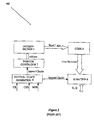
- the block diagram of a RAM memory is shown in Figure 1, globally indicated with M1. More particularly, the memory M1 comprises a decoder section 1, a core section 2, an IO section 4 and a control / clock generation section 3.
- the decoder section 1 receives internal clocks from the control / clock generation section 3 as well as a datum A outside of the memory M1 and is connected to the core 2 by a plurality of word lines.
- the core 2 is in turn connected to the 10 section 4 by a plurality of core bit lines, the IO section 4 receiving a plurality of internal clocks from the control / clock generation section 3 as well.
- control / clock generation section 3 receives control signals, such as the well known signals CSN, WEN...
- the IO section 4 is connected outside of the memory M1 in a bidirectional manner and provides/receives signals indicated as D, Q in the figure.
- Various electronic blocks or elements like X Decoder, Y Decoder, Pre Decoder, Core, I/O's / Precharge / Read / Write Logic, Clock Generation Circuits, Dummy Paths, Refresh Logic and Pipe Lines are made in form of leaf cells that are abutted to form a memory block of a desired "word x bit" configuration.
- the full memory development thus pertains to making these leaf cells with a new technology and tuning them according to the full range of words and bits provided.
- the decoder section 1 of the memory usually comprises latches to latch address inputs.
- the addresses are statically decoded and a valid decoded value is clocked to finally select a row or column (or both) to write onto or read from the corresponding cells.
- row selection signals called "wordlines” are subjected to a precharge mechanism using an internally generated memory clock.
- the write unit of the memory can be as simple as a latch to store the value at a data input port on the positive edge of the clock, and a strong buffer to pull the column selection signals called "bitlines” (which are architecture specific) to the latched value.
- a writing operation of a DRAM involves a more complex structure as the data to be written on a row is first copied on to a row register and then written into the memory. Periodic refresh cycles are simply read write operations of the DRAM memory cells.
- the reading circuit can be as simple as a digital inverter Lu sense the discharge of a precharged bitline or as complex as a differential / latch type, single / double ended sense amplifier which is analog in nature.
- the reading operation is complex as the reading is destructive.
- a latch can be used to hold the value read out from the memory in a particular cycle, until the next operation at the next positive edge of the memory clock.
- the core 2 can comprises a group of cells, which can be single latches, or six, four, eight transistor complex latches or a capacitor.
- a second type of memory architecture which is known as a "register file” typically comprises data input ports and address ports for writing operations, data output ports and address ports for reading operations (in case of FIFOs or stacks there are no address ports), an IO section, decoders or counters, pipelines, clock generation circuits (in case of a self timed architecture) and refresh logic.
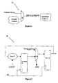
- the block diagram of such a register file memory is shown in Figure 2, globally indicated with M2.
- the memory M2 comprises a decoder section 5, a core 6, a pointer generator 7, a control / clock generation section 8 and an IO section 9.
- the decoder section 5 receives address signals from pointer generator 7 and is connected to the core 6 by a plurality of word lines.
- the core 6 is in turn connected to the IO section 6 by a plurality of core bit lines, the IO section 9 receiving a plurality of internal clocks from the control / clock generation section 3.
- control / clock generation section 9 receives control signals, such as the well known signals CSN, WEN... and a clock signal CK and provides a plurality of internal clocks to the pointer generator 7.
- the IO section 9 is connected outside of the memory M2 in a bidirectional manner and provides/receives signals indicated as D, Q in the figure.
- a typical structure of this kind of memories in addition to a structure of a normal memory, comprises:
- a decoder of the register file contains latches for the address and data inputs, write enable or read enable signals.
- FIFOs or LIFOs there are no address ports as the memory self-generates the addresses sequentially.
- address ports addresses arc statically or dynamically decoded and the valid decoded value is clocked to finally select a row or column (or both) to write onto or read from the corresponding cells.
- Dynamic decoders work in the similar fashion as described above with reference to single port memories.
- the pointer generation in the register file memory is a complex operation.
- a FIFO there are generally two pointers, one is for the reading operations and the other is for the writing operations.
- the position of the write pointer coincides with the position of the read pointer.
- the write pointer marches ahead of the read pointer making space for the read pointer to move further.
- the FIFO becomes full when the write pointer comes exactly one location behind the read pointer. In this condition further writing operations cannot be performed.
- half full cases or half empty cases are also generated.
- the read pointer and the write pointer are compared to find their equality.
- To generate a Full flag the write pointer is compared to the read pointer to determine if the write pointer value is one less than the read pointer value.
- the major difficulty arises due to the fact that the clocks for the read and write pointers are normally different. In the aforesaid case, the flags act as synchronization signals for the two clock domains.
- the present invention aims at providing a memory architecture, which solves all the above outlines problems simultaneously and does overcome the above-mentioned disadvantages of the known memory architectures.
- the solution idea underlying the present invention is that of providing a memory architecture with a built-in testing mechanism integrated in the memory architecture.
- the invention generally relates to a high-speed memory architecture, which uses a built-in structured DFT (Design-for-Testability) technique to test itself, thus reducing the effort of using DIST or any other DFT technique. In this way, the user is saved from putting extra efforts in timing analysis twice, as in the known solutions. The effort of BIST insertion is also reduced.
- DFT Design-for-Testability
- the memory architecture of the present invention is a complete memory solution for a high-speed embedded RAM that has been designed while keeping the testing aspect in mind, thus resulting in an efficient architecture.
- the memory architecture according to the invention is shown in Figure 3, globally indicated with M. It should be noted that the memory architecture M comprises test pins along with minimal hardware, which are added to a classical memory interface. In particular, through the test pins indicated as TESTSE, TESTSI & TESTSO a test mechanism is configured inside the memory architecture itself.
- the memory architecture M also comprises a TEST pin which is used to distinguish between a functional mode (transparent mode) and a test mode.
- the memory architecture M comprises a decoder section 10, a core 11 and an IO section 12.
- the decoder section 10 receives a latched address signal A_lat as well as internal clocks from the IO section 12 and is connected to the core 11 by a plurality of word lines.
- the core 11 is in turn connected to the 10 section 12 by a plurality of core bit lines.
- the decoder section 10 thus comprises at least one decoder.
- the IO section 12 comprises a System Multiplexer 13 connected to the TEST pin, a Compressor 14 connected to a Comparator 16 and a Data/Pattern Generator 15 providing the System Multiplexer 13 with an inner data signal D_int.
- the System Multiplexer 13 also receives control signals CSN and WEN and an input data signal D. Furthermore, the IO section 12 provides an output data signal Q.
- the memory architecture M further comprises a Control Block 18 receiving a clock signal CK, a reset signal RSTN and a test signal TEST through the TEST pin.
- the Control Block 18 comprises a FSM (Finite State Machine) 17 connected to the Comparator 16 to which it provides a first polarity signal Q_polarity as well as to the Data/Pattern Generator 15 to which it provides a second polarity signal D_polarity.
- the FSM 17 is also connected to the System Multiplexer 13 and provides it with inner control signals CSN_int and WEN_int.
- Control Block 18 is connected to a Complexor 19 of an Address Generator 24 which receives the clock signal CK.
- the Complexor 19 is also connected to the System Multiplexer 13 of the IO section 12 and provide it with an inner address signal A_int.
- the System Multiplexer 13 is configured using tristate buffers.
- the memory architecture M comprises a Serial Interface 25 connected to the test pins, TESTSI, TESTSE and TESTSO, and receiving a serial shift clock.
- the Serial Interface 25 is also connected to the Comparator 16 and to the Control Block 18 to which it provides control inputs.
- the Compressor 14 has an output line 20 connected to the Comparator 16 and providing a compressed output signal
- the Comparator 16 has an output line 21 connected to the Serial Interface 25 and providing BBAD and STATUS signals
- the Control Block 18 ha an output line 22 providing a BEND signal
- the Complexor 19 has an output line 23 connected to the Control Block 18 and providing an information signal.
- the memory architecture M has an integrated built-in testing mechanism and essentially comprises:
- the I/O Section 12 and the Control Block 18 are enhanced to be configurable for built-in testing in test mode by comprising:
- a data to be run is programmed in the Serial Interface 25.
- This data consists of information like, pattern type, number of operations, type of operations, address directions, LFSR seed etc. and is shifted at the speed of the serial shift clock received by the Serial Interface 25, through serial inputs.
- the TEST pin is made high, to activate the FSM 17, which generates various controls for the other blocks based upon the control inputs from the Serial Interface 25.
- the Address Generator 24 generates the address, based upon FSM 17 controls and Serial Interface 25 controls like, initial address and final value, address direction, LFSR seed.
- Data/Pattern Generator 15 generates the data inputs based upon the FSM 17 controls and serial interface controls like data polarity, data background, scrambling information from the address generator, data pattern type etc.
- the Data/Pattern Generator 15 generates the controls based upon the FSM 17 controls and serial interface 25 controls like operations to be performed (reading/writing operations), memory to be selected or not and the required port to be activated.
- Complexor 19 creates difference between various port addresses in case a duplex operation or a multiplex operation is to be performed.
- the Complexor 19 in a multi port memory configuration is used to synchronize test operations over multiple ports and to perform simultaneous operations on the multi-port memory.
- the Compressor 14 compresses the memory output and Comparator 16 compares at each valid output data signalled by the FSM 17. The result is either brought directly at the memory output or loaded in the Scrial Interface 25. In other words, the Compressor 14 compresses the data prior to forwarding to the Comparator 16.
- the System Multiplexer 13 selects the Memory functional inputs coming from the system or the test inputs generated from the embedded test circuitry.
- the System Multiplexer 13 thus multiplexes external address bus and internal test address bus.
- Serial Interface 25 can be configured like above and then the embedded circuitry can run the test on the memory, and generate status for each test and pass it to the Serial Interface 25.
- connection of various sub-blocks blocks can be adjusted according to the memory architecture.
- the address decoder as well as control unit of the memory are usually on one side of the memory.
- the Address Generator 24 is put just below the address decoder to minimize the routing and connection overhead. This also makes the address generation faster as there are lesser interconnect delays.
- the Compressor 14 and the Comparators 16 can be put per page while the Address Generators 24, FSM 17 and other logic can be shared or duplicated for each page as per the speed needed.
- DRAM Paged memory architecture
- FIG 4 shows in greater detail the System Multiplexer 13 of the memory architecture M according to the present invention.
- the System Multiplexer 13 is connected to the system pins and the test inputs for receiving the memory address and test address generated by the Complexor 19.
- a multiplexer 26 of the System Multiplexer 13 according to the invention is connected to the external TEST pin and receives an enable signal therefrom.
- a similar multiplexer configuration is used for the memory pins interacting with the system. These multiplexers are technology independent and minimum number of the same is required as they result in additional delay in the setup time of the memory architecture.
- the Serial Interface 25 is used to shift data in the test mode.
- the data to be shifted may include the type and the number of operations to be performed on each address, the seed of the Linear Feedback Shift Register (LFSR), the data to be written on the memory, the data pattern (checkerboard, stripes etc.), the memory section on which the test has to be run, etc.
- LFSR Linear Feedback Shift Register
- the serial shift clock can be any clock depending upon the usage and the environment.
- the Serial Interface 25 may be internal or external to the memory and can be shared between several memories. The information is shifted in serially at a very low clock speed.
- Figure 5 shows in greater detail the Address Generator 24 which is used for generating the test address for the memory and is therefore a Test Address Generator. Deterministic, exhaustive or pseudo-random counters are used for address generation.
- Serial Interface 25 can be used to configure the Address Generator 24 to produce a particular sequence of addresses. This helps in detecting the memory faults that are sequence dependent.
- the Address Generator 24 can also be configured to produce a single address for writing galloping patterns etc.
- the Address Generator 24 comprises a logic 27 receiving a COUNT signal and connected to a master latch 28, which receives the clock signal CK and is connected to a multiplexer 26A, in turn receiving a system address signal and being connected to a slave latch 30.
- the slave latch 30 receives the clock signal CK and has an output feedback connected to the logic 27.
- Address Generator 24 provides additional test reliability being made using the memory latches already present inside the memory.
- the memory latch acts as a slave latch 30 and is combined with the master latch 28 present in the test unit to form a scanable Flip-Flop.
- the system observability is increased by putting a scan multiplexer on the buses and signals coming from the system.
- this arrangement increases the testability of the memory and reduces the required area for the Address Generator 24.
- the same arrangement is used for the other pins like, write enable, read enable, data ports etc.
- pointers are generated normally in gray codcs due to which the fault model uf such a FIFO is different from a memory, which is counting in Binary Coded Decimal.
- the operation of a test sequence for one location may not be totally linked with the operation on the next location. But then testing with any other sequence will be irrelevant and it may lead to over testing or under testing.
- Using the pointer of the memory itself also saves a lot of arca.
- the Data Generator 15 generates the data based on the data polarity signal D_polarity and sequence configured through the Serial Interface 25.
- the Address Generator 24 is responsible for producing all test patterns for comprehensive testing of the memory and is therefore also a Test Pattern Generator.
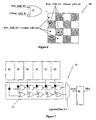
- checkerboard pattern CB is done by using a single XOR gate 31 for generic row column based memory as shown in Figure 6.
- the XOR gate 31 is thus a Test Pattern Generator.
- the Test Pattern Generator 31 is realised by a Linear Feedback Shift Register.
- the data latch of the memory are turned into the Flip-Flops by adding a master latch to the address generator, thus resulting the in a very high-speed memory test. Additionally, as these Flip-Flops are scannable they add observability on the input data pins from the memory.
- the Control Block 18 generates control signals for testing of the memory. These control signals include signals for read or write operations on the memory, reset signals for the memory state machine, disable control signal for the memory self time control, etc.
- control signals are generated during the run time in the test mode. Similar to other blocks, the control latches are changed to flipflops and hence, the observability is increased on the system pins. These control inputs are controlled through the FSM 17.
- Control Block 18 controls the operation from all the ports in case of simultaneous operations. Also all the ports can have the same address on their address inputs but the control of operation is done through this port.
- Control Block 18 In case of a read through a port while writing, the Control Block 18 generates a signal, which stops the comparison of the output data, as the read operation is invalid.
- the Control Block 18 is advantageously programmed though the Serial Interface 25 for any control generation.
- the FSM 17 is responsible for controlling all activities for the test device. On receiving a high signal at the TEST pin, the FSM 17 resets and initializes all the registers in other blocks of the test device.
- setting TEST enable pin low synchronously resets the FSM 17 to initial state in next clock cycle.
- the FSM 17 is designed in a gray code (two neighbor states differ by only one bit).
- the states in the State machine are n bits wide where n depends on the number of address sequences tested in one run.
- the value and type of the sequences run on the memory are advantageously configured through the Serial Interface 25 serially.
- the FSM 17 is only responsible for counting the number of such sequences and responsible for activating or deactivating each block in an ITSME device by controlling the control generator for generating various control signals.
- An external signal BEND is set high after all the test sequences have been applied on the memory. This is an indication that the configured series of sequences have been applied and further tests can be carried by configuring new sequences.
- the Compressor 14 is used for compressing the data before comparison to reduce the size of the comparator.
- the Compressor 14 can be as simple as a Multiple Input Signature Register (MISR), which compresses the output to a known signature configured through the Serial Interface 25.
- MISR Multiple Input Signature Register
- the MISRs are also made by changing the memory output latch to a Flip-Flop in the self-test mode.
- a MISR polynomial compresses the selected data bit outputs to a single signature.
- the MISR polynomial is configurable and is chosen based on the data bit length for the test purpose, which can also be advantageously configured through Serial Interface 25. Thus different types of debugging are also possible by configuring a suitable MISR polynomial.
- the Compressor 14 is made very small making it more suitable for the memories where test algorithms are mostly deterministic.
- the data output either consists of checkerboard or a solid pattern or a known repeated patterns. These are first compressed to all zeros or all ones, by using NAND - NOR chains.
- the Compressor 14 is essentially a chain of logic gates.
- Different techniques and logics can be used but at the end all the data outputs are compressed to a single bit, which is compared with the expected data bit.
- the different compressors are used based on the memory floor plan and architecture. To save area, the compressors can be shared between various pages of the memory as well.
- the Comparator 16 compares the compressed data, either a signature or a deterministic set of bits, with a golden signature or known data, which is received from the Serial Interface 25.
- the signature comparison normally happens at the end of a test run, but the deterministic data comparison can happen on every cycle.
- the FSM 17 provides the expected data on each clock cycle, which is advantageously configured through the Serial Interface 25.
- FIG. 7 The schematic of a generic Compressor 14 and Comparator 16 is shown in Figure 7.
- the figure illustratcs the case where the memory is filled with either all zeros or all ones.
- the output Q bus is still all zeroes or all ones and comparison is easily done using a NAND-OR chain. If the Q output bus itself has a checkerboard or repeated patterns, then NAND-OR blocks can be used for all odd bits and even bits separately without putting any extra logic.
- the Compressor 14 logic does not increase based on the complexity of the repeated data background.
- the pattern itself is given on the D system bus and the expected data is generated by XORing the pattern present on the D input bus of the memory, with Q output bus to produce all zeros or all ones. After this, compression is done to get a single bit in the same manner.
- This method involves putting a particular pattern on the D bus, which can increase the testing time by shifting the D patterns on the D bus.
- This type of pattern (galloping) is good for debugging purposes.
- a good testable device always has a proper mechanism for initialization of all blocks on the device. All the sequential devices on a chip must be resetable and must contain known data on all blocks before test. To achieve this inside the architecture has a dedicated unit called Unit for reset management (URM).
- UPM Unit for reset management
- This unit is used for asynchronous Reset / Preset of the full memory including all the flip-flops, latches and the core of the memory through a Reset pin (active low). It is also used to initialize the memory with checkerboard pattern or a known pattern present on the D bus.
- Figure 5 shows in greater detail the Complexor 19 which is primarily used with the register file memories.
- the Complexor 19 is used to synchronize patterns in case of a simultaneous operation on nearby locations, more than one port.
- the Complexor 19 comprises two basic parts, namely an Address Filter and a Qpolarity Filter.
- the Address Filter generates addresses of various ports based upon the configuration. For example, if there are three ports (two read and one write), then there can be nine possible arrangements of the ports in terms of their start addresses, which can be easily calculated, based upon the permutation/combination.
- the sequence of the ports can be calculated based upon the difference of the port address from the first port address. Though this leads to duplicity but it reduces a lot of area, as this information is low speed information.
- the difference between one port and the other port should not be greater than a programmed value, which is normally 1 to get better coverage, but it can be at most 2.
- the Qpolarity Filter is needed as the address ports run in a rotation. When there is a difference between the port addresses, all the ports count the same number of addresses.
- the qpolarity is the polarity of data written previously on a location or in some previous clock cycle. This is the data expected on that location.
- the qpolarity filter thus generates a complex expected data based upon the port difference and port sequence coming from the Serial Interface 25.
- the method for in-built testing of configurable memory architecture comprises the following steps of:
- the memory architecture according to the invention is a solution worth using inside the embedded memories whether they are asynchronous or synchronous, static or dynamic, soft or hard.
- the key point of this invention is that it treats the memory not as a macro but moves inside to see the things in detail.
- no external BIST are to be put inside a chip to test the memory.
- testability is increased and the full memory is no more a black box. Only the core, which is treated, as black box is isolated during test.
- the proposed memory architecture is aimed to a better access and cycle time and having a very little impact on address setup and hold with respect to clock.
- the power consumption is nearly the same.
- test patterns including the self test
- the need for a sophisticated tester is also eliminated as all the test patterns (including the self test) are generated with in the chip itself or it can be done through a simple TAP or P1500 or some other serial or parallel interface.
- a memory architecture with a highly optimized in-built testing mechanism in terms of area and speed is provided.
- system level testability is increased and the memory core is reset as well as the memory is initialised with a known pattern.
- the present invention relates to configurable memory architecture with a built-in testing mechanism integrated in the memory to support very efficient built-in self-test in Random Access Memories (RAMs) with greatly reduced overhead, in terms of area and speed.
- RAMs Random Access Memories
- Memories can fail at high speed due to glitches (unwanted pulses which can at times behave as invalid clocks and destroy the functionality of synchronous systems) produced in decoding, the slow precharge of bitlines or the slow sensing of the sense amplifiers.
- the proposed memory architecture incorporates structured DFT techniques to detect all these failure separately.
Landscapes
- Tests Of Electronic Circuits (AREA)
- For Increasing The Reliability Of Semiconductor Memories (AREA)
- Techniques For Improving Reliability Of Storages (AREA)
Applications Claiming Priority (1)
| Application Number | Priority Date | Filing Date | Title |
|---|---|---|---|
| IN1405DE2005 | 2005-05-31 |
Publications (2)
| Publication Number | Publication Date |
|---|---|
| EP1732082A2 true EP1732082A2 (de) | 2006-12-13 |
| EP1732082A3 EP1732082A3 (de) | 2007-11-21 |
Family
ID=36930257
Family Applications (1)
| Application Number | Title | Priority Date | Filing Date |
|---|---|---|---|
| EP06011188A Withdrawn EP1732082A3 (de) | 2005-05-31 | 2006-05-31 | Speicherarchitektur mit BIST |
Country Status (2)
| Country | Link |
|---|---|
| US (1) | US7603603B2 (de) |
| EP (1) | EP1732082A3 (de) |
Families Citing this family (22)
| Publication number | Priority date | Publication date | Assignee | Title |
|---|---|---|---|---|
| KR100771875B1 (ko) * | 2006-07-10 | 2007-11-01 | 삼성전자주식회사 | 테스트하고자 하는 메모리 셀의 개수를 임의로 설정할 수있는 반도체 메모리 장치 및 반도체 메모리 장치의 테스트방법 |
| JP4939870B2 (ja) * | 2006-08-16 | 2012-05-30 | 株式会社東芝 | 半導体記憶装置およびそのテスト方法 |
| US20080148119A1 (en) * | 2006-12-19 | 2008-06-19 | National Tsing Hua University | Apparatus for Built-in Speed Grading and Method for Generating Desired Frequency for the Same |
| US8144170B2 (en) * | 2007-03-28 | 2012-03-27 | Himax Technologies Limited | Apparatus for scaling image and line buffer thereof |
| US8214699B2 (en) * | 2008-06-27 | 2012-07-03 | International Business Machines Corporation | Circuit structure and method for digital integrated circuit performance screening |
| JP5556809B2 (ja) * | 2009-03-30 | 2014-07-23 | 日本電気株式会社 | 情報処理システム、情報圧縮装置、情報復元装置、情報処理方法及びそのプログラム |
| US20120236660A1 (en) * | 2011-03-16 | 2012-09-20 | Nanya Technology Corp. | Test system and test method for memory |
| US8239818B1 (en) | 2011-04-05 | 2012-08-07 | International Business Machines Corporation | Data structure for describing MBIST architecture |
| US8627158B2 (en) | 2011-12-08 | 2014-01-07 | International Business Machines Corporation | Flash array built in self test engine with trace array and flash metric reporting |
| KR20130134610A (ko) * | 2012-05-31 | 2013-12-10 | 에스케이하이닉스 주식회사 | 반도체 메모리 장치 및 그것의 테스트 방법 |
| US20130326281A1 (en) * | 2012-06-01 | 2013-12-05 | Syntest Technologies, Inc. | X-Tracer: A Reconfigurable X-Tolerance Trace Compressor for Silicon Debug |
| US9773570B2 (en) * | 2013-03-06 | 2017-09-26 | International Business Machines Corporation | Built-in-self-test (BIST) test time reduction |
| US9263100B2 (en) | 2013-11-29 | 2016-02-16 | Freescale Semiconductor, Inc. | Bypass system and method that mimics clock to data memory read timing |
| KR102193885B1 (ko) * | 2014-01-17 | 2020-12-22 | 삼성전자주식회사 | 감지 증폭기 및 이를 포함하는 메모리 장치 |
| US9218862B1 (en) | 2014-04-11 | 2015-12-22 | Altera Corporation | Method and apparatus for operating finite-state machines in configurable storage circuits |
| US10095474B2 (en) * | 2014-05-05 | 2018-10-09 | Texas Instruments Incorporated | Filler bank control circuit for synchronous FIFO queues and other memory devices |
| US9281081B1 (en) * | 2014-11-10 | 2016-03-08 | SK Hynix Inc. | Built-in test circuit of semiconductor apparatus |
| US10438678B2 (en) * | 2017-04-04 | 2019-10-08 | Globalfoundries Inc. | Zero test time memory using background built-in self-test |
| US10247780B2 (en) | 2017-08-02 | 2019-04-02 | Texas Instruments Incorporated | Re-programmable self-test |
| US11082241B2 (en) * | 2018-03-30 | 2021-08-03 | Intel Corporation | Physically unclonable function with feed-forward addressing and variable latency output |
| US11379376B2 (en) | 2020-05-20 | 2022-07-05 | Micron Technologies, Inc. | Embedding data in address streams |
| US12362028B2 (en) * | 2022-09-06 | 2025-07-15 | Taiwan Semiconductor Manufacturing Company, Ltd. | Memory test circuit, memory chip, and testing method of memory chip |
Family Cites Families (11)
| Publication number | Priority date | Publication date | Assignee | Title |
|---|---|---|---|---|
| US5258986A (en) * | 1990-09-19 | 1993-11-02 | Vlsi Technology, Inc. | Tightly coupled, low overhead RAM built-in self-test logic with particular applications for embedded memories |
| US5872794A (en) * | 1994-09-30 | 1999-02-16 | Texas Instruments Incorporated | Flash EPROM control with embedded pulse timer and with built-in signature analysis |
| JP2001014890A (ja) * | 1999-06-30 | 2001-01-19 | Mitsubishi Electric Corp | 半導体装置および半導体装置のテスト方法 |
| US7111190B2 (en) * | 2001-02-23 | 2006-09-19 | Intel Corporation | Method and apparatus for reconfigurable memory |
| US6888776B2 (en) * | 2000-09-06 | 2005-05-03 | Renesas Technology Corp. | Semiconductor memory device |
| JP3751576B2 (ja) * | 2002-05-28 | 2006-03-01 | 沖電気工業株式会社 | 半導体装置及びそのテスト方法 |
| JP2004199842A (ja) * | 2002-12-20 | 2004-07-15 | Nec Micro Systems Ltd | 半導体記憶装置及びその制御方法 |
| US7020820B2 (en) * | 2002-12-20 | 2006-03-28 | Sun Microsystems, Inc. | Instruction-based built-in self-test (BIST) of external memory |
| JP3863124B2 (ja) * | 2003-05-08 | 2006-12-27 | 株式会社東芝 | 半導体記憶装置及びそのテスト方法 |
| JP4105077B2 (ja) * | 2003-10-30 | 2008-06-18 | 株式会社東芝 | 半導体集積回路 |
| US7225379B2 (en) * | 2004-04-23 | 2007-05-29 | Oki Electric Industry Co., Ltd. | Circuit and method for testing semiconductor device |
-
2006
- 2006-05-26 US US11/441,815 patent/US7603603B2/en not_active Expired - Fee Related
- 2006-05-31 EP EP06011188A patent/EP1732082A3/de not_active Withdrawn
Also Published As
| Publication number | Publication date |
|---|---|
| EP1732082A3 (de) | 2007-11-21 |
| US20070016826A1 (en) | 2007-01-18 |
| US7603603B2 (en) | 2009-10-13 |
Similar Documents
| Publication | Publication Date | Title |
|---|---|---|
| US7603603B2 (en) | Configurable memory architecture with built-in testing mechanism | |
| US6668347B1 (en) | Built-in self-testing for embedded memory | |
| KR970004074B1 (ko) | 메모리 장치 및 이를 포함한 집적 회로 | |
| US7729185B2 (en) | Apparatus and method for detection of address decoder open faults | |
| US7721174B2 (en) | Full-speed BIST controller for testing embedded synchronous memories | |
| US5258986A (en) | Tightly coupled, low overhead RAM built-in self-test logic with particular applications for embedded memories | |
| US8156391B2 (en) | Data controlling in the MBIST chain architecture | |
| US8780648B2 (en) | Latch based memory device | |
| KR20060043690A (ko) | 테스트 회로, 그 테스트 회로를 내장한 반도체집적회로장치및 그 테스트 방법 | |
| US6510530B1 (en) | At-speed built-in self testing of multi-port compact sRAMs | |
| US7971117B2 (en) | Test circuits of semiconductor memory device for multi-chip testing and method for testing multi chips | |
| JPS63102098A (ja) | 集積回路 | |
| US6671836B1 (en) | Method and apparatus for testing memory | |
| TWI419170B (zh) | 積體電路以及用於測試該電路之方法 | |
| US20050152190A1 (en) | Semiconductor memory device capable of testing memory cells at high speed | |
| EP1727156B1 (de) | Verbesserte bereichseffiziente Speicherarchitektur mit Dekoderautotest und Debug-Fähigkeit | |
| US6430072B1 (en) | Embedded CAM test structure for fully testing all matchlines | |
| US20080013389A1 (en) | Random access memory including test circuit | |
| US20030182607A1 (en) | Semiconductor memory device and method of testing same | |
| CA2426040A1 (en) | At-speed built-in self testing of multi-port compact srams | |
| Nicolaidis et al. | Trade-offs in scan path and BIST implementations for RAMs | |
| US12424296B2 (en) | Circuit for testing memories | |
| US20020138797A1 (en) | Method of testing a sequential access memory plane and a corresponding sequential access memory semiconductor device | |
| JP2005129174A (ja) | メモリ自己検査機能を有する半導体装置 | |
| Amin et al. | Efficient O (� n) BIST Algorithms for DDNPS Faults in Dual-Port Memories |
Legal Events
| Date | Code | Title | Description |
|---|---|---|---|
| PUAI | Public reference made under article 153(3) epc to a published international application that has entered the european phase |
Free format text: ORIGINAL CODE: 0009012 |
|
| AK | Designated contracting states |
Kind code of ref document: A2 Designated state(s): AT BE BG CH CY CZ DE DK EE ES FI FR GB GR HU IE IS IT LI LT LU LV MC NL PL PT RO SE SI SK TR |
|
| AX | Request for extension of the european patent |
Extension state: AL BA HR MK YU |
|
| PUAL | Search report despatched |
Free format text: ORIGINAL CODE: 0009013 |
|
| AK | Designated contracting states |
Kind code of ref document: A3 Designated state(s): AT BE BG CH CY CZ DE DK EE ES FI FR GB GR HU IE IS IT LI LT LU LV MC NL PL PT RO SE SI SK TR |
|
| AX | Request for extension of the european patent |
Extension state: AL BA HR MK YU |
|
| 17P | Request for examination filed |
Effective date: 20080520 |
|
| AKX | Designation fees paid |
Designated state(s): DE FR GB IT |
|
| 17Q | First examination report despatched |
Effective date: 20080703 |
|
| STAA | Information on the status of an ep patent application or granted ep patent |
Free format text: STATUS: THE APPLICATION IS DEEMED TO BE WITHDRAWN |
|
| 18D | Application deemed to be withdrawn |
Effective date: 20090114 |