EP1732111A1 - Suszeptor - Google Patents
Suszeptor Download PDFInfo
- Publication number
- EP1732111A1 EP1732111A1 EP05721602A EP05721602A EP1732111A1 EP 1732111 A1 EP1732111 A1 EP 1732111A1 EP 05721602 A EP05721602 A EP 05721602A EP 05721602 A EP05721602 A EP 05721602A EP 1732111 A1 EP1732111 A1 EP 1732111A1
- Authority
- EP
- European Patent Office
- Prior art keywords
- susceptor
- barrel type
- disposed
- internal
- substrates
- Prior art date
- Legal status (The legal status is an assumption and is not a legal conclusion. Google has not performed a legal analysis and makes no representation as to the accuracy of the status listed.)
- Withdrawn
Links
Images




Classifications
-
- H—ELECTRICITY
- H10—SEMICONDUCTOR DEVICES; ELECTRIC SOLID-STATE DEVICES NOT OTHERWISE PROVIDED FOR
- H10P—GENERIC PROCESSES OR APPARATUS FOR THE MANUFACTURE OR TREATMENT OF DEVICES COVERED BY CLASS H10
- H10P72/00—Handling or holding of wafers, substrates or devices during manufacture or treatment thereof
- H10P72/70—Handling or holding of wafers, substrates or devices during manufacture or treatment thereof for supporting or gripping
- H10P72/76—Handling or holding of wafers, substrates or devices during manufacture or treatment thereof for supporting or gripping using mechanical means, e.g. clamps or pinches
- H10P72/7604—Handling or holding of wafers, substrates or devices during manufacture or treatment thereof for supporting or gripping using mechanical means, e.g. clamps or pinches the wafers being placed on a susceptor, stage or support
- H10P72/7624—Handling or holding of wafers, substrates or devices during manufacture or treatment thereof for supporting or gripping using mechanical means, e.g. clamps or pinches the wafers being placed on a susceptor, stage or support characterised by the mechanical construction of the susceptor, stage or support
-
- C—CHEMISTRY; METALLURGY
- C23—COATING METALLIC MATERIAL; COATING MATERIAL WITH METALLIC MATERIAL; CHEMICAL SURFACE TREATMENT; DIFFUSION TREATMENT OF METALLIC MATERIAL; COATING BY VACUUM EVAPORATION, BY SPUTTERING, BY ION IMPLANTATION OR BY CHEMICAL VAPOUR DEPOSITION, IN GENERAL; INHIBITING CORROSION OF METALLIC MATERIAL OR INCRUSTATION IN GENERAL
- C23C—COATING METALLIC MATERIAL; COATING MATERIAL WITH METALLIC MATERIAL; SURFACE TREATMENT OF METALLIC MATERIAL BY DIFFUSION INTO THE SURFACE, BY CHEMICAL CONVERSION OR SUBSTITUTION; COATING BY VACUUM EVAPORATION, BY SPUTTERING, BY ION IMPLANTATION OR BY CHEMICAL VAPOUR DEPOSITION, IN GENERAL
- C23C16/00—Chemical coating by decomposition of gaseous compounds, without leaving reaction products of surface material in the coating, i.e. chemical vapour deposition [CVD] processes
- C23C16/44—Chemical coating by decomposition of gaseous compounds, without leaving reaction products of surface material in the coating, i.e. chemical vapour deposition [CVD] processes characterised by the method of coating
- C23C16/458—Chemical coating by decomposition of gaseous compounds, without leaving reaction products of surface material in the coating, i.e. chemical vapour deposition [CVD] processes characterised by the method of coating characterised by the method used for supporting substrates in the reaction chamber
- C23C16/4582—Rigid and flat substrates, e.g. plates or discs
- C23C16/4587—Rigid and flat substrates, e.g. plates or discs the substrate being supported substantially vertically
- C23C16/4588—Rigid and flat substrates, e.g. plates or discs the substrate being supported substantially vertically the substrate being rotated
-
- C—CHEMISTRY; METALLURGY
- C30—CRYSTAL GROWTH
- C30B—SINGLE-CRYSTAL GROWTH; UNIDIRECTIONAL SOLIDIFICATION OF EUTECTIC MATERIAL OR UNIDIRECTIONAL DEMIXING OF EUTECTOID MATERIAL; REFINING BY ZONE-MELTING OF MATERIAL; PRODUCTION OF A HOMOGENEOUS POLYCRYSTALLINE MATERIAL WITH DEFINED STRUCTURE; SINGLE CRYSTALS OR HOMOGENEOUS POLYCRYSTALLINE MATERIAL WITH DEFINED STRUCTURE; AFTER-TREATMENT OF SINGLE CRYSTALS OR A HOMOGENEOUS POLYCRYSTALLINE MATERIAL WITH DEFINED STRUCTURE; APPARATUS THEREFOR
- C30B25/00—Single-crystal growth by chemical reaction of reactive gases, e.g. chemical vapour-deposition growth
- C30B25/02—Epitaxial-layer growth
- C30B25/12—Substrate holders or susceptors
-
- C—CHEMISTRY; METALLURGY
- C30—CRYSTAL GROWTH
- C30B—SINGLE-CRYSTAL GROWTH; UNIDIRECTIONAL SOLIDIFICATION OF EUTECTIC MATERIAL OR UNIDIRECTIONAL DEMIXING OF EUTECTOID MATERIAL; REFINING BY ZONE-MELTING OF MATERIAL; PRODUCTION OF A HOMOGENEOUS POLYCRYSTALLINE MATERIAL WITH DEFINED STRUCTURE; SINGLE CRYSTALS OR HOMOGENEOUS POLYCRYSTALLINE MATERIAL WITH DEFINED STRUCTURE; AFTER-TREATMENT OF SINGLE CRYSTALS OR A HOMOGENEOUS POLYCRYSTALLINE MATERIAL WITH DEFINED STRUCTURE; APPARATUS THEREFOR
- C30B31/00—Diffusion or doping processes for single crystals or homogeneous polycrystalline material with defined structure; Apparatus therefor
- C30B31/06—Diffusion or doping processes for single crystals or homogeneous polycrystalline material with defined structure; Apparatus therefor by contacting with diffusion material in the gaseous state
- C30B31/14—Substrate holders or susceptors
-
- H—ELECTRICITY
- H10—SEMICONDUCTOR DEVICES; ELECTRIC SOLID-STATE DEVICES NOT OTHERWISE PROVIDED FOR
- H10P—GENERIC PROCESSES OR APPARATUS FOR THE MANUFACTURE OR TREATMENT OF DEVICES COVERED BY CLASS H10
- H10P72/00—Handling or holding of wafers, substrates or devices during manufacture or treatment thereof
- H10P72/04—Apparatus for manufacture or treatment
- H10P72/0431—Apparatus for thermal treatment
- H10P72/0432—Apparatus for thermal treatment mainly by conduction
-
- H—ELECTRICITY
- H10—SEMICONDUCTOR DEVICES; ELECTRIC SOLID-STATE DEVICES NOT OTHERWISE PROVIDED FOR
- H10P—GENERIC PROCESSES OR APPARATUS FOR THE MANUFACTURE OR TREATMENT OF DEVICES COVERED BY CLASS H10
- H10P72/00—Handling or holding of wafers, substrates or devices during manufacture or treatment thereof
- H10P72/70—Handling or holding of wafers, substrates or devices during manufacture or treatment thereof for supporting or gripping
- H10P72/76—Handling or holding of wafers, substrates or devices during manufacture or treatment thereof for supporting or gripping using mechanical means, e.g. clamps or pinches
- H10P72/7604—Handling or holding of wafers, substrates or devices during manufacture or treatment thereof for supporting or gripping using mechanical means, e.g. clamps or pinches the wafers being placed on a susceptor, stage or support
- H10P72/7616—Handling or holding of wafers, substrates or devices during manufacture or treatment thereof for supporting or gripping using mechanical means, e.g. clamps or pinches the wafers being placed on a susceptor, stage or support characterised by a coating, a hardness or a material
-
- H—ELECTRICITY
- H10—SEMICONDUCTOR DEVICES; ELECTRIC SOLID-STATE DEVICES NOT OTHERWISE PROVIDED FOR
- H10P—GENERIC PROCESSES OR APPARATUS FOR THE MANUFACTURE OR TREATMENT OF DEVICES COVERED BY CLASS H10
- H10P72/00—Handling or holding of wafers, substrates or devices during manufacture or treatment thereof
- H10P72/70—Handling or holding of wafers, substrates or devices during manufacture or treatment thereof for supporting or gripping
- H10P72/76—Handling or holding of wafers, substrates or devices during manufacture or treatment thereof for supporting or gripping using mechanical means, e.g. clamps or pinches
- H10P72/7604—Handling or holding of wafers, substrates or devices during manufacture or treatment thereof for supporting or gripping using mechanical means, e.g. clamps or pinches the wafers being placed on a susceptor, stage or support
- H10P72/7621—Handling or holding of wafers, substrates or devices during manufacture or treatment thereof for supporting or gripping using mechanical means, e.g. clamps or pinches the wafers being placed on a susceptor, stage or support characterised by supporting two or more semiconductor substrates
Definitions
- the present invention relates to a susceptor that is used to epitaxially grow compound semiconductors such as silicon carbide, gallium nitride and aluminum nitride, in particular, a susceptor that allows obtaining a uniform epitaxial growth film (hereinafter, referred to as an epitaxial film) on each of a plurality of substrates.
- a susceptor that is used to epitaxially grow compound semiconductors such as silicon carbide, gallium nitride and aluminum nitride, in particular, a susceptor that allows obtaining a uniform epitaxial growth film (hereinafter, referred to as an epitaxial film) on each of a plurality of substrates.
- a single crystal growth method where, by use of a chemical vapor deposition method (CVD method), raw material gases are reacted in a gaseous phase to grow an epitaxial layer on a wafer is carried out.
- CVD method a single crystal wafer is placed on a susceptor, and the susceptor and wafer are heated to an epitaxial growth temperature and held there.
- a mixture gas of a carrier gas and raw material gases is introduced in a reaction furnace and raw material gases decomposed by heating to a high temperature were deposited on the wafer to form an epitaxial layer.
- Patent literature 1 JP-A-11-176757
- Patent literature 2 JP-B-5-87128
- the invention intends to provide a susceptor that is used in semiconductor epitaxial growth and allows simultaneously obtaining a plurality of epitaxial films high in the uniformity.
- the invention relates to a susceptor that is used in semiconductor epitaxial growth and the susceptor includes a barrel type susceptor having a plurality of surfaces on an outer side of each of which a plurality of substrates can be freely disposed; and a member that has the barrel type susceptor disposed inside thereof and surfaces of each of which is oppositely disposed tilting in the same direction as each of the surfaces of the barrel type susceptor.
- the invention relates to a susceptor that is used in semiconductor epitaxial growth and the susceptor includes a barrel type susceptor having a plurality of surfaces on an inner side of each of which a plurality of substrates can be freely disposed; and a member that has the barrel type susceptor disposed at the peripheral portion thereof and surfaces each of which is oppositely disposed tilting in the same direction as each of the surfaces of the barrel type susceptor.
- a plurality of substrates is preferably freely disposed on each of surfaces on a side of the barrel type susceptor of the member. Owing to the configuration, further more epitaxial films high in the uniformity can be simultaneously obtained.
- the barrel type susceptor and/or the member are preferably a heater. Owing to the configuration, the respective substrates can be directly heated so as to be constant in the temperature; accordingly, more assuredly, a plurality of epitaxial films high in the uniformity can be simultaneously obtained.
- the susceptor according to the invention is preferably made of a base material containing graphite. Furthermore, the susceptor according to the invention is preferably covered with polycrystalline silicon carbide or polycrystalline tantalum carbide.
- the susceptor itself can be made a heating source; accordingly, the respective substrates can be directly heated so as to be constant in the temperature. As a result, more assuredly, a plurality of epitaxial films high in the uniformity can be simultaneously obtained.
- an impurity contained in the susceptor made of graphite can be inhibited from being emitted.
- the tantalum carbide is a material that is excellent in the high temperature characteristics and excellent as well in the corrosion resistance to hydrogen, a coating material can be inhibited from sublimating and graphite can be inhibited from being exposed, and thereby the impurity can be inhibited from being emitted.
- FIG. 1 is a perspective view separately showing constituent articles of a susceptor involving a first embodiment of the invention, (a) showing a barrel type internal susceptor, and (b) showing an external member.
- a susceptor 1 shown in Fig. 1 includes an internal susceptor 2 with graphite as a base material and an external member 3 with graphite as a base material. Surfaces thereof are preferably covered with polycrystalline silicon carbide or polycrystalline tantalum carbide.
- the internal susceptor 2 four trapezoidal planes (all four trapezoidal planes have the same area) each having two concave counter boring portions 4 are tilted to a perpendicular at a predetermined angle and hypotenuses thereof are bonded each other, and thereby a barrel type susceptor is formed.
- the external member 3 has a substantially similar shape as the internal susceptor 2 and allows disposing the internal susceptor 2 inside thereof.
- the external member 3 has four trapezoidal planes (all four trapezoidal planes have the same area) that, when the internal susceptor 2 is disposed inside thereof, can be oppositely disposed in parallel or in substantially parallel to the trapezoidal planes having counter boring portions 4 of the internal susceptor 2. That is, each of the trapezoidal planes of the external member 3 is tilted to a perpendicular at a predetermined angle.
- a tilt angle of each of the trapezoidal planes of the internal susceptor 2 is, to a perpendicular direction, preferably in the range of 2 to 45° and a tilt angle of each of the trapezoidal planes of the external member 3 is, to a perpendicular direction, preferably in the range of 2 to 45°.
- a flow path on an inlet side of a gas is preferably wide and a flow path on an outlet side is preferably narrow. This can be achieved for instance when a tilt angle of the trapezoidal planes of the internal susceptor 2 is set at 12° to a perpendicular direction and a tilt angle of the trapezoidal planes of the external member 3 is set at 8° to a perpendicular direction.
- a distance between planes of the internal susceptor 2 and the external member 3 is in the range of 5 to 60 mm and desirably in the range of 10 to 25 mm.
- the counter boring portion 4 may be disposed at least one. Still furthermore, the number of the trapezoidal planes of the internal susceptor 2 and the external member 3, without restricting to four, may be three or more, respectively.
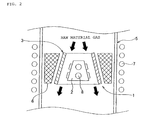
- FIG. 2 is a schematic view showing the neighborhood of a reaction chamber of the epitaxial growth unit that uses a susceptor shown in Fig. 1.
- a susceptor 1 according to the first embodiment is disposed at a center portion of the reaction chamber 5 and a heat insulating material 6 is disposed along an outer periphery portion of the susceptor 1.
- a high frequency coil 7 is spirally disposed.
- the susceptor 1 has a disposition configuration where, a direction of the external member of Fig. 1(b) is disposed upside down and inside thereof the susceptor according to Fig. 1(a) is disposed covered therewith. Trapezoidal planes of the internal susceptor 2 and trapezoidal planes of the external member 3 are disposed adjusted so as to be in parallel or substantially parallel.
- the heat insulating material 6 is disposed between an inner wall of the reaction chamber 5 and the external periphery of the susceptor 1 to inhibit the heat from being released.
- the high frequency coil 7 applies a high frequency to the susceptor 1 made of graphite to allow the susceptor 1 generating heat.
- Fig. 2 epitaxial growth by use of the susceptor according to the first embodiment will be described with reference to Fig. 2.
- substrates 8 are placed to carry out epitaxial growth.
- the internal susceptor 2 is disposed at a position shown in Fig. 2 and the high frequency coil 7 is operated to heat the susceptor to a temperature appropriate to carry out the epitaxial growth.
- a reaction gas is supplied flowing between the internal susceptor 2 of the susceptor 1 and the external member 3 thereof (arrow marks in Fig. 2).
- the susceptor according to the first embodiment since the susceptor according to the first embodiment is employed in a semiconductor epitaxial growth process, the respective substrate temperatures can be made constant and a plurality of epitaxial films high in the uniformity can be simultaneously obtained. Furthermore, when polycrystalline silicon carbide or polycrystalline tantalum carbide is used to cover, impurities contained in the susceptor made of graphite can be inhibited from being emitted. In particular, when the polycrystalline tantalum carbide is used to cover, since the tantalum carbide is a material that is excellent in the high temperature characteristics and excellent as well in the corrosion resistance to hydrogen, a coating material can be inhibited from sublimating and graphite can be inhibited from being exposed, and thereby the impurity can be inhibited from being emitted.
- the internal susceptor 2 and/or external member 3 may be used as a heater. Furthermore, as a modification example of an arrangement inside of the reaction chamber 5, as shown in Fig. 3, the susceptor 1 and heat insulating material 6 of Fig. 2 may be disposed upside down. At this time, a reaction gas is flowed from bottom up (arrow marks in Fig. 3).
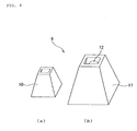
- FIG. 4 is a perspective view separately showing constituent articles of a susceptor involving a second embodiment of the invention, (a) showing an internal member, and (b) showing a barrel type external susceptor.
- a susceptor 9 shown in Fig. 2 includes an internal member 10 with graphite as a base material and an external susceptor 11 with graphite as a base material. Surfaces thereof are preferably covered with polycrystalline silicon carbide or polycrystalline tantalum carbide.
- the external susceptor 11 four trapezoidal planes (all four trapezoidal planes have the same area) each having a counter boring portion 12 are tilted to a perpendicular at a predetermined angle and hypotenuses thereof are bonded each other, and thereby the external susceptor 11 is formed.
- the internal member 10 has a substantially similar shape as the external susceptor 11 and can be disposed inside the external susceptor 11.
- the internal member 10 has four trapezoidal planes (all four trapezoidal planes have the same area), each of which, when the internal member 10 is disposed inside the external susceptor 11, can be oppositely disposed in parallel or in substantially parallel to each of the trapezoidal planes having a counter boring portion 12 of the external susceptor 11. That is, each of the trapezoidal planes of the internal member 10 is tilted to a perpendicular at a predetermined angle.
- a tilt angle of each of the trapezoidal planes of the internal member 10 is, to a perpendicular direction, preferably in the range of 2 to 45° and a tilt angle of each of the trapezoidal planes of the external susceptor 11 is, to a perpendicular direction, preferably in the range of 2 to 45°.
- a flow path on an inlet side of a gas is preferably made wide and a flow path on an outlet side is preferably made narrow.
- a tilt angle of the trapezoidal planes of the internal susceptor 2 is set at 12° to a perpendicular direction and a tilt angle of the trapezoidal planes of the external member 3 is set at 8° to a perpendicular direction.
- a distance between planes of the internal susceptor 2 and the external member 3 is in the range of 5 to 60 mm and desirably in the range of 10 to 25 mm.
- the counter boring portion 12 may be disposed at least one. Still furthermore, the number of the trapezoidal planes of the internal susceptor 2 and the external member 3, without restricting to four, may be three or more, respectively.
- the susceptor 9 involving the embodiment can be applied in place of the susceptor 1 inside of the reaction chamber 5 of the epitaxial growth unit in Fig. 2. Thereby, advantages similar to that of the first embodiment can be obtained. Furthermore, as a modification example of the embodiment, the internal member 10 and/or external susceptor 11 may be used as a heater.
- a susceptor 13 where the internal susceptor 2 of Fig. 1 and the external susceptor 11 of Fig. 2 are applied may be constituted.
- the susceptor 13 can be applied in place of the susceptor 1 inside of the reaction chamber 5 of the epitaxial growth unit in Fig. 2.
- a pin when a substrate is placed in a gravity-defying direction, a pin may be used to inhibit from falling.
- H 2 gas that is a carrier gas and Ar gas that is an inert gas were introduced from a raw material gas feed port (not shown in the drawing) and an inert gas feed port (not shown in the drawing) to maintain the inside of the reaction chamber at 100 Torr.
- the H 2 gas and Ar gas were continuously exhausted from an exhaust port (not shown in the drawing) and pressure inside of the reaction chamber is controlled with a pressure control valve (not shown in the drawing) disposed downstream of the exhaust port.
- a spiral high frequency induction coil 7 was turned on to heat the susceptor to 1350°C. At that time, as a temperature inside of a furnace, a temperature on a wafer was measured with a radiation thermometer. From 1350°C and upward, a slight amount of raw material gas was introduced from a feed port (not shown in the drawing) to suppress the silicon carbide wafer from damaging caused by the H 2 etching. In this case, as the raw material gas, SiH 4 and C 3 H 8 were used.
- the susceptor was used as a heating source and a heat insulating material was disposed, not only the heating efficiency was very good and thereby the power consumption could be saved, but also since a speedy temperature rise could be attained the damage owing to the H 2 etching during temperature rise of the wafer could be suppressed. As a result, high quality epitaxial layers could be obtained.
- the susceptor and wafer were heated to 1835°C that is high as an epitaxial growth temperature, followed by maintaining a temperature inside of the furnace constant. Since the wafer was directly heated with the susceptor as a heating source and the heat insulating material was disposed, the heating efficiency was largely improved; accordingly, a speedy temperature rise and epitaxial growth under high temperatures could be realized.
- a flow rate of SiH 4 and that of C 3 H 8 were increased to 120 sccm and 30 sccm, N 2 gas that is a doping gas was supplied at 0.05 sccm, and thereby the formation of the epitaxial layer was began.
- a growth temperature of 1835°C, growth pressure of 100 Torr, a C/Si ratio of 0.75, a SiH 4 /H 2 ratio of 0.4% by mole, a C 3 H 8 /H 2 ratio of 0.1% by mole and a growth time of 4 hr were adopted.
- the growth speed at that time was 33 ⁇ m/h and an epitaxial layer such thick as substantially 130 ⁇ m was obtained after 4 hr's growth.
- a surface state of a thick silicon carbide epitaxial layer was a mirror surface and a high quality layer having no large surface defect could be formed.
- distributions of film thicknesses and surface roughnesses (a) in a parallel direction with a gas flow and (b) in an orthogonal direction to a gas flow of an epitaxial layer of silicon carbide are shown.
- edge portion are excluded, excellent uniformity of ⁇ /m of 2 to 4% was obtained. This is because, owing to the use of the susceptor as a heating source and the disposition of the insulating material, the temperature uniformity of the wafers was improved.
- the RMS in Fig. 6 means root mean square roughness and this is same in the following.
- the growth speed increased in proportion to the SiH 4 flow rate and a growth speed such high as 44 ⁇ m/h was obtained.
- the susceptor was a heating source, a raw material gas contributing to a reaction in the neighborhood of a wafer was efficiently heated and decomposed.
- a smooth surface state of 0.3 nm was obtained.
- the RMS here was obtained of a range of 10 ⁇ 10 ⁇ m 2 .
- the invention can be modified in the design within a range that does not deviate from a range of claims and is not restricted to the embodiments and examples.
Landscapes
- Chemical & Material Sciences (AREA)
- Engineering & Computer Science (AREA)
- Materials Engineering (AREA)
- Metallurgy (AREA)
- Organic Chemistry (AREA)
- General Chemical & Material Sciences (AREA)
- Chemical Kinetics & Catalysis (AREA)
- Crystallography & Structural Chemistry (AREA)
- Mechanical Engineering (AREA)
- Chemical Vapour Deposition (AREA)
- Container, Conveyance, Adherence, Positioning, Of Wafer (AREA)
- Crystals, And After-Treatments Of Crystals (AREA)
Applications Claiming Priority (2)
| Application Number | Priority Date | Filing Date | Title |
|---|---|---|---|
| JP2004106950A JP4551106B2 (ja) | 2004-03-31 | 2004-03-31 | サセプタ |
| PCT/JP2005/005675 WO2005096356A1 (ja) | 2004-03-31 | 2005-03-28 | サセプタ |
Publications (2)
| Publication Number | Publication Date |
|---|---|
| EP1732111A1 true EP1732111A1 (de) | 2006-12-13 |
| EP1732111A4 EP1732111A4 (de) | 2009-11-04 |
Family
ID=35064063
Family Applications (1)
| Application Number | Title | Priority Date | Filing Date |
|---|---|---|---|
| EP05721602A Withdrawn EP1732111A4 (de) | 2004-03-31 | 2005-03-28 | Suszeptor |
Country Status (8)
| Country | Link |
|---|---|
| US (1) | US20070186858A1 (de) |
| EP (1) | EP1732111A4 (de) |
| JP (1) | JP4551106B2 (de) |
| KR (1) | KR101030422B1 (de) |
| CN (1) | CN100468631C (de) |
| CA (1) | CA2558591A1 (de) |
| TW (1) | TW200537602A (de) |
| WO (1) | WO2005096356A1 (de) |
Cited By (1)
| Publication number | Priority date | Publication date | Assignee | Title |
|---|---|---|---|---|
| US8404049B2 (en) | 2007-12-27 | 2013-03-26 | Memc Electronic Materials, Inc. | Epitaxial barrel susceptor having improved thickness uniformity |
Families Citing this family (10)
| Publication number | Priority date | Publication date | Assignee | Title |
|---|---|---|---|---|
| JP4551106B2 (ja) * | 2004-03-31 | 2010-09-22 | 東洋炭素株式会社 | サセプタ |
| US20080314319A1 (en) * | 2007-06-19 | 2008-12-25 | Memc Electronic Materials, Inc. | Susceptor for improving throughput and reducing wafer damage |
| CN102312198B (zh) * | 2010-06-30 | 2013-08-21 | 上方能源技术(杭州)有限公司 | 一种蒸镀源及蒸镀镀膜装置 |
| CN102560434B (zh) * | 2010-12-13 | 2014-10-22 | 北京北方微电子基地设备工艺研究中心有限责任公司 | 金属有机化合物化学气相沉积设备 |
| JP2013055201A (ja) * | 2011-09-02 | 2013-03-21 | Tokyo Electron Ltd | 熱処理装置 |
| JP5880297B2 (ja) * | 2012-06-07 | 2016-03-08 | 三菱電機株式会社 | 基板支持体、半導体製造装置 |
| KR101431606B1 (ko) * | 2014-02-24 | 2014-08-22 | (주)앤피에스 | 기판 처리 장치 |
| CN106337204B (zh) * | 2015-07-17 | 2018-11-06 | 中国科学院苏州纳米技术与纳米仿生研究所 | 石墨托以及装有石墨托的晶体生长炉 |
| JP7247749B2 (ja) * | 2019-05-27 | 2023-03-29 | 住友金属鉱山株式会社 | 炭化ケイ素多結晶膜の成膜方法、サセプタ、及び、成膜装置 |
| CN119877089B (zh) * | 2025-03-27 | 2025-06-20 | 浙江丽水中欣晶圆半导体科技有限公司 | 一种重掺磷衬底高阻值外延片生产设备 |
Family Cites Families (14)
| Publication number | Priority date | Publication date | Assignee | Title |
|---|---|---|---|---|
| US4099041A (en) * | 1977-04-11 | 1978-07-04 | Rca Corporation | Susceptor for heating semiconductor substrates |
| JPH0773099B2 (ja) * | 1986-07-28 | 1995-08-02 | 古河電気工業株式会社 | 半導体気相成長装置 |
| JPH01125923A (ja) * | 1987-11-11 | 1989-05-18 | Sumitomo Chem Co Ltd | 気相成長装置 |
| JP2849642B2 (ja) * | 1989-09-26 | 1999-01-20 | 豊田合成株式会社 | 化合物半導体の気相成長装置 |
| JPH03131017A (ja) * | 1989-10-17 | 1991-06-04 | Fujitsu Ltd | 気相成長装置 |
| US5104690A (en) * | 1990-06-06 | 1992-04-14 | Spire Corporation | CVD thin film compounds |
| JPH04241415A (ja) * | 1991-01-14 | 1992-08-28 | Furukawa Electric Co Ltd:The | 気相成長装置 |
| JPH06188195A (ja) * | 1992-12-16 | 1994-07-08 | Sumitomo Chem Co Ltd | 気相成長装置 |
| US6217662B1 (en) | 1997-03-24 | 2001-04-17 | Cree, Inc. | Susceptor designs for silicon carbide thin films |
| JPH11157989A (ja) * | 1997-11-25 | 1999-06-15 | Toyo Tanso Kk | 気相成長用サセプター及びその製造方法 |
| JPH11176757A (ja) * | 1997-12-11 | 1999-07-02 | Shimada Phys & Chem Ind Co Ltd | バレル型気相成長装置 |
| IL125690A0 (en) * | 1998-08-06 | 1999-04-11 | Reiser Raphael Joshua | Furnace for processing semiconductor wafers |
| JP3659564B2 (ja) * | 1999-10-26 | 2005-06-15 | 財団法人電力中央研究所 | 半導体結晶の製造方法およびこれを利用する製造装置 |
| JP4551106B2 (ja) * | 2004-03-31 | 2010-09-22 | 東洋炭素株式会社 | サセプタ |
-
2004
- 2004-03-31 JP JP2004106950A patent/JP4551106B2/ja not_active Expired - Fee Related
-
2005
- 2005-03-28 WO PCT/JP2005/005675 patent/WO2005096356A1/ja not_active Ceased
- 2005-03-28 EP EP05721602A patent/EP1732111A4/de not_active Withdrawn
- 2005-03-28 CA CA002558591A patent/CA2558591A1/en not_active Abandoned
- 2005-03-28 KR KR1020067019984A patent/KR101030422B1/ko not_active Expired - Fee Related
- 2005-03-28 CN CNB2005800103596A patent/CN100468631C/zh not_active Expired - Fee Related
- 2005-03-28 US US10/594,562 patent/US20070186858A1/en not_active Abandoned
- 2005-03-30 TW TW094110103A patent/TW200537602A/zh not_active IP Right Cessation
Cited By (1)
| Publication number | Priority date | Publication date | Assignee | Title |
|---|---|---|---|---|
| US8404049B2 (en) | 2007-12-27 | 2013-03-26 | Memc Electronic Materials, Inc. | Epitaxial barrel susceptor having improved thickness uniformity |
Also Published As
| Publication number | Publication date |
|---|---|
| KR101030422B1 (ko) | 2011-04-20 |
| KR20060131921A (ko) | 2006-12-20 |
| JP4551106B2 (ja) | 2010-09-22 |
| CN100468631C (zh) | 2009-03-11 |
| WO2005096356A1 (ja) | 2005-10-13 |
| US20070186858A1 (en) | 2007-08-16 |
| CN1938822A (zh) | 2007-03-28 |
| JP2005294508A (ja) | 2005-10-20 |
| EP1732111A4 (de) | 2009-11-04 |
| TW200537602A (en) | 2005-11-16 |
| TWI376730B (de) | 2012-11-11 |
| CA2558591A1 (en) | 2005-10-13 |
Similar Documents
| Publication | Publication Date | Title |
|---|---|---|
| KR101201589B1 (ko) | 고성능 화합물 반도체 물질을 제조하기 위한 증착기술 | |
| EP0970267B1 (de) | Suszeptor ausführungen für siliziumkarbid-dünnschichten | |
| US9123759B2 (en) | Susceptor, vapor phase growth apparatus, and method of manufacturing epitaxial wafer | |
| JP3845563B2 (ja) | 炭化珪素膜のcvd方法、cvd装置及びcvd装置用サセプター | |
| US20110259879A1 (en) | Multi-Zone Induction Heating for Improved Temperature Uniformity in MOCVD and HVPE Chambers | |
| US20080173239A1 (en) | Method, system, and apparatus for the growth of SiC and related or similar material, by chemical vapor deposition, using precursors in modified cold-wall reactor | |
| US8328943B2 (en) | Film forming apparatus and method | |
| EP2549522A1 (de) | Herstellungsverfahren für halbleiterdünnschichten, vorrichtung zur herstellung von halbleiterdünnschichten, suszeptor und suszeptorenwerkzeug | |
| WO2005093137A1 (en) | Reduction of carrot defects in silicon carbide epitaxy | |
| US20140339684A1 (en) | Synthetic diamond coated compound semiconductor substrates | |
| JP7419779B2 (ja) | サセプタ及び化学気相成長装置 | |
| WO2005028701A2 (en) | Methods and apparatus for controlling formation of deposits in a deposition system and deposition systems and methods including the same | |
| EP1732111A1 (de) | Suszeptor | |
| US12492488B2 (en) | Silicon carbide epitaxial growth device and method of manufacturing silicon carbide epitaxial wafer | |
| US7901508B2 (en) | Method, system, and apparatus for the growth of SiC and related or similar material, by chemical vapor deposition, using precursors in modified cold-wall reactor | |
| US20160240369A1 (en) | Method for manufacturing compound semiconductor epitaxial substrates including heating of carrier gas | |
| JP2023024445A (ja) | SiCデバイス及びSiCデバイスの製造方法 | |
| JP2023023081A (ja) | SiCエピタキシャルウェハ及びSiCエピタキシャルウェハの製造方法 | |
| KR101088678B1 (ko) | 박막 형성 방법 | |
| KR101916226B1 (ko) | 증착 장치 및 증착 방법 | |
| JP7296914B2 (ja) | サテライトおよび炭化珪素半導体装置の製造方法 | |
| JP2025078071A (ja) | SiCエピタキシャルウェハ | |
| KR20130077488A (ko) | 탄화규소 증착 방법 | |
| Schöner | New development in hot wall vapor phase epitaxial growth of silicon carbide | |
| CN119101987A (zh) | 衬底外延生长装置、预热环及其制作方法 |
Legal Events
| Date | Code | Title | Description |
|---|---|---|---|
| PUAI | Public reference made under article 153(3) epc to a published international application that has entered the european phase |
Free format text: ORIGINAL CODE: 0009012 |
|
| 17P | Request for examination filed |
Effective date: 20060907 |
|
| AK | Designated contracting states |
Kind code of ref document: A1 Designated state(s): AT BE BG CH CY CZ DE DK EE ES FI FR GB GR HU IE IS IT LI LT LU MC NL PL PT RO SE SI SK TR |
|
| DAX | Request for extension of the european patent (deleted) | ||
| A4 | Supplementary search report drawn up and despatched |
Effective date: 20091006 |
|
| 17Q | First examination report despatched |
Effective date: 20110608 |
|
| GRAP | Despatch of communication of intention to grant a patent |
Free format text: ORIGINAL CODE: EPIDOSNIGR1 |
|
| RIC1 | Information provided on ipc code assigned before grant |
Ipc: C30B 31/14 20060101ALI20130301BHEP Ipc: C23C 16/458 20060101ALI20130301BHEP Ipc: H01L 21/687 20060101ALI20130301BHEP Ipc: H01L 21/67 20060101ALI20130301BHEP Ipc: C30B 25/12 20060101AFI20130301BHEP |
|
| STAA | Information on the status of an ep patent application or granted ep patent |
Free format text: STATUS: THE APPLICATION IS DEEMED TO BE WITHDRAWN |
|
| 18D | Application deemed to be withdrawn |
Effective date: 20130801 |