EP1733461B1 - Vcsel oder led mit geneigtem resonator ohne wellenleitung - Google Patents
Vcsel oder led mit geneigtem resonator ohne wellenleitung Download PDFInfo
- Publication number
- EP1733461B1 EP1733461B1 EP05728328A EP05728328A EP1733461B1 EP 1733461 B1 EP1733461 B1 EP 1733461B1 EP 05728328 A EP05728328 A EP 05728328A EP 05728328 A EP05728328 A EP 05728328A EP 1733461 B1 EP1733461 B1 EP 1733461B1
- Authority
- EP
- European Patent Office
- Prior art keywords
- cavity
- optoelectronic device
- resonant
- tilted
- light
- Prior art date
- Legal status (The legal status is an assumption and is not a legal conclusion. Google has not performed a legal analysis and makes no representation as to the accuracy of the status listed.)
- Expired - Lifetime
Links
Images





Classifications
-
- H—ELECTRICITY
- H01—ELECTRIC ELEMENTS
- H01S—DEVICES USING THE PROCESS OF LIGHT AMPLIFICATION BY STIMULATED EMISSION OF RADIATION [LASER] TO AMPLIFY OR GENERATE LIGHT; DEVICES USING STIMULATED EMISSION OF ELECTROMAGNETIC RADIATION IN WAVE RANGES OTHER THAN OPTICAL
- H01S5/00—Semiconductor lasers
- H01S5/10—Construction or shape of the optical resonator, e.g. extended or external cavity, coupled cavities, bent-guide, varying width, thickness or composition of the active region
- H01S5/18—Surface-emitting [SE] lasers, e.g. having both horizontal and vertical cavities
- H01S5/183—Surface-emitting [SE] lasers, e.g. having both horizontal and vertical cavities having only vertical cavities, e.g. vertical cavity surface-emitting lasers [VCSEL]
-
- B—PERFORMING OPERATIONS; TRANSPORTING
- B82—NANOTECHNOLOGY
- B82Y—SPECIFIC USES OR APPLICATIONS OF NANOSTRUCTURES; MEASUREMENT OR ANALYSIS OF NANOSTRUCTURES; MANUFACTURE OR TREATMENT OF NANOSTRUCTURES
- B82Y20/00—Nanooptics, e.g. quantum optics or photonic crystals
-
- H—ELECTRICITY
- H10—SEMICONDUCTOR DEVICES; ELECTRIC SOLID-STATE DEVICES NOT OTHERWISE PROVIDED FOR
- H10H—INORGANIC LIGHT-EMITTING SEMICONDUCTOR DEVICES HAVING POTENTIAL BARRIERS
- H10H20/00—Individual inorganic light-emitting semiconductor devices having potential barriers, e.g. light-emitting diodes [LED]
- H10H20/80—Constructional details
- H10H20/81—Bodies
- H10H20/814—Bodies having reflecting means, e.g. semiconductor Bragg reflectors
- H10H20/8142—Bodies having reflecting means, e.g. semiconductor Bragg reflectors forming resonant cavity structures
-
- H—ELECTRICITY
- H01—ELECTRIC ELEMENTS
- H01S—DEVICES USING THE PROCESS OF LIGHT AMPLIFICATION BY STIMULATED EMISSION OF RADIATION [LASER] TO AMPLIFY OR GENERATE LIGHT; DEVICES USING STIMULATED EMISSION OF ELECTROMAGNETIC RADIATION IN WAVE RANGES OTHER THAN OPTICAL
- H01S2301/00—Functional characteristics
- H01S2301/02—ASE (amplified spontaneous emission), noise; Reduction thereof
-
- H—ELECTRICITY
- H01—ELECTRIC ELEMENTS
- H01S—DEVICES USING THE PROCESS OF LIGHT AMPLIFICATION BY STIMULATED EMISSION OF RADIATION [LASER] TO AMPLIFY OR GENERATE LIGHT; DEVICES USING STIMULATED EMISSION OF ELECTROMAGNETIC RADIATION IN WAVE RANGES OTHER THAN OPTICAL
- H01S5/00—Semiconductor lasers
- H01S5/20—Structure or shape of the semiconductor body to guide the optical wave ; Confining structures perpendicular to the optical axis, e.g. index or gain guiding, stripe geometry, broad area lasers, gain tailoring, transverse or lateral reflectors, special cladding structures, MQW barrier reflection layers
- H01S5/2004—Confining in the direction perpendicular to the layer structure
- H01S5/2018—Optical confinement, e.g. absorbing-, reflecting- or waveguide-layers
- H01S5/2027—Reflecting region or layer, parallel to the active layer, e.g. to modify propagation of the mode in the laser or to influence transverse modes
-
- H—ELECTRICITY
- H01—ELECTRIC ELEMENTS
- H01S—DEVICES USING THE PROCESS OF LIGHT AMPLIFICATION BY STIMULATED EMISSION OF RADIATION [LASER] TO AMPLIFY OR GENERATE LIGHT; DEVICES USING STIMULATED EMISSION OF ELECTROMAGNETIC RADIATION IN WAVE RANGES OTHER THAN OPTICAL
- H01S5/00—Semiconductor lasers
- H01S5/20—Structure or shape of the semiconductor body to guide the optical wave ; Confining structures perpendicular to the optical axis, e.g. index or gain guiding, stripe geometry, broad area lasers, gain tailoring, transverse or lateral reflectors, special cladding structures, MQW barrier reflection layers
- H01S5/205—Antiguided structures
-
- H—ELECTRICITY
- H01—ELECTRIC ELEMENTS
- H01S—DEVICES USING THE PROCESS OF LIGHT AMPLIFICATION BY STIMULATED EMISSION OF RADIATION [LASER] TO AMPLIFY OR GENERATE LIGHT; DEVICES USING STIMULATED EMISSION OF ELECTROMAGNETIC RADIATION IN WAVE RANGES OTHER THAN OPTICAL
- H01S5/00—Semiconductor lasers
- H01S5/30—Structure or shape of the active region; Materials used for the active region
- H01S5/34—Structure or shape of the active region; Materials used for the active region comprising quantum well or superlattice structures, e.g. single quantum well [SQW] lasers, multiple quantum well [MQW] lasers or graded index separate confinement heterostructure [GRINSCH] lasers
Definitions
- the invention pertains to the field of optoelectronic devices. More particularly, the invention pertains to edge-emitting lasers, surface emitting lasers, wavelength-tunable lasers, optical amplifiers, photodetectors, optical switches, and light-emitting diodes.
- a tilted cavity semiconductor laser includes at least one active element with an active region generating an optical gain by injection of a current and mirrors.
- the active element is placed into a cavity.
- the cavity is designed such that the optical path of the resonant optical mode is tilted with respect to both the vertical direction and the lateral plane.
- the feedback both in the vertical and in the lateral direction is provided for the resonant optical mode.
- the laser operates as both a surface emitting laser and an edge-emitting laser
- Employing a tilted optical mode allows the use of substantially fewer layers in the bottom and the top interference reflectors than in conventional lasers. This preserves the necessary high reflection coefficients.
- a wavelength-stabilized laser is realized for edge-emitters. The wavelength stabilization is due to the difference in the dispersion laws for the tilted optical modes in layers having different refractive indices.
- FIG. 1(a) A prior art semiconductor diode laser, or more specifically, an edge-emitting laser, is shown in Fig. 1(a) .
- the laser structure (100) is grown epitaxially on an n-doped substrate (101).
- the structure further includes an n-doped cladding layer (102), a waveguide (103), a p-doped cladding layer (108), and a p-contact layer (109).
- the waveguide (103) includes an n-doped part (104), a confinement layer (105) with an active region (106) inside the confinement layer, and a p-doped part (107).
- the n-contact (111) is contiguous with the substrate (101), and a p-contact (112) is mounted on the p-contact layer (109).
- the active region (106) generates light when a forward bias (113) is applied.
- the profile of the optical mode in the vertical direction (z) is determined by the refractive index profile in the z-direction.
- the waveguide (103) is bounded in the lateral plane by a front facet (116) and a rear facet (117). If a special highly reflecting coating is put on the rear facet (117), the laser light (115) is emitted only through the front facet (116).
- the substrate (101) is preferably formed from any III-V semiconductor material or III-V semiconductor alloy, e.g. GaAs, InP, or GaSb. GaAs or InP are generally used depending on the desired emitted wavelength of laser radiation.
- the substrate (101) is preferably either a slice of a bulk crystal or an epilayer deposited on the slice of a bulk crystal.
- sapphire, SiC or Si (111) can be used as substrates for GaN-based lasers, i.e. laser structures the layers of which are formed of GaN, AlN, InN, or alloys of these materials.
- the substrate (101) is doped by an n-type, or donor impurity.
- Possible donor impurities include, but are not limited to S, Se, Te, and amphoteric impurities like Si, Ge, or Sn where the latter are introduced under such technological conditions that they are incorporated predominantly into the cation sublattice and serve as donor impurities.
- the n-doped cladding layer (102) is preferably formed from a material lattice-matched or nearly lattice-matched to the substrate (101), is transparent to the generated light, and is doped by a donor impurity.
- the n-doped cladding layer is preferably formed from a GaAlAs alloy or an In(Ga,Al)P alloy lattice matched or nearly lattice matched to a GaAs substrate.
- the n-doped part (104) of the waveguide (103) is preferably formed from a material lattice-matched or nearly lattice-matched to the substrate (101), is transparent to the generated light and is doped by a donor impurity.
- the n-doped part (104) of the waveguide is preferably formed of a GaAlAs alloy having an Al content lower than that in the n-doped cladding layer (102), or of GaAs.
- the p-doped part (107) of the waveguide (103) is preferably formed from a material lattice-matched or nearly lattice-matched to the substrate (101), is transparent to the generated light and is doped by an acceptor impurity.
- the p-doped part (107) of the waveguide is formed from the same material as the n-doped part (104), but doped by an acceptor impurity.
- acceptor impurities include, but are not limited to, Be, Mg, Zn, Cd, Pb, Mn and amphoteric impurities like Si, Ge, or Sn where the latter are introduced under such technological conditions that they are incorporated predominantly into the anion sublattice and serve as acceptor impurities.
- the p-doped cladding layer (108) is preferably formed from a material lattice-matched or nearly lattice-matched to the substrate (101), is transparent to the generated light, and is doped by an acceptor impurity.
- the p-doped cladding layer (108) is formed from the same material as the n-doped cladding layer (102), but is doped by an acceptor impurity.
- the p-contact layer (109) is preferably formed from a material lattice-matched or nearly lattice matched to the substrate, is transparent to the generated light and is doped by an acceptor impurity.
- the doping level is preferably higher than that in the p-cladding layer (108).
- the metal contacts (111) and (112) are preferably formed from multi-layered metal structures.
- the metal contact (111) is preferably formed from the structures including, but not limited to, the structure Ni-Au-Ge.
- Metal contacts (112) are preferably formed from structures including, but not limited to, the structure Ti-Pt-Au.
- the confinement layer (105) is preferably formed from a material lattice-matched or nearly lattice-matched to the substrate (101), is transparent to the generated light, and is undoped or weakly doped.
- the confinement layers are preferably formed from the same material as the substrate (101).
- the active region (106) placed within the confinement layer (105) is preferably formed by any insertion, the energy band gap of which is narrower than that of the substrate (101).
- Possible active regions (106) include, but are not limited to, a single-layer or a multi-layer system of quantum wells, quantum wires, quantum dots, or any combination thereof.
- examples of the active region (106) include, but are not limited to, a system of insertions of InAs, In 1-x Ga x As, In x Ga 1-x-y Al y As, In x Ga 1-x As 1-y N y or similar materials.
- One of the major shortcomings of the edge-emitting laser is a variation of the energy band gap with temperature resulting in an undesirable temperature dependence of the wavelength of emitted light, particularly for high output power operation.
- Fig. 1(b) shows schematically a prior art surface emitting laser, particularly, a vertical cavity surface emitting laser (VCSEL) (120).
- the active region (126) is put into a cavity (123), which is sandwiched between an n-doped bottom mirror (122) and a p-doped top mirror (128).
- the cavity (123) includes an n-doped layer (124), a confinement layer (125), and a p-doped layer (127).
- Bragg reflectors each including a periodic sequence of alternating layers having low and high refractive indices are used as a bottom mirror (122) and a top mirror (128).
- the active region (126) generates light when a forward bias (113) is applied. Light comes out (135) through the optical aperture (132).
- the wavelength of the emitted laser light from the VCSEL is determined by the length of the cavity (123).
- the layers forming the bottom mirror (122) are preferably formed from materials lattice-matched or nearly lattice matched to the substrate (101), are transparent to the generated light, are doped by a donor impurity and have alternating high and low refractive indices.
- alternating layers of GaAs and GaAlAs or layers of GaAlAs having alternating aluminum content preferably form the mirror.
- the n-doped part (124) of the cavity (123) is preferably formed from a material lattice-matched or nearly lattice-matched to the substrate (101), is transparent to the generated light and is doped by a donor impurity.
- the p-doped part (127) of the cavity (123) is preferably formed from a material lattice-matched or nearly lattice-matched to the substrate (101), is transparent to the generated light and is doped by an acceptor impurity.
- the layers forming the top mirror (128) are preferably formed from materials lattice-matched or nearly lattice-matched to the substrate (101), are transparent to the generated light, are doped by an acceptor impurity and have alternating high and low refractive indices.
- alternating layers of GaAs and GaAlAs or layers of GaAlAs having alternating aluminum content preferably form the mirror.
- the p-contact layer (129) is preferably formed from a material doped by an acceptor impurity.
- the preferred material is GaAs.
- the doping level is preferably higher than that in the top mirror (128).
- the p-contact layer (129) and the metal p-contact (112) are etched to form an optical aperture (132).
- the doping profile is optimized to reach a possibly low resistance of the device.
- the confinement layer (125) is preferably formed from a material lattice-matched or nearly lattice-matched to the substrate (101), is transparent to the generated light, and is undoped or weakly doped.
- the confinement layers are preferably formed from the same material as the substrate (101).
- the active region (126) placed within the confinement layer (125) is preferably formed by any insertion, the energy band gap of which is narrower than that of the substrate (101).
- Possible active regions (126) include, but are not limited to, a single-layer or a multi-layer system of quantum wells, quantum wires, quantum dots, or any combination thereof.
- examples of the active region (126) include, but are not limited to, a system of insertions of InAs, In 1-x Ga x As, In x Ga 1-x-y Al y As, In x Ga 1-x As 1-y N y or similar materials.
- the active region (126) generates optical gain when a forward bias (113) is applied.
- the active region (126) then emits light which is bounced between the bottom mirror (122) and the top mirror (128).
- the mirrors have high reflectivity for light propagating in the direction normal to the p-n junction plane, and the reflectivity of the bottom mirror (122) is preferably higher than that of the top mirror (128).
- the VCSEL design provides a positive feedback for light propagating in the vertical direction and finally results in lasing.
- the laser light (135) comes out through the optical aperture (132).
- a VCSEL temperature stabilization of the wavelength. Temperature variations of the wavelength follow the temperature variations of the refractive index, which is an order of magnitude smaller than the variations of the semiconductor band gap energy.
- One severe disadvantage of a VCSEL is that its output power is limited by a few mW, as it is not possible to provide efficient heat dissipation in the VCSEL geometry.
- the invention discloses a semiconductor optoelectronic device including at least one cavity and one multilayered interference reflector.
- the cavity is designed preferably to possess properties of an antiwaveguiding cavity, where no optical modes having a significant overlap with the active medium propagate in the lateral plane.
- the existing optical modes are the modes propagating in the vertical direction or in a direction tilted to the vertical direction, such that the tilt angle is smaller than the angle of the total internal reflection at the semiconductor-air interface and light in such optical modes comes out of the device through the top surface or the substrate.
- This design reduces the influence of parasitic optical modes and improves characteristics of optoelectronic devices including, but not limited to, vertical cavity surface emitting lasers, tilted cavity lasers emitting through the top surface or a substrate, vertical or tilted cavity resonant photodetectors, vertical or tilted cavity resonant optical amplifiers, and light-emitting diodes.
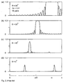
- Figs. 2(a) through 2(d) illustrate the reflectivity spectrum of a periodic multilayered structure for a few different tilt angles (65°, 55°, 40°, and 0°, respectively) of the propagating TE electromagnetic wave, as disclosed by Yariv et al. ( A. Yariv, P. Yeh, "Optical Waves in Crystals. Propagation and Control of Laser Radiation", Wiley 1984 ).
- the reflectivity is plotted as a function of the frequency ⁇ of the electromagnetic wave, and ⁇ is measured in units of c / ⁇ , where c is the velocity of light in the vacuum.
- i spikes shifts towards higher frequencies, i.e., towards shorter wavelengths
- ii the amplitudes of the spikes increases
- iii the spikes become broader, forming stopbands with a reflectivity close to 1.
- the tilted cavity laser (300) is grown epitaxially on an n-doped substrate (101) and includes an n-doped bottom multilayered interference reflector (302), a cavity (303), a p-doped top multilayered interference reflector (308), and a p-contact layer (309).
- the cavity (303) includes an n-doped layer (304), a confinement layer (305), and a p-doped layer (307).
- the confinement layer (305) also includes an active region (306).
- the laser structure (300) is bounded in the lateral plane by a rear facet (317) and a front facet (316).
- the cavity (303) and the multilayered interference reflectors (302) and (307) are designed such that resonant conditions for the cavity and for the multilayered interference reflectors are met for only one tilted optical mode (320) propagating at a certain tilt angle and having a certain wavelength. If the rear facet (317) is covered by a highly reflecting coating, the output laser light (315) comes out only through the front facet (316).
- This tilted cavity laser is that wavelength stabilization and a high output power are obtained at the same time.
- the layers forming the bottom multilayered interference reflector (302) are preferably formed from materials lattice-matched or nearly lattice matched to the substrate (101), are transparent to the generated light, are doped by a donor impurity and have alternating high and low refractive indices.
- alternating layers of GaAs and GaAlAs or layers of GaAlAs having alternating aluminum content preferably form the mirror.
- the n-doped part (304) of the cavity (303) is preferably formed from a material lattice-matched or nearly lattice-matched to the substrate (101), is transparent to the generated light and is doped by a donor impurity.
- the p-doped part (307) of the cavity (303) is preferably formed from a material lattice-matched or nearly lattice-matched to the substrate (101), is transparent to the generated light and is doped by an acceptor impurity.
- the layers forming the top multilayered interference reflector (308) are preferably formed from materials lattice-matched or nearly lattice-matched to the substrate (101), are transparent to the generated light, are doped by an acceptor impurity and have alternating high and low refractive indices.
- alternating layers of GaAs and GaAlAs or layers of GaAlAs having alternating aluminium content preferably form the mirror.
- the p-contact layer (309) is preferably formed from a material doped by an acceptor impurity.
- the preferred material is GaAs.
- the doping level is preferably higher than that in the top multilayered interference reflector (308).
- the confinement layer (305) is preferably formed from a material lattice-matched or nearly lattice-matched to the substrate (101), is transparent to the generated light, and is undoped or weakly doped.
- the confinement layers are preferably formed from the same material as the substrate (101).
- the active region (306) placed within the confinement layer (305) is preferably formed by any insertion, the energy band gap of which is narrower than that of the substrate (101).
- Possible active regions (306) include, but are not limited to, a single-layer or a multi-layer system of quantum wells, quantum wires, quantum dots, or any combination thereof.
- examples of the active region (306) include, but are not limited to, a system of insertions of InAs, In 1-x Ga x As, In x Ga 1-x-y Al y As, In x Ga 1-x As 1-y N y or similar materials.
- Fig. 4(a) shows schematically a tilted cavity laser according to the U.S. Application Serial No. 10/943,044 filed September 16, 2004 , entitled “TILTED CAVITY SEMICONDUCTOR OPTOELECTRONIC DEVICE AND METHOD OF MAKING SAME", invented by the inventors of the present invention.
- the structure (400) includes a high-finesse cavity (410) and a multilayered interference reflector (MIR) (420).
- the high-finesse cavity (410) includes a layer (415) having a high refractive index sandwiched between a layer (412) and a layer (417) both having refractive indices lower than the refractive index of the layer (415).
- the reflectivity spectra of the high-finesse cavity (410) at a certain impinging angle ⁇ of light has a narrow dip.
- the finesse of the cavity defined as a ratio of the wavelength and the width of the dip is preferably larger than 5.
- the MIR (420) includes a structure of alternating layers (421) having a high refractive index and layers (422) having a low refractive index. Both the spectral position of the reflectivity dip of the cavity (410) and the stopband reflectivity maximum of the MIR (420) are functions of the angle ⁇ .
- This particular wavelength ⁇ 0 is the wavelength at which the tilted optical mode confined within the cavity (410) has the minimum leakage losses through the MIR (420). This promotes the selection of the tilted optical modes of a tilted cavity laser and ensures lasing at this wavelength ⁇ 0 .
- Fig. 4(b) shows schematically a structure (450) of a tilted cavity laser according to U.S. Application Serial No. 10/943,044 , where a high-finesse cavity (410) is sandwiched between a MIR (420) and a MIR (470).
- the selection of the tilted optical modes is based on the same principles as at the structure (400).
- Fig. 5(a) shows schematically the spatial profile of the resonant tilted optical mode in a tilted cavity laser according to U.S. Application Serial No. 10/943,044 .
- the tilted cavity laser is based on a GaAs/GaAlAs structure.
- the aluminum content is shown in Fig. 5(b) .
- Fig. 6 illustrates two possible designs of a vertical cavity surface emitting laser (VCSEL). The same figure also refers to two possible designs of a tilted cavity laser (TCL) where laser light comes out through the top mirror.
- VCSEL vertical cavity surface emitting laser
- TTL tilted cavity laser
- a conventional design (600) for a VCSEL shown in Fig. 6(a) , includes a bottom distributed Bragg reflector (DBR) (620), a cavity (610) including an active region (606), and a top DBR (630). Both the bottom DBR (620) and the top DBR (630) include a periodic structure of alternating layers (621) having a first refractive index, and layers (622) having a second refractive index. The second refractive index is lower than the first refractive index.
- the active region (606) is placed within the cavity (610), which is preferably formed of a material having a low refractive index. Light emission, below the lasing threshold, occurs in a plurality of optical modes which include both the modes propagating through the top mirror, and parasitic modes propagating along the waveguide or leaking into the substrate.
- the "resonant" cavity emission (for example at 1.3 ⁇ m) can be reflected by the DBR only for angles below ⁇ 5°.
- the long-wavelength edge of the stopband shifts to 1.27 ⁇ m and most of the 1.3 ⁇ m emission leaks into the substrate.
- the resonant optical mode of the device is illustrated in Fig. 6(a) as the dependence of the square of the electric field strength
- Fig. 6(b) shows a VCSEL (650) according to an embodiment of the present invention.
- a cavity (660) is formed of a material having a low refractive index.
- This structure is an antiwaveguiding structure.
- the active region is placed within a cavity having a low refractive index.
- Parasitic modes are suppressed. Tilted modes are partially or completely reflected (674) and only the modes, which come with very large angles with respect to the layer surface, penetrate into the active region and have weak overlap with the gain medium.
- only the modes (633) of the vertical resonator remain well defined and provide a high confinement factor.
- the resonant optical mode of the device is illustrated in Fig. 6(b) as the dependence of the square of the electric field strength
- One way to make a cavity antiwaveguiding is to provide a relationship between the refractive indices of a cavity and an averaged refractive index of a DBR: n cavity ⁇ n DBR , where the averaged refractive index of the DBR is defined as a square root of the weighted averaged square of the refractive index-
- a tilted cavity laser is designed such that it includes at least one cavity and at least one multilayered interference reflector (MIR) designed such that the refractive index of the cavity is lower than the effective refractive index of the MIR, which enables an efficient suppression of parasitic optical modes.
- MIR multilayered interference reflector
- Layers that compose the VCSEL (650) should obey the above-described relationship (Eq.(1)) between the refractive indices and are preferably lattice-matched or nearly lattice-matched to the substrate.
- the active medium realized as a single-layer or a multilayer structure of quantum wells, arrays of quantum wires, arrays of quantum dots or any combination thereof, may contain thin lattice mismatched layers.
- the entire structure of the device is grown on a metamorphic (plastically relaxed) buffer, lattice-mismatched to the substrate.
- the top DBR or the top MIR may be formed of either semiconductor or dielectric layers, or any combination thereof.
- a vertical or tilted cavity laser is designed such that the parasitic modes have large leaky losses to the substrate and the contact layers.
- the leaky losses are preferably higher than 10 cm -1 .
- a vertical or tilted cavity laser is designed such that the parasitic modes have a small confinement factor in the working p-n junction.
- the small confinement factor is preferably smaller than the confinement factor of the resonant optical mode by a factor larger than 3.
- the working p-n junction is the junction emitting light in lasers and optical amplifiers and the junction absorbing light in photodetectors.
- a vertical or a tilted cavity laser is designed such that the leaky losses to the substrate or to the contact layers for a first group of parasitic modes are preferably higher than 10 cm -1 .
- the confinement factor in the working p-n junction of the optical modes of a second group of parasitic modes are preferably smaller than the confinement factor of the resonant optical mode by a factor of 3.
- the Purcell effect reads that the probability of the radiative recombination for this resonance mode is increased by a number of times equal to the finesse of the cavity ( Q ), if the inhomogeneous broadening is smaller than the cavity dip width.
- Q quantum dot
- the Q-factor is estimated to be 1300 nm/0.1 nm, or approximately 13,000. This number corresponds to an average number of photon cycles in the cavity before escape. At low temperatures the homogeneous broadening in QD is very small (a few ⁇ eV) and the condition is fulfilled.
- the angle of the emission, where the enhancement is expected is very small and defined by the number of confined vertical modes in the cavity.
- the Purcell effect is measurable only in situations where the parasitic radiative modes are suppressed. This suppression is usually realized by etching of photonic crystal around the cavity, exhibiting a reflectivity stopband for lateral modes and confining the active vertical mode.
- the antiwaveguide structure of the present invention there may be no waveguiding modes. Moreover, no vertical resonant waveguide modes are possible for the emission with wavelength exceeding the resonant cavity wavelength. These states can be then effectively filled with fairly low radiative leakage.
- a tilted cavity laser is designed according to the present invention and includes an antiwaveguiding cavity, the tilted cavity laser has the same advantages as a VCSEL. Since there are no waveguiding optical modes having a significant overlap with the active medium, the number of the parasitic radiative channels is dramatically suppressed.
- this leakage does not contribute to making the gain medium transparent, as the leaking photons are not absorbed by the active media.
- the amount of the absorbed photons is negligible.
- the transparency regime may be reached with very small current (suppressed waste states and recycling of resonant photons).
- the gain anisotropy is defined by the quantum well or quantum dot symmetry and strain profile, and not by the cavity. Below threshold, light generated by the stimulated emission propagates and is amplified in all directions.
- the advantage of the VCSEL mode is low losses due to a highly-reflective DBR for a small portion (small angle) of light.
- a conventional VCSEL needs to be fully processed before it is proven that the wafer is good, and the device indeed generates laser light. If the same wafer is tested as a simple edge-emitter (stripe or four-side cleaved), it operates in a low-loss waveguide mode and surface lasing is not possible. In contrast, in the antiwaveguide VCSEL of the present invention, no waveguide modes are possible and vertical lasing may be realized and detected, e.g. as diffracted light at the facets and corners, from the scratched back side in vertical direction, etc. This dramatically reduces the time for evaluation and enables faster development loops.
- a tilted cavity laser which is designed to generate laser light in a resonant tilted optical mode.
- the laser light comes out in a vertical direction through the top mirror or through the bottom mirror to the substrate.
- a cavity having a low refractive index is sandwiched between two multilayered interference reflectors (MIR) having a high averaged refractive index.
- MIR multilayered interference reflectors
- Fig. 6(b) refers also to such tilted cavity lasers, but the cavity and the MIRs are designed such that a tilted optical mode characterized by a certain tilt angle is the resonant mode with the minimum leakage loss.
- Another embodiment of the present invention discloses a resonant photodetector, which operates in a vertical cavity geometry or in a tilted cavity geometry and includes a cavity exhibiting an antiwaveguiding effect.
- Fig. 9 shows schematically a photodetector (900) based on an antiwaveguiding cavity according to an embodiment of the present invention.
- the device (900) operates under a reverse bias (913).
- no light is absorbed at the p-n junction placed preferably in the layer (926) within the antiwaveguiding cavity (660)
- no current flows through the device.
- external light impinges on the top surface of the device at sufficiently small angles with respect to the normal direction (950)
- photons are absorbed within the p-n junction, generating electron-hole pairs. Electrons and holes are driven apart by an electric field creating a photocurrent.
- the photocurrent may be measured by a microampermeter (960).
- a novel feature of this photodetector is that only light in certain optical modes having a sufficient overlap with the p-n junction contribute to the photocurrent.
- the photodetector (900) is also selective in the direction of propagation of the incoming light and detects light propagating only from certain directions. This may be important for certain applications.
- a resonant cavity photodetector operates in combination with another optoelectronic device, where the latter generates light in an optical mode, which exists outside the device in the form of an evanescent electromagnetic field.
- the photodetector of the present invention is capable of detecting light in the near field zone of a light generating device.
- Yet another embodiment of the present invention discloses an optical amplifier, which operates in a vertical cavity geometry or in a tilted cavity geometry and includes an antiwaveguiding cavity.
- LED light emitting diode
- a vertical cavity surface emitting laser a tilted cavity laser, an optical amplifier, a photodetector, or a light-emitting device including an antiwaveguided cavity may be extended in various ways.
- the part of the MIR or the DBR close to the cavity has the weighted average refractive index according to Eq.(2) that satisfies Eq.(1).
- Eq.(2) the weighted average refractive index according to Eq.(2) that satisfies Eq.(1).
- the refractive index averaged over the entire MIR or DBR including additional remote layers will not necessarily satisfy Eq.(1).
- the refractive index of the cavity is preferably lower than the averaged refractive index of the part of the MIR or the DBR in the close vicinity of the cavity.
- new layers may be added such that a second, waveguiding cavity is formed, and parasitic optical modes propagating at large tilt angles to the vertical direction are possible.
- a necessary condition for the device to operate according to the present invention is that the overlap of such parasitic optical modes with the active medium is small.
- Further embodiments additionally include one or more of the following elements: contact layers, contacts, or oxide apertures as is well known in the art (e.g., Vertical-Cavity Surface-Emitting Lasers: Design, Fabrication, Characterization, and Applications by C.W. Wilmsen, H. Temkin, L.A. Coldren (editors), Cambridge University Press, 1999 ). Additionally deposited layers may be both semiconductor layers and dielectric layers or any combination thereof.
- the MIR or the DBR may be n-doped from the side of the n-contact.
- the MIR or the DBR may be p-doped from the side of the p-contact.
- the MIR or the DBR may be undoped or only weakly doped from one or both sides, and the contact is preferably realized as an intracavity contact.
- All additional elements like contact layers, contacts, oxide apertures, as well as various ways to apply a bias to a p-n junction, e.g. via doped DBRs or via intracavity contacts, where DBRs remain undoped or weakly doped, are well known in the art.
- the possible material combinations are known in the art for VCSELs (e.g., Vertical-Cavity Surface-Emitting Lasers: Design, Fabrication, Characterization, and Applications by C.W. Wilmsen, H. Temkin, L.A. Coldren (editors), Cambridge University Press, 1999 ). Similar elements and technological solutions are possible for tilted cavity lasers designed to emit light via the top surface or the substrate.
- optical amplifiers for both those designed to work as vertical cavity optical amplifiers and designed to work as tilted cavity optical amplifiers.
- resonant cavity photodetectors for both photodetectors designed to work as vertical cavity photodetectors and those designed to work as tilted cavity photodetectors.
- the present invention is also applicable to tunable vertical cavity surface emitting lasers (VCSELs) and tunable tilted cavity lasers, where the cavity includes both a light generating element and a modulator element.
- the modulator element includes a modulating layer, the refractive index of which can be tuned electronically due to a quantum confinement Stark effect or by the effect of bleaching. Tuning the refractive index within one layer within a cavity results in a shift of the wavelength of the emitted laser light (see N.N. Ledentsov and V.A. Shchukin, "WAVELENGTH-TUNABLE VERTICAL CAVITY SURFACE EMITTING LASER AND METHOD OF MAKING SAME", U.S. Patent No.
- ⁇ cavity n cavity ⁇ d cavity m ⁇ cos ⁇ cavity
- ⁇ cavity is the angle of propagation of a tilted mode within the cavity.
- the resonant optical mode is determined by the criterion that, at a certain angle of propagation of the optical mode, the resonant wavelength for the cavity coincides with the wavelength of the maximum reflectivity of the stopband of the MIR. This is a criterion of the phase matching between the cavity and the MIR. Let now the refractive index of the cavity be varied. Then the optical mode at a different wavelength no longer corresponds to the reflectivity stopband maximum of the MIR, and phase matching conditions are violated. If the stopband of the MIR is narrow, the phase matching conditions are of high importance as they insure low leakage losses of the optical mode.
- the phase matching conditions are no longer fulfilled and no lasing is possible. If the refractive index of the cavity is decreased, the phase matching conditions may be met at a different angle of propagation and a different wavelength and determine the shift of the wavelength of the resonant optical mode.
- the role of phase matching is not that important.
- the change of the resonant wavelength is determined mainly by the change of the refractive index of the cavity.
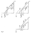
- ⁇ MIR vanishes at a smaller angle than ⁇ cavity , and the two curves, (704) for ⁇ cavity ( ⁇ ), and (705) for ⁇ MIR ( ⁇ ) behave as shown in Fig. 7(a) .
- the cavity in Fig. 7(a) has a higher refractive index than the MIR.
- the cavity and the MIR are designed such that the resonant mode is a tilted mode propagating in a direction tilted with respect to the direction normal to the lateral plane.
- the corresponding shift of the resonant wavelength depends on an interplay between two effects.
- the first effect is an average change of the refractive index of the cavity.
- the second effect is related to the matching conditions between adjacent layers forming the cavity, particularly, between the modulator and neighboring layers. The relative importance of these two effects depends on the relationship between the width of the stopband of the MIR at the normal incidence, ⁇ ⁇ stopband and the quantity, ⁇ MIR (0) - ⁇ 0 .
- the shift of the wavelength is mainly determined by the change of the average refractive index of the cavity, and phase-matching conditions do not play a role. If the average refractive index of the modulator increases, according to Eq.(7), the resonant wavelength also increases. In the case of a narrow stopband, ⁇ ⁇ ⁇ stopband ⁇ ⁇ MIR ( 0 ) - ⁇ 0 , the matching conditions begin to play an important role. The resonant wavelength is then determined by the intersection point of two curves, ⁇ cavity ( ⁇ ) and ⁇ MIR ( ⁇ ).
- the resonant wavelength of the cavity is described by the dashed curve (706) instead of (704). Then the wavelength of the intersection point shifts to a longer wavelength, and ⁇ > ⁇ 0 .
- an increase in the average refractive index of the cavity leads to a shift of the resonant wavelength to larger values.
- the curve (711) refers to the dependence of the resonant wavelength of the cavity on the angle
- the refractive index of a modulator be varied such that the average refractive index of the cavity increases, n cavity ⁇ ⁇ n cavity + ⁇ ⁇ n > n cavity .
- the dependence of the resonant wavelength of the cavity versus the tilt angle is given by a dashed curve (713) in Fig. 7(b) . It intersects with the curve (712) at a wavelength ⁇ ' ⁇ ⁇ 0 .
- an increase in the refractive index of the cavity may lead, in this embodiment, to a decrease in the wavelength of the emitted laser light.
- the cavity and the MIR in Fig. 7(b) are designed such that, when the device operates under a zero voltage applied to the modulator, the resonant mode is a VCSEL mode propagating in the vertical direction.
- Fig. 7(c) shows a similar set of curves for a tilted cavity laser.
- the cavity has a lower refractive index than the MIR.
- the cavity and the MIR are designed such that the resonant mode is a tilted mode propagating in a direction tilted with respect to the direction normal to the lateral plane.
- the refractive index in a modulator within a cavity is varied such that the average refractive index of the cavity increases, according to Eq.(13), then the angular dependence of the resonant wavelength of the cavity is described as the curve (716).
- the intersection point of the two curves shifts to a larger tilt angle, and simultaneously, to a shorter wavelength, ⁇ ' ⁇ ⁇ 0 .
- an increase in the refractive index of the cavity may lead to a decrease in the wavelength of the emitted laser light.
- a wavelength-tunable resonant photodetector which has an antiwaveguiding cavity and employs a vertical cavity geometry, or a tilted cavity geometry.
- an increase of the refractive index in a modulator results in a decrease of the resonant wavelength of the resonant photodetector.
- a wavelength-tunable resonant photodetector is designed such that an increase of the refractive index in a modulator results in an increase of the resonant wavelength of the resonant photodetector.
- a wavelength-tunable resonant optical amplifier which has an antiwaveguiding cavity and employs vertical cavity geometry or tilted cavity geometry.
- an increase of the refractive index in a modulator results in a decrease of the resonant wavelength of the resonant optical amplifier.
- a wavelength-tunable resonant optical amplifier is designed such that an increase of the refractive index in a modulator results in an increase in the resonant wavelength of the resonant optical amplifier.
- a wavelength-tunable light emitting diode (LED) is disclosed, where the spectrum of the emitted light is tuned within the same intrinsic emission band of the gain material.
- a wavelength-tunable light emitting diode is designed such that an increase in the refractive index of a modulator results in a decrease of the wavelength of the maximum emission.
- a wavelength-tunable light emitting diode is designed such that an increase in the refractive index of a modulator results in an increase of the wavelength of the maximum emission.
- Fig. 8 illustrates a method for fine tuning the wavelength generated by a tilted cavity laser.
- Fig. 8(a) shows schematically a spatial profile of the resonant tilted optical mode, similar to Fig. 5(a) .
- Fig. 8(b) shows schematically a spatial profile of the aluminum content for a laser based on a GaAs/GaAlAs waveguide, similar to Fig. 5(b) .
- Fig. 8(c) shows schematically a tilted cavity laser (810) including a cavity (860) and a MIR (820).
- the cavity includes a semiconductor layer (862), an active region (806), a semiconductor layer (864), and a dielectric layer (884).
- the electric field of the resonant optical mode decays away from the active region in the layers (864) and (884).
- the tuning is preferably realized by the following scheme.
- the same scheme is realized to fine tune the resonant wavelength of an optical amplifier.
- the same scheme is realized to fine tune the resonant wavelength of a resonant photodetector.
Landscapes
- Physics & Mathematics (AREA)
- Optics & Photonics (AREA)
- Chemical & Material Sciences (AREA)
- Engineering & Computer Science (AREA)
- Nanotechnology (AREA)
- Life Sciences & Earth Sciences (AREA)
- Biophysics (AREA)
- Crystallography & Structural Chemistry (AREA)
- Condensed Matter Physics & Semiconductors (AREA)
- General Physics & Mathematics (AREA)
- Electromagnetism (AREA)
- Semiconductor Lasers (AREA)
Claims (16)
- Eine Halbleiter-Optoelektronikvorrichtung (650, 810, 900), aufweisend:a) einen Resonator (660),b) mindestens einen mehrschichtigen Interferenzreflektor (620, 630, 820),c) mindestens ein pn-Übergang-Element (926), undd) ein Substrat (101)worin der Brechungsindex des Resonators (660) niedriger als die Quadratwurzel des gewichteten Durchschnitts eines Quadrates des Brechungsindex des mehrlagigen Interferenzreflektors (620, 630, 820) durch Gewichten des Quadrates des Brechungsindex der Reflektorschichten mit ihrer jeweiligen Dicke ist,
worin ein resonanter optischer Wellentyp mit einer ersten Wellenlänge und unter einem ersten Neigungswinkel fortschreitend einen ersten Absolutwert der elektrischen Feldstärke am pn-Übergang-Element (926) und einen ersten Wert der Leckverluste aus dem Resonator (660) in das Substrat (101) hat,
worin optische Wellentypen bei einer anderen Wellenlänge als der ersten Wellenlänge oder unter einem anderen Winkel als dem ersten Winkel fortschreitend einen zweiten Ahsolutwert der elektrischen Feldstärke am pn-Übergang-Element (926), der kleiner als der erste Absolutwert ist, haben, und
worin der Neigungswinkel als der Winkel zwischen einer Lichtfortpflanzungsrichtung innerhalb des pn-Übergang-Elementes (926) und einer Richtung senkrecht zur seitlichen Ebene definiert ist. - Die Halbleiter-Optoelektronikvorrichtung (650, 810, 900) des Anspruchs 1, worin das pn-Übergang-Element (926) einen pn-Übergang aufweist.
- Die Halbleiter-Optoelektronikvorrichtung (650, 810, 900) des Anspruchs 2, weiter aufweisend ein Vorspann-Element, das eine Vorspannung an den pn-Übergang anlegt.
- Die Halbleiter-Optoelektronikvorrichtung (650, 810, 900) des Anspruchs 3, worin die Vorrichtung (650, 810, 900) aus der Menge ausgewählt ist, die besteht aus:a) einem Diodenlaser, wo Licht erzeugt wird, wenn eine Vorwärtsspannung (113) an den pn-Übergang anlegt wird,b) einem Hohlraumresonator-Photodetektor, worin eine Sperr-Vorspannung an den pn-Übergang angelegt wird in dem ein Photostrom erzeugt wird, wenn Licht absorbiert wird,c) einem resonanten optischen Verstärker, wo Licht verstärkt wird, wenn eine Vorwärtsspannung (113) an den pn-Übergang angelegt wird, undd) einer lichtaussendenen Diode, worin Licht erzeugt wird, wenn eine Vorwärtsspannung (113) an den pn-Übergang angelegt wird.
- Die Halbleiter-Optoelektronikvorrichtung (650, 810, 900) des Anspruchs 1, worin Ausgangslicht durch eine obere Oberfläches der Vorrichtung (650, 810, 900) oder durch das Substrat (101) austritt.
- Die Halbleiter-Optoelektronikvorrichtung (650, 810, 900) des Anspruchs 5, worin die Vorrichtung (650, 810, 900) als Optoelektronikvorrichtung mit vertikalem Resonator arbeitet.
- Die Halbleiter-Optoelektronikvorrichtung (650, 810, 900) des Anspruchs 5, worin die Vorrichtung (650, 810, 900) als Optoelektronikvorrichtung mit geneigtem Resonator arbeitet.
- Die Halbleiter-Optoelektronikvorrichtung (650, 810, 900) des Anspruchs 1, worin Eingangslicht durch eine obere Oberfläche der Vorrichtung (650, 810, 900) oder durch das Substrat (101) eintritt.
- Die Halbleiter-Optoelektronikvorrichtung (650, 810, 900) des Anspruchs 8, worin die Vorrichtung (650, 810, 900) als Optoelektronikvorrichtung mit vertikalem Resonator arbeitet.
- Die Halbleiter-Optoelektronikvorrichtung (650, 810, 900) des Anspruchs 8, worin die Vorrichtung (650, 810, 900) als Optoelektronikvorrichtung mit geneigtem Resonator arbeitet.
- Die Halbleiter-Optoelektronikvorrichtung (650, 810, 900) des Anspruchs 1, worin die Vorrichtung (650, 810, 900) ein Diodenlaser ist, der aus der Menge gewählt ist, die besteht aus:a) einem oberlächenemittierenden Laser (120) mit senkrechtem Resonator, undb) einem Laser (300) mit geneigtem Resonator.
- Die Halbleiter-Optoelektronikvorrichtung (650, 810, 900) des Anspruchs 1, worin die Vorrichtung (650, 810, 900) ein Halbleiter-Hohlraumresonator-Photodetektor ist, der aus der Menge gewählt ist, die besteht aus:a) einem Resonanz-Photodetektor mit senkrechtem Resonator, undb) einem Resonanz-Photodetektor mit geneigtem Resonator.
- Die Halbleiter-Optoelektronikvorrichtung (650, 810, 900) des Anspruchs 1, worin die Vorrichtung (650, 810, 900) ein resonanter halbleitender optischer Verstärker ist, der aus der Menge gewählt ist, die besteht aus:a) einem resonanten optischen Verstärker mit senkrechtem Resonator, undb) einem resonanten optischen Verstärker mit geneigtem Resonator.
- Die Halbleiter-Optoelektronikvorrichtung (650, 810, 900) des Anspruchs 1, worin optische Wellentypen bei einer anderen Wellenlänge als der ersten Wellenlänge oder unter einem anderen Winkel als dem ersten Winkel fortschreitend einen zweiten Wert der Leckverluste in das Substrat (101), der größer als der erste Wert der Leckverluste ist, haben.
- Die Halbleiter-Optoelektronikvorrichtung (650, 810, 900) des Anspruchs 14, worin optische Wellentypen, die nicht der resonante optische Wellentyp sind, Leckverluste, die größer als 10 cm-1 sind, haben.
- Die Halbleiter-Optoelektronikvorrichtung (650, 810, 900) des Anspruchs 1, worin der zweite Ahsolutwert der elektrischen Feldstärke am pn-Übergang-Element (926), um einen Faktor größer als 3 kleiner als der erste Absolutwert ist.
Applications Claiming Priority (2)
| Application Number | Priority Date | Filing Date | Title |
|---|---|---|---|
| US56014904P | 2004-04-07 | 2004-04-07 | |
| PCT/EP2005/003558 WO2005099056A1 (en) | 2004-04-07 | 2005-04-05 | Antiwaveguiding titled cavity vcsel or led |
Publications (2)
| Publication Number | Publication Date |
|---|---|
| EP1733461A1 EP1733461A1 (de) | 2006-12-20 |
| EP1733461B1 true EP1733461B1 (de) | 2008-05-14 |
Family
ID=34962934
Family Applications (1)
| Application Number | Title | Priority Date | Filing Date |
|---|---|---|---|
| EP05728328A Expired - Lifetime EP1733461B1 (de) | 2004-04-07 | 2005-04-05 | Vcsel oder led mit geneigtem resonator ohne wellenleitung |
Country Status (7)
| Country | Link |
|---|---|
| US (1) | US7339965B2 (de) |
| EP (1) | EP1733461B1 (de) |
| JP (1) | JP2007533126A (de) |
| AT (1) | ATE395737T1 (de) |
| DE (1) | DE602005006773D1 (de) |
| TW (1) | TW200603401A (de) |
| WO (1) | WO2005099056A1 (de) |
Cited By (1)
| Publication number | Priority date | Publication date | Assignee | Title |
|---|---|---|---|---|
| GB2640191A (en) * | 2024-04-04 | 2025-10-15 | Nanoco Tech Limited | Synthesis of SWIR absorbing InAs quantum dots with narrow size dispersion |
Families Citing this family (23)
| Publication number | Priority date | Publication date | Assignee | Title |
|---|---|---|---|---|
| US20070029555A1 (en) * | 2005-08-04 | 2007-02-08 | Lester Steven D | Edge-emitting LED light source |
| CN100536266C (zh) * | 2006-06-27 | 2009-09-02 | 精工爱普生株式会社 | 面发光型半导体激光器 |
| JP5217140B2 (ja) * | 2006-09-29 | 2013-06-19 | 富士通株式会社 | 光半導体装置 |
| JP4709259B2 (ja) | 2007-10-12 | 2011-06-22 | キヤノン株式会社 | 面発光レーザ |
| US7915629B2 (en) * | 2008-12-08 | 2011-03-29 | Cree, Inc. | Composite high reflectivity layer |
| US9461201B2 (en) | 2007-11-14 | 2016-10-04 | Cree, Inc. | Light emitting diode dielectric mirror |
| WO2010060998A2 (en) * | 2008-11-28 | 2010-06-03 | Pbc Lasers Gmbh | Method for improvement of beam quality and wavelength stabilized operation of a semiconductor diode laser with an extended waveguide |
| US9362459B2 (en) | 2009-09-02 | 2016-06-07 | United States Department Of Energy | High reflectivity mirrors and method for making same |
| US9435493B2 (en) | 2009-10-27 | 2016-09-06 | Cree, Inc. | Hybrid reflector system for lighting device |
| US9105824B2 (en) | 2010-04-09 | 2015-08-11 | Cree, Inc. | High reflective board or substrate for LEDs |
| US9012938B2 (en) | 2010-04-09 | 2015-04-21 | Cree, Inc. | High reflective substrate of light emitting devices with improved light output |
| US10243121B2 (en) | 2011-06-24 | 2019-03-26 | Cree, Inc. | High voltage monolithic LED chip with improved reliability |
| US9728676B2 (en) | 2011-06-24 | 2017-08-08 | Cree, Inc. | High voltage monolithic LED chip |
| US9362428B2 (en) | 2012-11-27 | 2016-06-07 | Artilux, Inc. | Photonic lock based high bandwidth photodetector |
| US10916669B2 (en) | 2012-12-10 | 2021-02-09 | Artilux, Inc. | Photonic lock based high bandwidth photodetector |
| US10388806B2 (en) | 2012-12-10 | 2019-08-20 | Artilux, Inc. | Photonic lock based high bandwidth photodetector |
| US10658546B2 (en) | 2015-01-21 | 2020-05-19 | Cree, Inc. | High efficiency LEDs and methods of manufacturing |
| US10644187B2 (en) | 2015-07-24 | 2020-05-05 | Artilux, Inc. | Multi-wafer based light absorption apparatus and applications thereof |
| US10516251B2 (en) * | 2016-06-28 | 2019-12-24 | Vi Systems Gmbh | Reliable high-speed oxide-confined vertical-cavity surface-emitting laser |
| GB2555100B (en) * | 2016-10-14 | 2020-07-08 | Toshiba Res Europe Limited | A photon source and a method of fabricating a photon source |
| TWI667503B (zh) * | 2019-03-06 | 2019-08-01 | 國立中山大學 | 光波導結構及其製作方法 |
| CN110176187B (zh) * | 2019-06-19 | 2020-12-29 | 上海天马微电子有限公司 | 一种固态全反射显示器及其制作方法、显示装置 |
| US20220368113A1 (en) * | 2021-05-13 | 2022-11-17 | Nikolay Ledentsov | High speed narrow spectrum miniarray of vcsels and data transmission device based thereupon |
Family Cites Families (31)
| Publication number | Priority date | Publication date | Assignee | Title |
|---|---|---|---|---|
| US3660673A (en) * | 1970-04-16 | 1972-05-02 | North American Rockwell | Optical parametric device |
| US3760292A (en) | 1970-12-22 | 1973-09-18 | Bell Telephone Labor Inc | Integrated feedback laser |
| DE3329719A1 (de) * | 1983-08-17 | 1985-03-07 | Siemens Ag | Fotodiode mit resonatorstruktur zur absorptionserhoehung |
| US4740987A (en) | 1986-06-30 | 1988-04-26 | American Telephone And Telegraph Company, At&T Bell Laboratories | Distributed-feedback laser having enhanced mode selectivity |
| GB2215075A (en) | 1987-12-30 | 1989-09-13 | British Telecomm | Optical reflection filters |
| JPH01289287A (ja) * | 1988-05-17 | 1989-11-21 | Kokusai Denshin Denwa Co Ltd <Kdd> | 半導体光増幅素子 |
| US4944569A (en) * | 1989-08-18 | 1990-07-31 | Gte Laboratories Incorporated | Multi-fiber alignment package for optoelectronic components |
| US5264715A (en) | 1992-07-06 | 1993-11-23 | Honeywell Inc. | Emitting with structures located at positions which prevent certain disadvantageous modes and enhance generation of light in advantageous modes |
| US5295147A (en) * | 1992-12-22 | 1994-03-15 | Photonics Research Incorporated | Vertical cavity, surface-emitting laser with expanded cavity |
| US5389797A (en) * | 1993-02-24 | 1995-02-14 | The United States Of America As Represented By The Secretary Of The Department Of Energy | Photodetector with absorbing region having resonant periodic absorption between reflectors |
| JP2546133B2 (ja) | 1993-04-30 | 1996-10-23 | 日本電気株式会社 | 狭帯域化面発光レーザ |
| US5537433A (en) * | 1993-07-22 | 1996-07-16 | Sharp Kabushiki Kaisha | Semiconductor light emitter |
| US5363398A (en) * | 1993-09-30 | 1994-11-08 | At&T Bell Laboratories | Absorption resonant rare earth-doped micro-cavities |
| US5539759A (en) * | 1994-10-04 | 1996-07-23 | Board Of Trustees Of The Leland Stanford Junior University | Single mode laser with a passive antiguide region |
| US5727014A (en) * | 1995-10-31 | 1998-03-10 | Hewlett-Packard Company | Vertical-cavity surface-emitting laser generating light with a defined direction of polarization |
| US6392256B1 (en) | 1996-02-01 | 2002-05-21 | Cielo Communications, Inc. | Closely-spaced VCSEL and photodetector for applications requiring their independent operation |
| US6001664A (en) | 1996-02-01 | 1999-12-14 | Cielo Communications, Inc. | Method for making closely-spaced VCSEL and photodetector on a substrate |
| US5976905A (en) | 1996-02-16 | 1999-11-02 | Cielo Communications, Inc. | Method of manufacturing VCSEL arrays using vapor phase epitaxy to achieve uniform device-to-device operating characteristics |
| US5779924A (en) | 1996-03-22 | 1998-07-14 | Hewlett-Packard Company | Ordered interface texturing for a light emitting device |
| US6936839B2 (en) * | 1996-10-16 | 2005-08-30 | The University Of Connecticut | Monolithic integrated circuit including a waveguide and quantum well inversion channel devices and a method of fabricating same |
| US5757837A (en) | 1996-10-16 | 1998-05-26 | The Regents Of The University Of California | Intracavity quantum well photodetector integrated within a vertical-cavity surface-emitting laser and method of operating same |
| DE19652528A1 (de) | 1996-12-17 | 1998-06-18 | Siemens Ag | LED mit allseitiger Lichtauskopplung |
| US6154480A (en) | 1997-10-02 | 2000-11-28 | Board Of Regents, The University Of Texas System | Vertical-cavity laser and laser array incorporating guided-mode resonance effects and method for making the same |
| US6160834A (en) | 1998-11-14 | 2000-12-12 | Cielo Communications, Inc. | Vertical cavity surface emitting lasers with consistent slope efficiencies |
| US6363093B1 (en) | 1998-12-29 | 2002-03-26 | At&T Corp. | Method and apparatus for a single-frequency laser |
| US6339496B1 (en) * | 1999-06-22 | 2002-01-15 | University Of Maryland | Cavity-less vertical semiconductor optical amplifier |
| WO2001078204A1 (en) | 2000-04-07 | 2001-10-18 | The Government Of The United States Of America, As Represented By The Secretary Of The Navy | Optical pumping injection cavity for optically pumped devices |
| US6611539B2 (en) | 2001-05-29 | 2003-08-26 | Nsc Nanosemiconductor Gmbh | Wavelength-tunable vertical cavity surface emitting laser and method of making same |
| JP2003121637A (ja) | 2001-10-17 | 2003-04-23 | Nippon Sheet Glass Co Ltd | ファブリペローフィルタ |
| US20050040410A1 (en) | 2002-02-12 | 2005-02-24 | Nl-Nanosemiconductor Gmbh | Tilted cavity semiconductor optoelectronic device and method of making same |
| US7031360B2 (en) * | 2002-02-12 | 2006-04-18 | Nl Nanosemiconductor Gmbh | Tilted cavity semiconductor laser (TCSL) and method of making same |
-
2005
- 2005-04-04 TW TW094110733A patent/TW200603401A/zh unknown
- 2005-04-05 EP EP05728328A patent/EP1733461B1/de not_active Expired - Lifetime
- 2005-04-05 DE DE602005006773T patent/DE602005006773D1/de not_active Expired - Fee Related
- 2005-04-05 US US11/099,360 patent/US7339965B2/en not_active Expired - Lifetime
- 2005-04-05 AT AT05728328T patent/ATE395737T1/de not_active IP Right Cessation
- 2005-04-05 WO PCT/EP2005/003558 patent/WO2005099056A1/en not_active Ceased
- 2005-04-05 JP JP2007506709A patent/JP2007533126A/ja active Pending
Cited By (1)
| Publication number | Priority date | Publication date | Assignee | Title |
|---|---|---|---|---|
| GB2640191A (en) * | 2024-04-04 | 2025-10-15 | Nanoco Tech Limited | Synthesis of SWIR absorbing InAs quantum dots with narrow size dispersion |
Also Published As
| Publication number | Publication date |
|---|---|
| US20050226294A1 (en) | 2005-10-13 |
| ATE395737T1 (de) | 2008-05-15 |
| TW200603401A (en) | 2006-01-16 |
| DE602005006773D1 (de) | 2008-06-26 |
| WO2005099056A1 (en) | 2005-10-20 |
| US7339965B2 (en) | 2008-03-04 |
| EP1733461A1 (de) | 2006-12-20 |
| JP2007533126A (ja) | 2007-11-15 |
Similar Documents
| Publication | Publication Date | Title |
|---|---|---|
| EP1733461B1 (de) | Vcsel oder led mit geneigtem resonator ohne wellenleitung | |
| US20050040410A1 (en) | Tilted cavity semiconductor optoelectronic device and method of making same | |
| US20050117623A1 (en) | Optoelectronic device incorporating an interference filter | |
| US8290016B2 (en) | Optoelectric device for high-speed data transfer with electrooptically tunable stopband edge of a bragg-reflector | |
| JP5374772B2 (ja) | 光電子デバイスおよびその製造方法 | |
| US7031360B2 (en) | Tilted cavity semiconductor laser (TCSL) and method of making same | |
| CN101496238B (zh) | 具有倾斜波传播的耦合腔ld | |
| EP2329568A2 (de) | Optoelektronische systeme zur bereitstellung von laserlicht mit hoher leistung und hoher helligkeit auf der basis von feldgekoppelten arrays, balken und stapeln von halbleiterlaserdioden | |
| EP2033282B1 (de) | Optoelektronische vorrichtung zur hochgeschwindigkeitsdatenübertragung | |
| US20070290191A1 (en) | Resonant cavity optoelectronic device with suppressed parasitic modes | |
| US8355419B2 (en) | Semiconductor optoelectronic device with improved beam quality | |
| US7583712B2 (en) | Optoelectronic device and method of making same | |
| TWI289220B (en) | Apparatus for and method of frequency conversion | |
| US20060171440A1 (en) | Apparatus for generating improved laser beam | |
| Kressel et al. | Laser diodes and LEDs for fiber optical communication | |
| US20070091953A1 (en) | Light-emitting diode with a narrow beam divergence based on the effect of photonic band crystal-mediated filtration of high-order optical modes | |
| RU2443044C1 (ru) | Инжекционный лазер | |
| US11456577B2 (en) | Monolithic quantum cascade laser (QCL)/avalanche photodiode (APD) infrared transceiver | |
| Marcks von Würtemberg et al. | Performance optimisation of epitaxially regrown 1.3-μm vertical-cavity surface-emitting lasers | |
| De Neve et al. | Resonant Cavity LED’s: Design, fabrication and analysis of high efficiency LED’s | |
| GB2623511A (en) | Photonic device | |
| Muszalski | Optoelectronic devices employing one-dimensional photonic structures | |
| Ledentsov et al. | Edge and surface-emitting tilted cavity lasers | |
| WO2007100341A2 (en) | Grazing incidence slab semiconductor laser system and method |
Legal Events
| Date | Code | Title | Description |
|---|---|---|---|
| PUAI | Public reference made under article 153(3) epc to a published international application that has entered the european phase |
Free format text: ORIGINAL CODE: 0009012 |
|
| 17P | Request for examination filed |
Effective date: 20061003 |
|
| AK | Designated contracting states |
Kind code of ref document: A1 Designated state(s): AT BE BG CH CY CZ DE DK EE ES FI FR GB GR HU IE IS IT LI LT LU MC NL PL PT RO SE SI SK TR |
|
| 17Q | First examination report despatched |
Effective date: 20070124 |
|
| DAX | Request for extension of the european patent (deleted) | ||
| GRAP | Despatch of communication of intention to grant a patent |
Free format text: ORIGINAL CODE: EPIDOSNIGR1 |
|
| RTI1 | Title (correction) |
Free format text: ANTIWAVEGUIDING TILTED CAVITY VCSEL OR LED |
|
| GRAS | Grant fee paid |
Free format text: ORIGINAL CODE: EPIDOSNIGR3 |
|
| RAP1 | Party data changed (applicant data changed or rights of an application transferred) |
Owner name: INNOLUME GMBH |
|
| GRAA | (expected) grant |
Free format text: ORIGINAL CODE: 0009210 |
|
| AK | Designated contracting states |
Kind code of ref document: B1 Designated state(s): AT BE BG CH CY CZ DE DK EE ES FI FR GB GR HU IE IS IT LI LT LU MC NL PL PT RO SE SI SK TR |
|
| REG | Reference to a national code |
Ref country code: GB Ref legal event code: FG4D |
|
| REG | Reference to a national code |
Ref country code: CH Ref legal event code: EP |
|
| REG | Reference to a national code |
Ref country code: IE Ref legal event code: FG4D Free format text: LANGUAGE OF EP DOCUMENT: FRENCH |
|
| REF | Corresponds to: |
Ref document number: 602005006773 Country of ref document: DE Date of ref document: 20080626 Kind code of ref document: P |
|
| PG25 | Lapsed in a contracting state [announced via postgrant information from national office to epo] |
Ref country code: SI Free format text: LAPSE BECAUSE OF FAILURE TO SUBMIT A TRANSLATION OF THE DESCRIPTION OR TO PAY THE FEE WITHIN THE PRESCRIBED TIME-LIMIT Effective date: 20080514 |
|
| PG25 | Lapsed in a contracting state [announced via postgrant information from national office to epo] |
Ref country code: FI Free format text: LAPSE BECAUSE OF FAILURE TO SUBMIT A TRANSLATION OF THE DESCRIPTION OR TO PAY THE FEE WITHIN THE PRESCRIBED TIME-LIMIT Effective date: 20080514 Ref country code: ES Free format text: LAPSE BECAUSE OF FAILURE TO SUBMIT A TRANSLATION OF THE DESCRIPTION OR TO PAY THE FEE WITHIN THE PRESCRIBED TIME-LIMIT Effective date: 20080825 |
|
| NLV1 | Nl: lapsed or annulled due to failure to fulfill the requirements of art. 29p and 29m of the patents act | ||
| PG25 | Lapsed in a contracting state [announced via postgrant information from national office to epo] |
Ref country code: AT Free format text: LAPSE BECAUSE OF FAILURE TO SUBMIT A TRANSLATION OF THE DESCRIPTION OR TO PAY THE FEE WITHIN THE PRESCRIBED TIME-LIMIT Effective date: 20080514 Ref country code: PL Free format text: LAPSE BECAUSE OF FAILURE TO SUBMIT A TRANSLATION OF THE DESCRIPTION OR TO PAY THE FEE WITHIN THE PRESCRIBED TIME-LIMIT Effective date: 20080514 Ref country code: NL Free format text: LAPSE BECAUSE OF FAILURE TO SUBMIT A TRANSLATION OF THE DESCRIPTION OR TO PAY THE FEE WITHIN THE PRESCRIBED TIME-LIMIT Effective date: 20080514 |
|
| PG25 | Lapsed in a contracting state [announced via postgrant information from national office to epo] |
Ref country code: IS Free format text: LAPSE BECAUSE OF FAILURE TO SUBMIT A TRANSLATION OF THE DESCRIPTION OR TO PAY THE FEE WITHIN THE PRESCRIBED TIME-LIMIT Effective date: 20080914 |
|
| PG25 | Lapsed in a contracting state [announced via postgrant information from national office to epo] |
Ref country code: SE Free format text: LAPSE BECAUSE OF FAILURE TO SUBMIT A TRANSLATION OF THE DESCRIPTION OR TO PAY THE FEE WITHIN THE PRESCRIBED TIME-LIMIT Effective date: 20080814 Ref country code: DK Free format text: LAPSE BECAUSE OF FAILURE TO SUBMIT A TRANSLATION OF THE DESCRIPTION OR TO PAY THE FEE WITHIN THE PRESCRIBED TIME-LIMIT Effective date: 20080514 Ref country code: LT Free format text: LAPSE BECAUSE OF FAILURE TO SUBMIT A TRANSLATION OF THE DESCRIPTION OR TO PAY THE FEE WITHIN THE PRESCRIBED TIME-LIMIT Effective date: 20080514 Ref country code: CZ Free format text: LAPSE BECAUSE OF FAILURE TO SUBMIT A TRANSLATION OF THE DESCRIPTION OR TO PAY THE FEE WITHIN THE PRESCRIBED TIME-LIMIT Effective date: 20080514 |
|
| PG25 | Lapsed in a contracting state [announced via postgrant information from national office to epo] |
Ref country code: RO Free format text: LAPSE BECAUSE OF FAILURE TO SUBMIT A TRANSLATION OF THE DESCRIPTION OR TO PAY THE FEE WITHIN THE PRESCRIBED TIME-LIMIT Effective date: 20080514 Ref country code: SK Free format text: LAPSE BECAUSE OF FAILURE TO SUBMIT A TRANSLATION OF THE DESCRIPTION OR TO PAY THE FEE WITHIN THE PRESCRIBED TIME-LIMIT Effective date: 20080514 Ref country code: BE Free format text: LAPSE BECAUSE OF FAILURE TO SUBMIT A TRANSLATION OF THE DESCRIPTION OR TO PAY THE FEE WITHIN THE PRESCRIBED TIME-LIMIT Effective date: 20080514 Ref country code: PT Free format text: LAPSE BECAUSE OF FAILURE TO SUBMIT A TRANSLATION OF THE DESCRIPTION OR TO PAY THE FEE WITHIN THE PRESCRIBED TIME-LIMIT Effective date: 20081014 |
|
| PLBE | No opposition filed within time limit |
Free format text: ORIGINAL CODE: 0009261 |
|
| STAA | Information on the status of an ep patent application or granted ep patent |
Free format text: STATUS: NO OPPOSITION FILED WITHIN TIME LIMIT |
|
| 26N | No opposition filed |
Effective date: 20090217 |
|
| PG25 | Lapsed in a contracting state [announced via postgrant information from national office to epo] |
Ref country code: EE Free format text: LAPSE BECAUSE OF FAILURE TO SUBMIT A TRANSLATION OF THE DESCRIPTION OR TO PAY THE FEE WITHIN THE PRESCRIBED TIME-LIMIT Effective date: 20080514 Ref country code: BG Free format text: LAPSE BECAUSE OF FAILURE TO SUBMIT A TRANSLATION OF THE DESCRIPTION OR TO PAY THE FEE WITHIN THE PRESCRIBED TIME-LIMIT Effective date: 20080814 |
|
| PG25 | Lapsed in a contracting state [announced via postgrant information from national office to epo] |
Ref country code: IT Free format text: LAPSE BECAUSE OF FAILURE TO SUBMIT A TRANSLATION OF THE DESCRIPTION OR TO PAY THE FEE WITHIN THE PRESCRIBED TIME-LIMIT Effective date: 20080514 |
|
| REG | Reference to a national code |
Ref country code: CH Ref legal event code: PL |
|
| GBPC | Gb: european patent ceased through non-payment of renewal fee |
Effective date: 20090405 |
|
| REG | Reference to a national code |
Ref country code: FR Ref legal event code: ST Effective date: 20091231 |
|
| PG25 | Lapsed in a contracting state [announced via postgrant information from national office to epo] |
Ref country code: CH Free format text: LAPSE BECAUSE OF NON-PAYMENT OF DUE FEES Effective date: 20090430 Ref country code: DE Free format text: LAPSE BECAUSE OF NON-PAYMENT OF DUE FEES Effective date: 20091103 Ref country code: LI Free format text: LAPSE BECAUSE OF NON-PAYMENT OF DUE FEES Effective date: 20090430 |
|
| REG | Reference to a national code |
Ref country code: IE Ref legal event code: MM4A |
|
| PG25 | Lapsed in a contracting state [announced via postgrant information from national office to epo] |
Ref country code: MC Free format text: LAPSE BECAUSE OF NON-PAYMENT OF DUE FEES Effective date: 20090430 Ref country code: FR Free format text: LAPSE BECAUSE OF NON-PAYMENT OF DUE FEES Effective date: 20091222 Ref country code: IE Free format text: LAPSE BECAUSE OF NON-PAYMENT OF DUE FEES Effective date: 20090405 Ref country code: GB Free format text: LAPSE BECAUSE OF NON-PAYMENT OF DUE FEES Effective date: 20090405 |
|
| PG25 | Lapsed in a contracting state [announced via postgrant information from national office to epo] |
Ref country code: GR Free format text: LAPSE BECAUSE OF FAILURE TO SUBMIT A TRANSLATION OF THE DESCRIPTION OR TO PAY THE FEE WITHIN THE PRESCRIBED TIME-LIMIT Effective date: 20080815 |
|
| PG25 | Lapsed in a contracting state [announced via postgrant information from national office to epo] |
Ref country code: LU Free format text: LAPSE BECAUSE OF NON-PAYMENT OF DUE FEES Effective date: 20090405 |
|
| PG25 | Lapsed in a contracting state [announced via postgrant information from national office to epo] |
Ref country code: HU Free format text: LAPSE BECAUSE OF FAILURE TO SUBMIT A TRANSLATION OF THE DESCRIPTION OR TO PAY THE FEE WITHIN THE PRESCRIBED TIME-LIMIT Effective date: 20081115 |
|
| PG25 | Lapsed in a contracting state [announced via postgrant information from national office to epo] |
Ref country code: TR Free format text: LAPSE BECAUSE OF FAILURE TO SUBMIT A TRANSLATION OF THE DESCRIPTION OR TO PAY THE FEE WITHIN THE PRESCRIBED TIME-LIMIT Effective date: 20080514 |
|
| PG25 | Lapsed in a contracting state [announced via postgrant information from national office to epo] |
Ref country code: CY Free format text: LAPSE BECAUSE OF FAILURE TO SUBMIT A TRANSLATION OF THE DESCRIPTION OR TO PAY THE FEE WITHIN THE PRESCRIBED TIME-LIMIT Effective date: 20080514 |