EP1734530A1 - Auf Run-length basierender Frequenzdetektor für eine Phasenregelschleife und dazu gehöriges Verfahren - Google Patents
Auf Run-length basierender Frequenzdetektor für eine Phasenregelschleife und dazu gehöriges Verfahren Download PDFInfo
- Publication number
- EP1734530A1 EP1734530A1 EP06252883A EP06252883A EP1734530A1 EP 1734530 A1 EP1734530 A1 EP 1734530A1 EP 06252883 A EP06252883 A EP 06252883A EP 06252883 A EP06252883 A EP 06252883A EP 1734530 A1 EP1734530 A1 EP 1734530A1
- Authority
- EP
- European Patent Office
- Prior art keywords
- run
- length
- frequency
- signal
- counter
- Prior art date
- Legal status (The legal status is an assumption and is not a legal conclusion. Google has not performed a legal analysis and makes no representation as to the accuracy of the status listed.)
- Granted
Links
Images


Classifications
-
- H—ELECTRICITY
- H03—ELECTRONIC CIRCUITRY
- H03L—AUTOMATIC CONTROL, STARTING, SYNCHRONISATION OR STABILISATION OF GENERATORS OF ELECTRONIC OSCILLATIONS OR PULSES
- H03L7/00—Automatic control of frequency or phase; Synchronisation
- H03L7/06—Automatic control of frequency or phase; Synchronisation using a reference signal applied to a frequency- or phase-locked loop
- H03L7/08—Details of the phase-locked loop
- H03L7/085—Details of the phase-locked loop concerning mainly the frequency- or phase-detection arrangement including the filtering or amplification of its output signal
- H03L7/091—Details of the phase-locked loop concerning mainly the frequency- or phase-detection arrangement including the filtering or amplification of its output signal the phase or frequency detector using a sampling device
-
- H—ELECTRICITY
- H03—ELECTRONIC CIRCUITRY
- H03L—AUTOMATIC CONTROL, STARTING, SYNCHRONISATION OR STABILISATION OF GENERATORS OF ELECTRONIC OSCILLATIONS OR PULSES
- H03L7/00—Automatic control of frequency or phase; Synchronisation
- H03L7/06—Automatic control of frequency or phase; Synchronisation using a reference signal applied to a frequency- or phase-locked loop
- H03L7/08—Details of the phase-locked loop
- H03L7/085—Details of the phase-locked loop concerning mainly the frequency- or phase-detection arrangement including the filtering or amplification of its output signal
- H03L7/087—Details of the phase-locked loop concerning mainly the frequency- or phase-detection arrangement including the filtering or amplification of its output signal using at least two phase detectors or a frequency and phase detector in the loop
-
- G—PHYSICS
- G11—INFORMATION STORAGE
- G11B—INFORMATION STORAGE BASED ON RELATIVE MOVEMENT BETWEEN RECORD CARRIER AND TRANSDUCER
- G11B20/00—Signal processing not specific to the method of recording or reproducing; Circuits therefor
- G11B20/10—Digital recording or reproducing
- G11B20/10009—Improvement or modification of read or write signals
- G11B20/10037—A/D conversion, D/A conversion, sampling, slicing and digital quantisation or adjusting parameters thereof
-
- G—PHYSICS
- G11—INFORMATION STORAGE
- G11B—INFORMATION STORAGE BASED ON RELATIVE MOVEMENT BETWEEN RECORD CARRIER AND TRANSDUCER
- G11B20/00—Signal processing not specific to the method of recording or reproducing; Circuits therefor
- G11B20/10—Digital recording or reproducing
- G11B20/10009—Improvement or modification of read or write signals
- G11B20/10222—Improvement or modification of read or write signals clock-related aspects, e.g. phase or frequency adjustment or bit synchronisation
-
- G—PHYSICS
- G11—INFORMATION STORAGE
- G11B—INFORMATION STORAGE BASED ON RELATIVE MOVEMENT BETWEEN RECORD CARRIER AND TRANSDUCER
- G11B20/00—Signal processing not specific to the method of recording or reproducing; Circuits therefor
- G11B20/10—Digital recording or reproducing
- G11B20/10009—Improvement or modification of read or write signals
- G11B20/10305—Improvement or modification of read or write signals signal quality assessment
- G11B20/10398—Improvement or modification of read or write signals signal quality assessment jitter, timing deviations or phase and frequency errors
- G11B20/10425—Improvement or modification of read or write signals signal quality assessment jitter, timing deviations or phase and frequency errors by counting out-of-lock events of a PLL
-
- G—PHYSICS
- G11—INFORMATION STORAGE
- G11B—INFORMATION STORAGE BASED ON RELATIVE MOVEMENT BETWEEN RECORD CARRIER AND TRANSDUCER
- G11B20/00—Signal processing not specific to the method of recording or reproducing; Circuits therefor
- G11B20/10—Digital recording or reproducing
- G11B20/14—Digital recording or reproducing using self-clocking codes
-
- G—PHYSICS
- G11—INFORMATION STORAGE
- G11B—INFORMATION STORAGE BASED ON RELATIVE MOVEMENT BETWEEN RECORD CARRIER AND TRANSDUCER
- G11B2220/00—Record carriers by type
- G11B2220/20—Disc-shaped record carriers
- G11B2220/25—Disc-shaped record carriers characterised in that the disc is based on a specific recording technology
- G11B2220/2537—Optical discs
- G11B2220/2541—Blu-ray discs; Blue laser DVR discs
-
- G—PHYSICS
- G11—INFORMATION STORAGE
- G11B—INFORMATION STORAGE BASED ON RELATIVE MOVEMENT BETWEEN RECORD CARRIER AND TRANSDUCER
- G11B2220/00—Record carriers by type
- G11B2220/20—Disc-shaped record carriers
- G11B2220/25—Disc-shaped record carriers characterised in that the disc is based on a specific recording technology
- G11B2220/2537—Optical discs
- G11B2220/2579—HD-DVDs [high definition DVDs]; AODs [advanced optical discs]
Definitions
- the present invention relates to frequency detector in a phase locked loop (hereinafter referred to as "PLL") circuits, and to frequency error detecting methods. More particularly, but not exclusively the present invention relates to frequency detectors and methods for detecting a frequency error in an optical disc reproducing system at high speed.
- PLL phase locked loop
- An optical disc reproducing system reproduces data from an optical disc, such as a compact disc (CD), a digital versatile disc (DVD), a Blue-Ray disc (BD), or a high-definition (HD)-DVD.
- the optical disc reproducing system requires a sampling clock (or a bit clock), which is synchronized with a radio-frequency (RF) signal, to reproduce the RF signal from an optical disc.
- the sampling clock is generated by a PLL circuit.
- the PLL circuit generates a frequency error to control an oscillating frequency of a controlled oscillator of the PLL circuit.
- the frequency error is the difference between the frequency of a current sampling clock output from the PLL circuit and a target frequency, and is generated by a frequency detector in the PLL circuit.
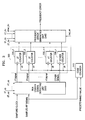
- FIG. 1 illustrates a known frequency detector installed in the PLL circuit.
- the frequency detector includes a maximum run-length detector 101, an edge counter 102, a buffer 103, first and second comparators 104_1 and 104_2, an adder 105, and a multiplexer 106.
- the maximum run-length detector 101 detects a maximum run-length mark.
- the sampled RF signal is received from an analog-to-digital converter (ADC) (not shown) installed in the PLL circuit.
- ADC analog-to-digital converter
- the sampled RF signal has a series of blocks, each having a fixed length.
- FIG. 2 is a diagram of the series of blocks.
- a head of each block is constructed using a synchronization pattern.
- the synchronization pattern includes at least one maximum run-length mark.
- the maximum run-length detector 101 of FIG. 1 detects a maximum run-length mark from the synchronization pattern.
- the edge counter 102 counts passing edges (rising edges and falling edges) of the sampled RF signal to control a frequency detection period. Thus, a predetermined value is set in the edge counter 102 such that the frequency detection period has at least a synchronization pattern.
- the edge counter 102 When the counting result reaches the predetermined value, the edge counter 102 provides a positive pulse to the maximum run-length detector 101, the buffer 103, and the multiplexer 106. Then, the maximum run-length detector 101 is cleared to start detecting a maximum run-length in a subsequent frequency detection period.
- the buffer 103 loads the maximum run-length from the maximum run-length detector 101 and the positive pulse from the edge counter 102.
- the first and second comparators 104_1 and 104_2 compare the maximum run-length loaded into the buffer 103 with a predetermined run-length.
- the first comparator 104_1 outputs "-1" when the maximum run-length loaded into the buffer 103 is greater than the predetermined run-length, and outputs "0" otherwise.
- the second comparator 104_2 outputs "+1" when the loaded maximum run-length is less than the predetermined run-length, and outputs "0” otherwise.
- the predetermined run-length is a maximum run-length.
- the maximum run-length loaded into the buffer 103 is greater than the predetermined run-length when a sampling clock frequency of the sampled RF signal is greater than a target frequency. In this case, the adder 105 outputs "-1". The maximum run-length loaded into the buffer 103 is less than the predetermined run-length when the sampling clock frequency of the sampled RF signal is less than the target frequency. In this case, the adder 105 outputs "+1". If the maximum run-length loaded into the buffer 103 is equal to the predetermined run-length, the adder 105 outputs "0". Whenever receiving a positive pulse from the edge counter 102, the multiplexer 106 outputs an output of the adder 105 as a frequency error.
- the frequency detector illustrated in FIG. 1 detects a maximum run-length mark from a synchronization pattern and generates a frequency error.
- a maximum run-length is not detected often. For instance, one or two maximum run-length marks may be detected from each block illustrated in FIG. 2. Accordingly, a frequency detection period controlled by the edge counter 102 must be set such that at least a maximum run-length mark is detected therein. Thus, there is a drawback in reducing a frequency error detection period when using the frequency detector of FIG. 1, thereby preventing a frequency error from being detected at high speed.
- a maximum run-length may be affected by noise or inter-symbol interference (ISI).
- ISI inter-symbol interference
- the performance of the frequency detector of FIG. 1 may degrade in an environment where a signal-to-noise ratio (SNR) is low and/or inter-symbol interference (ISI) is high.
- SNR signal-to-noise ratio
- ISI inter-symbol interference
- the performance of the frequency detector may not be adequate.
- SNR signal-to-noise ratio
- ISI inter-symbol interference
- a frequency detector for an optical disc reproducing system comprising: a run-length signal detecting unit which detects run-length signals from a sampled radio-frequency signal in a frequency detection period, based on a predicted distribution density of the run-length signal; a counter unit including at least one counter which counts the detected run-length signals in the frequency detection period; an edge counter which counts passing edges of the sampled radio-frequency signal to control the frequency detection period; and a frequency error generating unit which generates a frequency error in the frequency detection period, using the counting result output from the at least one counter and a predetermined reference value.
- a frequency detector for an optical disc reproducing system comprising a run-length signal detecting unit which divides a run-length region into at least two run-length regions based on a predicted distribution density of run-length signals, and detects a run-length signal from a sampled radio-frequency signal by each divided run-length region in a frequency detection period; a counter unit including a plurality of counters to count the detected run-length signals for each run-length region in the frequency detection period; an edge counter which counts passing edges of the sampled radio-frequency signal and controls the frequency detection period according to the counting result; and a frequency error generating unit which generates a frequency error in the frequency detection period, using a counter value of each of the plurality of the counters and a predetermined reference value of each run-length region.
- a frequency detector for an optical disc reproducing system comprising a run-length signal detecting unit which detects high-frequency run-length signals from a sampled radio-frequency signal, based on a predicted distribution density of run-length signals; a counter which counts run-length signals detected by the run-length signal detecting unit in a frequency detection period; an edge counter counts passing edges of the sampled radio-frequency signal and controls the frequency detection period according to the counting result; and a frequency error generating unit which generates a frequency error in the frequency detection period using a counter value output from the counter and a predetermined predicted value.
- a method of detecting a frequency error suitable for use in an optical disc reproducing system includes dividing a run-length region, in which a run-length signal is to be detected, into at least two run-length regions based on a predicted distribution density of a run-length signal; detecting run-length signals from a sampled radio-frequency signal according to each run-length region; counting the run-length signals detected in each divided run-length region; and selecting and outputting a frequency error in the frequency detection period from a plurality of predetermined frequency errors, based on a comparison of a number of run-length signals counted in each run-length region and a predetermined threshold of each divided run-length region.
- a method of detecting a frequency error in an optical disc reproducing system comprising: detecting high-frequency run-length signals from a sampled radio-frequency signal, based on a predicted distribution density of run-length signals including high-frequency and other run-length signals; counting the high-frequency run-length signals detected in a frequency detection period to produce a counting result; and generating a frequency error in the frequency detection period, using the counting result and a predicted value of the high-frequency run-length signal.
- a frequency detector in an optical disc reproducing system comprising: a run-length signal detecting unit which detects lengths of run-length signals of a sampled radio-frequency signal and separates the run-length signals into corresponding run-length regions according to the detected lengths; a plurality of counter units corresponding to the number of run-length regions to generate a counting result, each counter unit to count the detected run-length signals separated into the corresponding run-length region to provide a region counting result included in the counting result; and a frequency error generating unit which generates a frequency error using the counting result.
- a method of detecting a frequency error in an optical disc reproducing system comprising: detecting run-length signals from a sampled radio-frequency signal; assigning each of the detected run-length signals one of a plurality of run-length regions having a length corresponding to the detected run-length signals; counting the run-length signals detected in each run-length region; and outputting a frequency error based on a comparison of a number of run-length signals counted in each run-length region.
- an optical disc reproducing system including the apparatus or employing the method of any other aspect of the invention.
- FIG. 3 is a block diagram of a frequency detector according to an embodiment of the present invention.
- the frequency detector includes an edge counter 310, a run-length signal detecting unit 320, a counter unit 330, and a frequency-error generating unit 340.
- a sampled radio-frequency (RF) signal may be received from an analog-to-digital converter (ADC) (not shown) installed in a PLL circuit (not shown) with the frequency detector of FIG. 3.
- ADC analog-to-digital converter
- the RF signal can be received from a signal processing circuit, (such as a DC component remover) which is connected to an output terminal of the ADC.
- the ADC samples an input RF signal and outputs the sampled RF signal.
- the edge counter 310 Upon receiving the sampled RF signal, the edge counter 310 counts passing edges of the sampled RF signal to control a frequency detection period. The passing edges include rising edges and falling edges of the sampled RF signal. When the counting result reaches a predetermined value, the edge counter 310 outputs a signal having a positive pulse to control the frequency detection period. Also, after outputting the signal with the positive pulse, the edge counter 310 clears the counting result and counts passing edges of a subsequently sampled RF signal to control a subsequent frequency detection period. When the counting result does not reach the predetermined value, the edge counter 310 outputs "0". The signal with the positive pulse is transmitted to the counter unit 330 and the frequency-error generating unit 340.
- the predetermined value is suitably determined based on a range that allows evaluation of the distribution density of a run-length signal versus the sample RF signal.
- the run-length signal detecting unit 320 detects run-length signals from the RF signal that is sampled based on the distribution density of the run-length estimated according to channel coding characteristics of the optical disc reproducing system. Specifically, the run-length signal detecting unit 320 partitions the sampled RF signal into at least two run-length regions. The partition is based on the estimated run-length distribution density. The run-length signal detecting unit 320 then classifies and detects run-length signals of the RF signals sampled in the frequency detection period according to the corresponding run-length regions.
- the run-length signal detecting unit 320 divides the run-length region by 1T into n-1 run-length regions from a 2T run-length region to an nT run-length, and other run-length regions including run-lengths except 2T through nT run-lengths.
- the run-length signal detecting unit 320 divides the run-length region into n run-length regions, using a predetermined run-length region boundary value 2T_up, 3T_up, ..., nT_up, as illustrated in FIG. 5.
- n may be determined based on a maximum run-length of the various types of optical discs available in an optical disc reproducing system in which the frequency detector is to be used. For instance, when a compact disc (CD), a digital versatile disc (DVD), a blue-ray disc (BD), and a high-definition (HD)-DVD are available in the optical disc reproducing system, a maximum run-length of the CD is 11T, a maximum run-length of the DVD is 11T, a maximum run-length of the BD is 8T, and a maximum run-length of the HD-DVD is 11T. Therefore, n may be set to 11. Further, if compatibility is not needed with plural media, n can be set for only that media.
- the run-length signal detecting unit 320 divides the run-length region into a run-length region corresponding to a minimum run-length (e.g., 2T) and a run-length region that covers all the other run-lengths except the minimum run-length, and detects the run-length signal from the sampled RF signal.
- the run-length signal detecting unit 320 divides the run-length region into a run-length region corresponding to a run-length in which a run-length signal is most frequently detected, and a run-length region that covers the other run-lengths except the most frequently detected run-length signal, and detects a run-length signal from the sampled RF signal.
- FIGs. 4 and 5 illustrate that the minimum run-length 2T is a most frequently detected run-length, a run-length, other than the minimum run-length 2T may be the most frequently detected run-length according to other embodiments.
- the run-length signal detecting unit 320 includes a zero-crossing point detecting unit 610, a run-length signal detecting unit 620, and an enable signal generating unit 630.
- the zero-crossing point detecting unit 610 detects a zero crossing point of a sampled RF signal.
- the zero-crossing point detecting unit 610 includes a sign selector 611, a first delayer 612, an XOR gate 613, a second delayer 614, and an AND gate 615.
- the sign selector 611 transforms the sample RF signal into a rectangular shaped signal.
- the sign selector 611 outputs "1" when the sampled RF signal is positive, and outputs "0" when the sampled RF signal is negative.
- the first delayer 612 delays an output of the sign selector 611 by a sampling clock.
- the XOR gate 613 performs an exclusive or operation on outputs of the sign selector 611 and the first delayer 612, and outputs "1" when the sampled RF signal has a zero crossing point.
- the second delayer 614 delays an output of the XOR gate 613 by the sampling clock.
- the AND gate 615 performs an AND operation on the sampling clock of the optical disc reproducing system, which is output from the PLL circuit, and an output of the second delayer 614. The AND gate 615 outputs a signal with a rising edge when the sampled RF signal has a zero crossing point.
- the run-iength signal detecting unit 620 detects a run-length signal from the sampled RF signal.
- the run-length signal detecting unit 620 includes an absolute value operation unit 621, a third delayer 622, a distance operation unit 623, a multiplexer 624, a first adder 625, a fourth delayer 626, a subtracter 627, and a second adder 628.
- the absolute value operation unit 621 computes an absolute value of the sampled RF signal.
- the third delayer 622 delays an output of the absolute value operation unit 621 by the sampling clock.
- the distance operation unit 623 computes a distance d between sampled points, using the output of the absolute value operation unit 621 and an output of the third delayer 622.
- the multiplexer 624 transmits an output of the distance operation unit 623 at the zero crossing point, under control by the output of the XOR gate 613. At a point, not the zero crossing point, the multiplexer 624 transmits a signal received from the first adder 625.
- the fourth delayer 626 delays an output of the multiplexer 624 by the sampling clock.
- the first adder 625 adds 1T to the output of the multiplexer 624 and transmits the addition result to the multiplexer 624 at the point, other than the zero crossing point.
- the subtracter 627 subtracts the output of the distance operation unit 623 from 1T.
- the second adder 628 adds an output of the subtracter 627 to an output of the fourth delayer 626.
- the addition result corresponds to the run-length signal detected from the sampled RF signal.
- the multiplexer 624, the first adder 625, the fourth delayer 626, the subtracter 627, and the second adder 628 may be defined as a logic circuit 629 that detects the run-length signal by summing up 1T between zero crossing points using the outputs of the XOR gate 613 and the distance operation unit 623.
- the enable signal generating unit 630 generates an enable signal for a run-length region corresponding to the detected run-length signal, using a signal output from the zero-crossing point detecting unit 610, a signal output from the run-length signal detecting unit 620, and the predetermined run-length region boundary value 2T_up, 3T_up, ..., nT_up.
- the enable signal generating unit 630 includes a comparison array 631 and an AND gate array 632.
- other arrays can be used in other embodiments of the invention and according to other run-length region definitions.
- the comparison array 631 compares the signal output from the run-length signal detecting unit 620 with the predetermined run-length region boundary value 2T_up, 3T_up, ..., nT_up using a plurality of comparators 631_1 through 631_n.
- the comparison array 631 primarily checks the run-length region corresponding to the detected run-length signal according to the comparison result. For instance, if the run-length signal detected by the run-length signal detecting unit 620 is generated between 2T and 3T, the logic level of a signal output from the comparator 631_1 is different from those of signals output from the other comparators 631_2 through 631_n.
- the run-length signal detected by the run-length signal detecting unit 620 is generated between 3T and 4T, the logic levels of the signals output from the comparators 631_1 and 631_2 are different from those of the signals output from the other comparators 631_3 through 631_n.
- the AND gate array 632 generates an enable signal for the run-length region corresponding to the run-length signal detected by the run-length signal detecting unit 620. Specifically, the AND gate array 632 generates the enable signal by performing an AND operation on a signal output from a corresponding comparator of the comparison array 631, the signal output from the zero-crossing point detecting unit 610, and a signal output from a comparator adjacent to the corresponding comparator, using a plurality of AND gates 632_1 through 632_n.
- the run-length signal detected by the run-length signal detecting unit 620 is generated between 2T and 3T, the signal output from the comparator 631_1 is at a logic high level and the signal output from the comparator 631_2 is at a logic low level.
- the OR gate 615 of the zero-crossing point detecting unit 610 outputs a signal with a rising edge, only a 3T signal output via the AND gate 632_2 of the AND gate array 632 has a positive pulse.
- the run-length signal detected by the run-length signal detecting unit 620 is generated between 3T and 4T, the signals output from the comparators 631_1 and 631_2 are at a logic high level and the signal output from the comparator 631_3 is at a logic low level.
- the OR gate 615 of the zero-crossing point detecting unit 610 outputs a signal with a rising edge, only a 4T signal output via the AND gate 632_3 of the AND gate array 632 has a positive pulse.
- the AND gate 632_1 corresponding to a 2T signal does not consider the output of the comparator adjacent to the corresponding comparator.
- a run-length region boundary value set in the comparator adjacent to the corresponding comparator is smaller than that set in the corresponding comparator.
- the corresponding comparator is the comparator 631_2 and the adjacent comparator is the comparator 631_1.
- Enable signals output from the enable signal generating unit 630 are transmitted to the counter unit 330.
- the counter unit 330 includes at least a counter that counts the run-length signal detected by the run-length signal detecting unit 320 during a frequency detection period. Referring to FIG. 3, the counter unit 330 includes n counters 330_1 through 330_n, since the run-length signal detecting unit 320 uses n run-length regions. Accordingly, a total number of counters to be installed in the counter unit 330 is determined by a total number of run-length regions available in the run-length signal detecting unit 320.
- run-length regions available in the run-length signal detecting unit 320 include n-1 run-length regions, from a 2T run-length region to an nT run-length region, which are divided into 1T units, except the 2T to nT run-lengths. Therefore, the n counters 330_1 through 330_n include a 2T counter 330_1 corresponding to a 2T run-length, a 3T counter 330_2 corresponding to a 3T run-length, ..., an nT counter 330_n-1 corresponding to an nT run-length, and the other counter 330_n corresponding to a run-length except the 2T to nT run-lengths.
- the 2T counter 330_1 counts up whenever the run-length signal detecting unit 320 outputs a 2T signal having a positive pulse.
- the 3T counter 330_2 counts up whenever the run-length signal detecting unit 320 outputs a 3T signal having a positive pulse.
- the nT counter 330_n-1 counts up whenever the run-length signal detecting unit 320 outputs an nT signal having a positive pulse.
- the other counter 330_n counts up whenever the run-length signal detecting unit 320 outputs the other signal having a positive pulse.
- count values of the 2T through the other counters 330_1 through 330_n are cleared.
- the count value of the 2T counter 330_1 indicates the number of 2T run-length signals generated during the frequency detection period.
- the count value of the 3T counter 330_2 indicates the number of 3T run-length signals generated during the frequency detection period.
- the count value of the nT counter 330_n-1 indicates the number of nT run-length signals generated during the frequency detection period.
- the count value of the other counter 330_n indicates the number of other run-length signals generated during the frequency detection period.
- the counter unit 330 may include two counters, each corresponding to each of the two run-length regions, and operate as described above.
- the frequency-error generating unit 340 generates a frequency error in the frequency detection period, using the count values of the n counters 330_1 through 330_n of the counter unit 330 and predetermined reference values 2T_thr through other_thr.
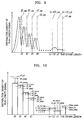
- Each of the predetermined reference values 2T_thr through other thr is a threshold that is determined based on an estimated distribution density of a run-length signal that can be generated in a corresponding run-length region in the frequency detection period. That is, when the frequency of a sampling clock of an optical disc reproducing system, which is output from the PLL circuit, is lower than a target frequency, a graph shown in FIG.
- FIG. 8 is a graph illustrating the relationship between an actual number nT_count of run-length signals generated in each run-length region, a predicted number nT_ideal of the run-length signals, and a threshold nT_thr determined based on the predetermined number nT_ideal, when the distribution density of the run-length signal changes as illustrated in FIG. 7.
- FIG. 10 is a graph illustrating the relationship between an actual number nT_count of run-length signals generated in each run-length region, a predicted number nT_ideal of the run-length signals, and a threshold nT_thr determined based on the predetermined number nT_ideal, when the distribution density of the run-length signal in each run-length region changes as illustrated in FIG. 9. As illustrated in FIG. 10
- the actual number nT_count may be less than the predicted number nT_ideal in a run-length region corresponding to a short run-length, e.g., 2T, and the actual number nT_count may be greater than the threshold nT_thr that is determined based on the predicted number nT_ideal in a run-length region corresponding to a run-length greater than 2T.
- the predetermined reference value may be determined, based on the threshold that is described with reference to FIGs. 7 through 10 and the actual number of run-length signals generated.
- FIG. 11 is a detailed diagram of the frequency-error generating unit 340 according to an embodiment of the present invention.
- the frequency-error generating unit 340 includes a comparison array 1110, a logic table 1120, and a multiplexer 1130.
- the comparison array 1110 includes a plurality of comparators 1110_1 through 1110_n that correspond to the plurality of the counters 330_1 through 330_n of the counter unit 330, respectively.
- the comparators 1110_1 through 1110_n compare a counter value of each of the counters 330_1 through 330_n with the predetermined reference value 2T_thr, ..., other throf a corresponding run-length region.
- the comparators 1110_1 through 1110_n output signals input [n-1] through input [0], which are indicative of the comparison results, to the logic table 1120.
- the logic table 1120 selects and outputs one of a plurality of predetermined frequency errors, in response to the signals input [n-1] through input [0]. As illustrated in FIG. 11, the logic table 1120 has a structure by connecting each combination of bits that can be generated according to the comparison results output from the comparison array 1110 and a frequency error corresponding to each combination of bits. A frequency error output from the logic table 1120 is transmitted to the multiplexer 1130. It is understood that the logic table 1120 can store these combinations in a memory of the logic table 1120 or can recall the logic table 1120 e.g. from another memory included in a recording and/or reproducing apparatus.
- the multiplexer 1130 transmits a signal output from the logic table 1120 as a frequency error. As described above with respect to the edge counter 310, the output enable signal out_en is applied as a positive-pulse signal. When the output enable signal out_en is not provided, the multiplexer 1130 transmits "0".
- FIG. 12 is a block diagram of a frequency detector according to another embodiment of the present invention.
- the frequency detector includes a run-length signal detecting unit 1201, an edge counter 1202, a counter 1203, and a frequency error generating unit 1204.
- the run-length signal detecting unit 1201 detects a high-frequency run-length signal from a sampled RF signal, based on the predicted distribution density of the run-length signal according to the channel coding characteristics of an optical disc reproducing system, which is described with reference to FIG. 3.
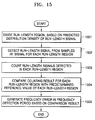
- the run-length signal detecting unit 1201 is constructed as illustrated in FIG. 13.
- FIG. 13 is a detailed block diagram of the run-length signal detecting unit 1201 according to an embodiment of the present invention.
- the run-length signal detecting unit 1201 includes a zero crossing point detecting unit 1310, a run-length signal detecting unit 1320, and an enable signal generating unit 1330.
- the zero crossing point detecting unit 1310 detects a zero crossing point of the sampled RF signal.
- the zero crossing point detecting unit 1310 includes a sign selector 1311, a first delayer 1312, an XOR gate 1313, a second delayer 1314, and an AND gate 1315.
- the construction of the zero crossing point detecting unit 1310 is similar to that of the zero-crossing point detecting unit 610 of FIG. 6 in the shown embodiment.
- the run-length signal detecting unit 1320 detects the run-length signal from the sampled RF signal.
- the run-length signal detecting unit 1320 includes an absolute value operation unit 1321, a delayer 1322, a distance operation unit 1323, and a logic circuit 1329.
- the construction of the run-length signal detecting unit 1320 is similar to that of the run-length signal detecting unit 620 of FIG. 6 in the shown embodiment.
- the enable signal generating unit 1330 generates an enable signal based on whether the high-frequency run-length signal is detected, using the result of comparing a least upper bound xT_up and a greatest lower bound xT_low determined based on the high frequency run-length signal with the run-length signal detected by the run-length signal detecting unit 1320, and the signal output from the zero crossing point detecting unit 1310. Therefore, as illustrated in FIG.
- the enable signal generating unit 1330 includes a first comparator 1331 that compares the least upper bound xT_up with an output of the run-length signal detecting unit 1320; a second comparator 1332 that compares the greatest lower bound xT_low with the output of the run-length signal detecting unit 1320; and an AND gate 1333 that performs an AND operation on outputs of the zero crossing point detecting unit 1310 and the first and second comparators 1331 and 1332 and outputs an enable signal xTsignal as the operation result.
- the least upper bound xT_up and the greatest lower bound xT_low may be set to 2.5T and 0, respectively. If the run-length in which the run-length signal is generated most frequently is greater than 2T, the least upper bound xT_up may be set to a very large value or an infinite value, and the greatest lower bound xT_low may be set to 2.5T.
- the operation of the edge counter 1202 is the same as that of the edge counter 310 of FIG. 3 in the shown embodiment.
- the counter 1203 counts run-length signals detected by the run-length signal detecting unit 1201 in the frequency detection period, and transmits the counting result to the frequency error generating unit 1204.
- the counting result of the counter 1203 is cleared by the edge counter 1202.
- the frequency error generating unit 1204 generates a frequency error in the frequency detection period, using the counting result output from the counter 1203 and a predetermined predicted value.
- FIG. 14 is a detailed circuit diagram of the frequency error generating unit 1204 for use in an embodiment of the present invention.
- the frequency error generating unit 1204 includes a subtracter 1401, an amplifier 1402, and a multiplexer 1403.
- the subtracter 1401 subtracts a counter value xT_count, which is output from the counter 1203, from a predetermined predicted value xT_ideal.
- the counter value xT_count indicates a number of high-frequency run-length signals generated in the frequency detection period.
- the predetermined predicted value indicates a predicted number xT_ideal (or a predicted distribution density) of run-length signals generated in a run-length region corresponding to a run-length in which a run-length signal is generated most frequently.
- the predetermined predicted value may be defined as a predetermined reference value that is different from the predetermined reference value described with respect to FIG. 3.
- the amplifier 1402 amplifies the subtracting result output from the subtracter 1401 to a predetermined value according to a predetermined gain.
- the multiplexer 1403 transmits an output of the amplifier 1402 as a frequency error.
- the output enable signal out_en may be a positive pulse signal.
- the multiplexer 1403 outputs "0" when the output enable signal out_en is not provided.
- FIG. 15 is a flowchart illustrating a method of detecting a frequency error according to another embodiment of the present invention.
- a run-length region in which a run-length signal can be detected is divided into at least two run-length regions, based on the distribution density of the run-length signal which is predicted according to the channel coding characteristics of an optical disc reproducing system (1501).
- a run-length signal is detected from a sampled RF signal by each run-length region (1502). Run-length signals detected are counted in each run-length region, as described above with reference to the counter unit 330 of FIG. 3 (1503).
- a frequency error in a frequency detection period is selected and output from a plurality of predetermined frequency errors, based on a comparison of the counting result for each run-length region and a predetermined reference value for each run-length (1504 and 1505).
- the predetermined reference value is equal to the predetermined reference value used by the frequency-error generating unit 340 of FIG. 3.
- FIG. 16 is a flowchart illustrating a method of detecting a frequency error according to another embodiment of the present invention.
- a run-length signal of high frequency is detected from a sampled RF signal, based on the distribution density of a run-length signal predicted according to the channel coding characteristics of an optical disc reproducing system (1601).
- a number of run-length signals of high frequency detected in the frequency detection period is counted, as described above with reference to the counter 1203 of FIG. 12 (1602).
- a frequency error in the frequency detection period is generated, using the counting result and a predicted value of the run-length signal of high frequency (1603).
- the frequency error is generated by subtracting the counting result from the predicted value, as described above with respect to the frequency error generating unit 1204 of FIG. 12.
- the values used by the logic table 1120, the thresholds 2T_thr, ..., other_thr, and other predetermined numbers can be adjusted and/or updated according to usage of the apparatus and/or through software updates in order to increase the accuracy of the frequency error detection and/or the predicted distribution density.
- a program that executes a method of detecting a frequency error according to the present invention can be embodied as computer readable code in at least one computer readable medium.
- the computer readable medium may be any recording apparatus capable of storing data that is read by a computer system, e.g., read-only memory (ROM), random access memory (RAM), a compact disc (CD)-ROM, a magnetic tape, a floppy disk, an optical data storage device, and so on.
- the computer readable medium may be a carrier wave that transmits data via the Internet, for example.
- the computer readable medium can be distributed among computer systems that are interconnected through a network, and the present invention may be stored and implemented as a computer readable code in the distributed system.
- a frequency error is generated by collecting run-length information from an RF signal sampled based on the distribution density of a run-length signal, which is predicted according to the channel coding characteristics of an optical disc reproducing system. Accordingly, it is possible to more rapidly detect a frequency error than when using a conventional method.
- a frequency error is generated by collecting information regarding a run-length in which a run-length signal is detected more frequently, as run-length information regarding the sampled RF signal, based on the predicted distribution density of the run-length signal, thereby realizing a frequency detector that is less sensitive to noise and inter-symbol interference (ISI). Accordingly, it is possible to improve the frequency error detecting performance of a PLL circuit in a system, such as a high-density optical disc reproducing system, which has low noise characteristics and high ISI characteristics.
- ISI inter-symbol interference
- FIG. 17 is a block diagram of a recording and/or reproducing apparatus according to an embodiment of the present invention.
- the recording apparatus includes a recording/reading unit 1701, a controller 1702, and a memory 1703.
- the recording/reading unit 1701 records data on a disc 1700, and reads the data from the disc 1700.
- the controller 1702 records and reproduces disc related data using the PLL circuit according to the present invention as set forth above in relation to FIGs. 3 through 16.
- the controller 1702 can be computer implementing the method using a computer program encoded on a computer readable medium.
- the computer can be implemented as a chip having firmware, or can be a general or special purpose computer programmable to perform the method.
- the recording/reading unit 1701 could include a low wavelength, high numerical aperture type unit usable to record dozens of gigabytes of data on the disc 1700.
- Examples of such units include, but are not limited to, those units using light wavelengths of 405 nm and having numerical apertures of 0.85, those units compatible with Blu-ray discs, and/or those units compatible with Advanced Optical Discs (AOD).
Landscapes
- Engineering & Computer Science (AREA)
- Signal Processing (AREA)
- Signal Processing For Digital Recording And Reproducing (AREA)
- Stabilization Of Oscillater, Synchronisation, Frequency Synthesizers (AREA)
- Optical Recording Or Reproduction (AREA)
- Moving Of The Head For Recording And Reproducing By Optical Means (AREA)
- Manipulation Of Pulses (AREA)
- Measuring Frequencies, Analyzing Spectra (AREA)
Applications Claiming Priority (1)
| Application Number | Priority Date | Filing Date | Title |
|---|---|---|---|
| KR1020050049696A KR100694125B1 (ko) | 2005-06-10 | 2005-06-10 | 위상 동기 루프 회로에서의 주파수 검출기 및 주파수 에러검출 방법 |
Publications (2)
| Publication Number | Publication Date |
|---|---|
| EP1734530A1 true EP1734530A1 (de) | 2006-12-20 |
| EP1734530B1 EP1734530B1 (de) | 2007-12-12 |
Family
ID=37000083
Family Applications (1)
| Application Number | Title | Priority Date | Filing Date |
|---|---|---|---|
| EP06252883A Not-in-force EP1734530B1 (de) | 2005-06-10 | 2006-06-03 | Auf Run-length basierender Frequenzdetektor für eine Phasenregelschleife und dazu gehöriges Verfahren |
Country Status (8)
| Country | Link |
|---|---|
| US (1) | US20060279440A1 (de) |
| EP (1) | EP1734530B1 (de) |
| JP (1) | JP2006352867A (de) |
| KR (1) | KR100694125B1 (de) |
| CN (1) | CN1877731A (de) |
| AT (1) | ATE381098T1 (de) |
| DE (1) | DE602006000313T2 (de) |
| TW (1) | TW200644437A (de) |
Families Citing this family (10)
| Publication number | Priority date | Publication date | Assignee | Title |
|---|---|---|---|---|
| US7743086B2 (en) * | 2007-06-14 | 2010-06-22 | Microsoft Corporation | Distributed kernel density estimation |
| US8019028B1 (en) * | 2008-03-26 | 2011-09-13 | Pmc-Sierra, Inc. | Run-length based spectral analysis |
| CN101335032B (zh) * | 2008-08-06 | 2011-06-15 | 凌阳科技股份有限公司 | 判断光盘片种类的方法与装置 |
| CN101656536B (zh) * | 2008-08-18 | 2012-06-20 | 中芯国际集成电路制造(上海)有限公司 | 锁相环及其锁定检测装置和方法 |
| US7932761B1 (en) * | 2009-02-09 | 2011-04-26 | Altera Corporation | Fine tuned pulse width modulation |
| CN102299710B (zh) * | 2010-06-23 | 2013-06-19 | 奇岩电子股份有限公司 | 具有改进相位检测机制的锁相环 |
| CN102468830B (zh) * | 2010-11-16 | 2016-01-20 | 北京中电华大电子设计有限责任公司 | 一种利用多相位信号提高频率比较器精度的方法和电路 |
| US9025712B2 (en) * | 2013-07-30 | 2015-05-05 | Pixart Imaging Inc. | Sensor, clock frequency adjusting system and method thereof |
| TWI820783B (zh) * | 2022-07-04 | 2023-11-01 | 華邦電子股份有限公司 | 時脈信號的頻率偵測裝置及其偵測方法 |
| CN116489617B (zh) * | 2023-04-11 | 2026-03-27 | 重庆希微科技有限公司 | 窄带信号检测、频率估计和干扰消除方法、程序和设备 |
Citations (4)
| Publication number | Priority date | Publication date | Assignee | Title |
|---|---|---|---|---|
| EP0997902A2 (de) * | 1998-10-28 | 2000-05-03 | Victor Company of Japan, Ltd. | Frequenzsteuergerät und Wiedergabegerät von digitalen Signalen |
| US20020071194A1 (en) * | 2000-12-07 | 2002-06-13 | Nec Corporation | PLL circuit, data detection circuit and disk apparatus |
| US20030043939A1 (en) * | 2001-05-28 | 2003-03-06 | Tetsuya Okumura | Signal evaluation devices and signal evaluation methods, signal quality evaluation methods and reproducing devices and recording devices |
| WO2004038719A2 (en) * | 2002-10-23 | 2004-05-06 | Matsushita Electric Industrial Co., Ltd. | Frequency and phase control apparatus and maximum likelihood decoder |
Family Cites Families (10)
| Publication number | Priority date | Publication date | Assignee | Title |
|---|---|---|---|---|
| US5424881A (en) * | 1993-02-01 | 1995-06-13 | Cirrus Logic, Inc. | Synchronous read channel |
| GB2274956B (en) * | 1993-02-05 | 1997-04-02 | Sony Broadcast & Communication | Image data compression |
| JPH11149704A (ja) * | 1997-11-19 | 1999-06-02 | Sony Corp | フェーズロックドループ回路、再生装置、及びフェーズロックドループ回路の引き込み制御方法 |
| JPH11149703A (ja) * | 1997-11-19 | 1999-06-02 | Sony Corp | 回転速度制御装置、再生装置及び回転速度制御方法 |
| KR100318842B1 (ko) * | 1998-11-26 | 2002-04-22 | 윤종용 | 디지털위상제어루프에서의주파수검출방법 |
| TW518845B (en) * | 2001-03-30 | 2003-01-21 | Ali Corp | Method of erroneous data correction for full response channel system |
| JP3838972B2 (ja) * | 2002-12-25 | 2006-10-25 | Necエレクトロニクス株式会社 | 周波数検出回路及びデータ処理装置 |
| JP3972868B2 (ja) * | 2003-06-24 | 2007-09-05 | ソニー株式会社 | デジタルpll装置 |
| JP3960271B2 (ja) * | 2003-07-02 | 2007-08-15 | ソニー株式会社 | 位相誤差判定方法、デジタルpll装置 |
| US7436752B2 (en) * | 2005-11-17 | 2008-10-14 | Realtek Semiconductor Corp. | Method and apparatus for signal equalization in a light storage system |
-
2005
- 2005-06-10 KR KR1020050049696A patent/KR100694125B1/ko not_active Expired - Fee Related
-
2006
- 2006-04-19 US US11/406,374 patent/US20060279440A1/en not_active Abandoned
- 2006-06-03 AT AT06252883T patent/ATE381098T1/de not_active IP Right Cessation
- 2006-06-03 DE DE602006000313T patent/DE602006000313T2/de not_active Expired - Fee Related
- 2006-06-03 EP EP06252883A patent/EP1734530B1/de not_active Not-in-force
- 2006-06-05 TW TW095119809A patent/TW200644437A/zh unknown
- 2006-06-09 JP JP2006161212A patent/JP2006352867A/ja active Pending
- 2006-06-12 CN CNA2006100918324A patent/CN1877731A/zh active Pending
Patent Citations (4)
| Publication number | Priority date | Publication date | Assignee | Title |
|---|---|---|---|---|
| EP0997902A2 (de) * | 1998-10-28 | 2000-05-03 | Victor Company of Japan, Ltd. | Frequenzsteuergerät und Wiedergabegerät von digitalen Signalen |
| US20020071194A1 (en) * | 2000-12-07 | 2002-06-13 | Nec Corporation | PLL circuit, data detection circuit and disk apparatus |
| US20030043939A1 (en) * | 2001-05-28 | 2003-03-06 | Tetsuya Okumura | Signal evaluation devices and signal evaluation methods, signal quality evaluation methods and reproducing devices and recording devices |
| WO2004038719A2 (en) * | 2002-10-23 | 2004-05-06 | Matsushita Electric Industrial Co., Ltd. | Frequency and phase control apparatus and maximum likelihood decoder |
Also Published As
| Publication number | Publication date |
|---|---|
| DE602006000313T2 (de) | 2008-12-11 |
| CN1877731A (zh) | 2006-12-13 |
| EP1734530B1 (de) | 2007-12-12 |
| TW200644437A (en) | 2006-12-16 |
| KR20060128336A (ko) | 2006-12-14 |
| US20060279440A1 (en) | 2006-12-14 |
| ATE381098T1 (de) | 2007-12-15 |
| JP2006352867A (ja) | 2006-12-28 |
| KR100694125B1 (ko) | 2007-03-12 |
| DE602006000313D1 (de) | 2008-01-24 |
Similar Documents
| Publication | Publication Date | Title |
|---|---|---|
| KR100629509B1 (ko) | 광디스크에서 독출된 신호의 신호대 잡음비 측정 장치 및그 방법 | |
| JP3821472B2 (ja) | 異常波形検出回路および情報再生装置 | |
| EP1734530B1 (de) | Auf Run-length basierender Frequenzdetektor für eine Phasenregelschleife und dazu gehöriges Verfahren | |
| US8385173B2 (en) | Method for determining characteristics of signal and apparatus using the same | |
| US7321531B2 (en) | Apparatus for reproducing data from optical storage medium using multiple detector | |
| KR100750126B1 (ko) | 위상 동기 루프 회로 및 위상 동기 루프 제어 방법 | |
| CN1271166A (zh) | 空白检测电路和方法 | |
| KR100708110B1 (ko) | 워블 신호를 이용한 시스템 클록 생성 장치 및 그를이용한 데이터 재생 장치 | |
| JP2009527069A (ja) | 信号品質評価装置及び方法並びに光ディスクドライバ | |
| JP5153827B2 (ja) | 信号特性決定装置、信号特性決定方法、及び記録媒体 | |
| US7613093B2 (en) | Duty ratio control apparatus for pre-pit detection or header detection of an optical storage medium | |
| US7599271B2 (en) | Optical disk apparatus | |
| KR20010090263A (ko) | 광 기록재생기의 알에프 신호 제어 방법 및 장치 | |
| KR20010036087A (ko) | 고밀도 디스크 기록매체와 그에 따른 데이터 재생장치 및 방법 | |
| US20040105366A1 (en) | Information storage medium, and data recording, reproducing, detecting and/or evaluating apparatus and method using the same | |
| JP2004030924A (ja) | デジタルフェーズロックドループ回路 | |
| JP2009032348A (ja) | 光ディスク再生装置 | |
| JP2007012101A (ja) | 光ディスク再生装置 |
Legal Events
| Date | Code | Title | Description |
|---|---|---|---|
| PUAI | Public reference made under article 153(3) epc to a published international application that has entered the european phase |
Free format text: ORIGINAL CODE: 0009012 |
|
| 17P | Request for examination filed |
Effective date: 20060621 |
|
| AK | Designated contracting states |
Kind code of ref document: A1 Designated state(s): AT BE BG CH CY CZ DE DK EE ES FI FR GB GR HU IE IS IT LI LT LU LV MC NL PL PT RO SE SI SK TR |
|
| AX | Request for extension of the european patent |
Extension state: AL BA HR MK YU |
|
| 17Q | First examination report despatched |
Effective date: 20070219 |
|
| GRAP | Despatch of communication of intention to grant a patent |
Free format text: ORIGINAL CODE: EPIDOSNIGR1 |
|
| AKX | Designation fees paid |
Designated state(s): AT BE BG CH CY CZ DE DK EE ES FI FR GB GR HU IE IS IT LI LT LU LV MC NL PL PT RO SE SI SK TR |
|
| GRAS | Grant fee paid |
Free format text: ORIGINAL CODE: EPIDOSNIGR3 |
|
| GRAA | (expected) grant |
Free format text: ORIGINAL CODE: 0009210 |
|
| AK | Designated contracting states |
Kind code of ref document: B1 Designated state(s): AT BE BG CH CY CZ DE DK EE ES FI FR GB GR HU IE IS IT LI LT LU LV MC NL PL PT RO SE SI SK TR |
|
| REG | Reference to a national code |
Ref country code: GB Ref legal event code: FG4D |
|
| REG | Reference to a national code |
Ref country code: CH Ref legal event code: EP |
|
| REG | Reference to a national code |
Ref country code: IE Ref legal event code: FG4D |
|
| REF | Corresponds to: |
Ref document number: 602006000313 Country of ref document: DE Date of ref document: 20080124 Kind code of ref document: P |
|
| PG25 | Lapsed in a contracting state [announced via postgrant information from national office to epo] |
Ref country code: SE Free format text: LAPSE BECAUSE OF FAILURE TO SUBMIT A TRANSLATION OF THE DESCRIPTION OR TO PAY THE FEE WITHIN THE PRESCRIBED TIME-LIMIT Effective date: 20080312 Ref country code: CH Free format text: LAPSE BECAUSE OF FAILURE TO SUBMIT A TRANSLATION OF THE DESCRIPTION OR TO PAY THE FEE WITHIN THE PRESCRIBED TIME-LIMIT Effective date: 20071212 Ref country code: LI Free format text: LAPSE BECAUSE OF FAILURE TO SUBMIT A TRANSLATION OF THE DESCRIPTION OR TO PAY THE FEE WITHIN THE PRESCRIBED TIME-LIMIT Effective date: 20071212 |
|
| PG25 | Lapsed in a contracting state [announced via postgrant information from national office to epo] |
Ref country code: NL Free format text: LAPSE BECAUSE OF FAILURE TO SUBMIT A TRANSLATION OF THE DESCRIPTION OR TO PAY THE FEE WITHIN THE PRESCRIBED TIME-LIMIT Effective date: 20071212 Ref country code: SI Free format text: LAPSE BECAUSE OF FAILURE TO SUBMIT A TRANSLATION OF THE DESCRIPTION OR TO PAY THE FEE WITHIN THE PRESCRIBED TIME-LIMIT Effective date: 20071212 Ref country code: LV Free format text: LAPSE BECAUSE OF FAILURE TO SUBMIT A TRANSLATION OF THE DESCRIPTION OR TO PAY THE FEE WITHIN THE PRESCRIBED TIME-LIMIT Effective date: 20071212 Ref country code: FI Free format text: LAPSE BECAUSE OF FAILURE TO SUBMIT A TRANSLATION OF THE DESCRIPTION OR TO PAY THE FEE WITHIN THE PRESCRIBED TIME-LIMIT Effective date: 20071212 Ref country code: LT Free format text: LAPSE BECAUSE OF FAILURE TO SUBMIT A TRANSLATION OF THE DESCRIPTION OR TO PAY THE FEE WITHIN THE PRESCRIBED TIME-LIMIT Effective date: 20071212 Ref country code: PL Free format text: LAPSE BECAUSE OF FAILURE TO SUBMIT A TRANSLATION OF THE DESCRIPTION OR TO PAY THE FEE WITHIN THE PRESCRIBED TIME-LIMIT Effective date: 20071212 |
|
| NLV1 | Nl: lapsed or annulled due to failure to fulfill the requirements of art. 29p and 29m of the patents act | ||
| REG | Reference to a national code |
Ref country code: CH Ref legal event code: PL |
|
| PG25 | Lapsed in a contracting state [announced via postgrant information from national office to epo] |
Ref country code: AT Free format text: LAPSE BECAUSE OF FAILURE TO SUBMIT A TRANSLATION OF THE DESCRIPTION OR TO PAY THE FEE WITHIN THE PRESCRIBED TIME-LIMIT Effective date: 20071212 |
|
| PG25 | Lapsed in a contracting state [announced via postgrant information from national office to epo] |
Ref country code: IS Free format text: LAPSE BECAUSE OF FAILURE TO SUBMIT A TRANSLATION OF THE DESCRIPTION OR TO PAY THE FEE WITHIN THE PRESCRIBED TIME-LIMIT Effective date: 20080412 Ref country code: ES Free format text: LAPSE BECAUSE OF FAILURE TO SUBMIT A TRANSLATION OF THE DESCRIPTION OR TO PAY THE FEE WITHIN THE PRESCRIBED TIME-LIMIT Effective date: 20080323 Ref country code: CZ Free format text: LAPSE BECAUSE OF FAILURE TO SUBMIT A TRANSLATION OF THE DESCRIPTION OR TO PAY THE FEE WITHIN THE PRESCRIBED TIME-LIMIT Effective date: 20071212 |
|
| ET | Fr: translation filed | ||
| PG25 | Lapsed in a contracting state [announced via postgrant information from national office to epo] |
Ref country code: SK Free format text: LAPSE BECAUSE OF FAILURE TO SUBMIT A TRANSLATION OF THE DESCRIPTION OR TO PAY THE FEE WITHIN THE PRESCRIBED TIME-LIMIT Effective date: 20071212 Ref country code: RO Free format text: LAPSE BECAUSE OF FAILURE TO SUBMIT A TRANSLATION OF THE DESCRIPTION OR TO PAY THE FEE WITHIN THE PRESCRIBED TIME-LIMIT Effective date: 20071212 Ref country code: BE Free format text: LAPSE BECAUSE OF FAILURE TO SUBMIT A TRANSLATION OF THE DESCRIPTION OR TO PAY THE FEE WITHIN THE PRESCRIBED TIME-LIMIT Effective date: 20071212 |
|
| PG25 | Lapsed in a contracting state [announced via postgrant information from national office to epo] |
Ref country code: PT Free format text: LAPSE BECAUSE OF FAILURE TO SUBMIT A TRANSLATION OF THE DESCRIPTION OR TO PAY THE FEE WITHIN THE PRESCRIBED TIME-LIMIT Effective date: 20080512 |
|
| PLBE | No opposition filed within time limit |
Free format text: ORIGINAL CODE: 0009261 |
|
| STAA | Information on the status of an ep patent application or granted ep patent |
Free format text: STATUS: NO OPPOSITION FILED WITHIN TIME LIMIT |
|
| PG25 | Lapsed in a contracting state [announced via postgrant information from national office to epo] |
Ref country code: DK Free format text: LAPSE BECAUSE OF FAILURE TO SUBMIT A TRANSLATION OF THE DESCRIPTION OR TO PAY THE FEE WITHIN THE PRESCRIBED TIME-LIMIT Effective date: 20071212 |
|
| PGFP | Annual fee paid to national office [announced via postgrant information from national office to epo] |
Ref country code: DE Payment date: 20080730 Year of fee payment: 3 |
|
| 26N | No opposition filed |
Effective date: 20080915 |
|
| PG25 | Lapsed in a contracting state [announced via postgrant information from national office to epo] |
Ref country code: GR Free format text: LAPSE BECAUSE OF FAILURE TO SUBMIT A TRANSLATION OF THE DESCRIPTION OR TO PAY THE FEE WITHIN THE PRESCRIBED TIME-LIMIT Effective date: 20080313 Ref country code: MC Free format text: LAPSE BECAUSE OF NON-PAYMENT OF DUE FEES Effective date: 20080630 |
|
| PG25 | Lapsed in a contracting state [announced via postgrant information from national office to epo] |
Ref country code: IE Free format text: LAPSE BECAUSE OF NON-PAYMENT OF DUE FEES Effective date: 20080603 Ref country code: EE Free format text: LAPSE BECAUSE OF FAILURE TO SUBMIT A TRANSLATION OF THE DESCRIPTION OR TO PAY THE FEE WITHIN THE PRESCRIBED TIME-LIMIT Effective date: 20071212 Ref country code: BG Free format text: LAPSE BECAUSE OF FAILURE TO SUBMIT A TRANSLATION OF THE DESCRIPTION OR TO PAY THE FEE WITHIN THE PRESCRIBED TIME-LIMIT Effective date: 20080312 |
|
| PG25 | Lapsed in a contracting state [announced via postgrant information from national office to epo] |
Ref country code: CY Free format text: LAPSE BECAUSE OF FAILURE TO SUBMIT A TRANSLATION OF THE DESCRIPTION OR TO PAY THE FEE WITHIN THE PRESCRIBED TIME-LIMIT Effective date: 20071212 |
|
| REG | Reference to a national code |
Ref country code: FR Ref legal event code: ST Effective date: 20100226 |
|
| PG25 | Lapsed in a contracting state [announced via postgrant information from national office to epo] |
Ref country code: FR Free format text: LAPSE BECAUSE OF NON-PAYMENT OF DUE FEES Effective date: 20090630 |
|
| PGFP | Annual fee paid to national office [announced via postgrant information from national office to epo] |
Ref country code: FR Payment date: 20080516 Year of fee payment: 3 |
|
| PG25 | Lapsed in a contracting state [announced via postgrant information from national office to epo] |
Ref country code: DE Free format text: LAPSE BECAUSE OF NON-PAYMENT OF DUE FEES Effective date: 20100101 |
|
| PG25 | Lapsed in a contracting state [announced via postgrant information from national office to epo] |
Ref country code: HU Free format text: LAPSE BECAUSE OF FAILURE TO SUBMIT A TRANSLATION OF THE DESCRIPTION OR TO PAY THE FEE WITHIN THE PRESCRIBED TIME-LIMIT Effective date: 20080613 Ref country code: LU Free format text: LAPSE BECAUSE OF NON-PAYMENT OF DUE FEES Effective date: 20080603 |
|
| PG25 | Lapsed in a contracting state [announced via postgrant information from national office to epo] |
Ref country code: TR Free format text: LAPSE BECAUSE OF FAILURE TO SUBMIT A TRANSLATION OF THE DESCRIPTION OR TO PAY THE FEE WITHIN THE PRESCRIBED TIME-LIMIT Effective date: 20071212 |
|
| GBPC | Gb: european patent ceased through non-payment of renewal fee |
Effective date: 20100603 |
|
| PG25 | Lapsed in a contracting state [announced via postgrant information from national office to epo] |
Ref country code: IT Free format text: LAPSE BECAUSE OF FAILURE TO SUBMIT A TRANSLATION OF THE DESCRIPTION OR TO PAY THE FEE WITHIN THE PRESCRIBED TIME-LIMIT Effective date: 20071212 |
|
| PG25 | Lapsed in a contracting state [announced via postgrant information from national office to epo] |
Ref country code: GB Free format text: LAPSE BECAUSE OF NON-PAYMENT OF DUE FEES Effective date: 20100603 |