EP1734594A2 - Dispostif électronique moléculaire - Google Patents
Dispostif électronique moléculaire Download PDFInfo
- Publication number
- EP1734594A2 EP1734594A2 EP06011764A EP06011764A EP1734594A2 EP 1734594 A2 EP1734594 A2 EP 1734594A2 EP 06011764 A EP06011764 A EP 06011764A EP 06011764 A EP06011764 A EP 06011764A EP 1734594 A2 EP1734594 A2 EP 1734594A2
- Authority
- EP
- European Patent Office
- Prior art keywords
- electron conjugated
- skeleton
- molecule
- functional molecular
- adsorbing
- Prior art date
- Legal status (The legal status is an assumption and is not a legal conclusion. Google has not performed a legal analysis and makes no representation as to the accuracy of the status listed.)
- Withdrawn
Links
Images






Classifications
-
- H—ELECTRICITY
- H10—SEMICONDUCTOR DEVICES; ELECTRIC SOLID-STATE DEVICES NOT OTHERWISE PROVIDED FOR
- H10P—GENERIC PROCESSES OR APPARATUS FOR THE MANUFACTURE OR TREATMENT OF DEVICES COVERED BY CLASS H10
- H10P10/00—Bonding of wafers, substrates or parts of devices
-
- B—PERFORMING OPERATIONS; TRANSPORTING
- B82—NANOTECHNOLOGY
- B82Y—SPECIFIC USES OR APPLICATIONS OF NANOSTRUCTURES; MEASUREMENT OR ANALYSIS OF NANOSTRUCTURES; MANUFACTURE OR TREATMENT OF NANOSTRUCTURES
- B82Y10/00—Nanotechnology for information processing, storage or transmission, e.g. quantum computing or single electron logic
-
- G—PHYSICS
- G11—INFORMATION STORAGE
- G11C—STATIC STORES
- G11C13/00—Digital stores characterised by the use of storage elements not covered by groups G11C11/00, G11C23/00, or G11C25/00
- G11C13/0002—Digital stores characterised by the use of storage elements not covered by groups G11C11/00, G11C23/00, or G11C25/00 using resistive RAM [RRAM] elements
- G11C13/0009—RRAM elements whose operation depends upon chemical change
- G11C13/0014—RRAM elements whose operation depends upon chemical change comprising cells based on organic memory material
-
- G—PHYSICS
- G11—INFORMATION STORAGE
- G11C—STATIC STORES
- G11C13/00—Digital stores characterised by the use of storage elements not covered by groups G11C11/00, G11C23/00, or G11C25/00
- G11C13/02—Digital stores characterised by the use of storage elements not covered by groups G11C11/00, G11C23/00, or G11C25/00 using elements whose operation depends upon chemical change
-
- H—ELECTRICITY
- H10—SEMICONDUCTOR DEVICES; ELECTRIC SOLID-STATE DEVICES NOT OTHERWISE PROVIDED FOR
- H10K—ORGANIC ELECTRIC SOLID-STATE DEVICES
- H10K10/00—Organic devices specially adapted for rectifying, amplifying, oscillating or switching; Organic capacitors or resistors having potential barriers
- H10K10/40—Organic transistors
- H10K10/46—Field-effect transistors, e.g. organic thin-film transistors [OTFT]
- H10K10/462—Insulated gate field-effect transistors [IGFETs]
- H10K10/484—Insulated gate field-effect transistors [IGFETs] characterised by the channel regions
-
- H—ELECTRICITY
- H10—SEMICONDUCTOR DEVICES; ELECTRIC SOLID-STATE DEVICES NOT OTHERWISE PROVIDED FOR
- H10K—ORGANIC ELECTRIC SOLID-STATE DEVICES
- H10K10/00—Organic devices specially adapted for rectifying, amplifying, oscillating or switching; Organic capacitors or resistors having potential barriers
- H10K10/701—Organic molecular electronic devices
-
- H—ELECTRICITY
- H10—SEMICONDUCTOR DEVICES; ELECTRIC SOLID-STATE DEVICES NOT OTHERWISE PROVIDED FOR
- H10K—ORGANIC ELECTRIC SOLID-STATE DEVICES
- H10K85/00—Organic materials used in the body or electrodes of devices covered by this subclass
- H10K85/30—Coordination compounds
-
- G—PHYSICS
- G11—INFORMATION STORAGE
- G11C—STATIC STORES
- G11C2213/00—Indexing scheme relating to G11C13/00 for features not covered by this group
- G11C2213/10—Resistive cells; Technology aspects
- G11C2213/14—Use of different molecule structures as storage states, e.g. part of molecule being rotated
-
- H—ELECTRICITY
- H10—SEMICONDUCTOR DEVICES; ELECTRIC SOLID-STATE DEVICES NOT OTHERWISE PROVIDED FOR
- H10K—ORGANIC ELECTRIC SOLID-STATE DEVICES
- H10K10/00—Organic devices specially adapted for rectifying, amplifying, oscillating or switching; Organic capacitors or resistors having potential barriers
- H10K10/80—Constructional details
- H10K10/82—Electrodes
- H10K10/84—Ohmic electrodes, e.g. source or drain electrodes
-
- H—ELECTRICITY
- H10—SEMICONDUCTOR DEVICES; ELECTRIC SOLID-STATE DEVICES NOT OTHERWISE PROVIDED FOR
- H10K—ORGANIC ELECTRIC SOLID-STATE DEVICES
- H10K71/00—Manufacture or treatment specially adapted for the organic devices covered by this subclass
- H10K71/10—Deposition of organic active material
- H10K71/191—Deposition of organic active material characterised by provisions for the orientation or alignment of the layer to be deposited
-
- H—ELECTRICITY
- H10—SEMICONDUCTOR DEVICES; ELECTRIC SOLID-STATE DEVICES NOT OTHERWISE PROVIDED FOR
- H10K—ORGANIC ELECTRIC SOLID-STATE DEVICES
- H10K71/00—Manufacture or treatment specially adapted for the organic devices covered by this subclass
- H10K71/40—Thermal treatment, e.g. annealing in the presence of a solvent vapour
-
- H—ELECTRICITY
- H10—SEMICONDUCTOR DEVICES; ELECTRIC SOLID-STATE DEVICES NOT OTHERWISE PROVIDED FOR
- H10K—ORGANIC ELECTRIC SOLID-STATE DEVICES
- H10K85/00—Organic materials used in the body or electrodes of devices covered by this subclass
- H10K85/731—Liquid crystalline materials
-
- Y—GENERAL TAGGING OF NEW TECHNOLOGICAL DEVELOPMENTS; GENERAL TAGGING OF CROSS-SECTIONAL TECHNOLOGIES SPANNING OVER SEVERAL SECTIONS OF THE IPC; TECHNICAL SUBJECTS COVERED BY FORMER USPC CROSS-REFERENCE ART COLLECTIONS [XRACs] AND DIGESTS
- Y10—TECHNICAL SUBJECTS COVERED BY FORMER USPC
- Y10S—TECHNICAL SUBJECTS COVERED BY FORMER USPC CROSS-REFERENCE ART COLLECTIONS [XRACs] AND DIGESTS
- Y10S977/00—Nanotechnology
- Y10S977/70—Nanostructure
- Y10S977/788—Of specified organic or carbon-based composition
- Y10S977/789—Of specified organic or carbon-based composition in array format
- Y10S977/79—Of specified organic or carbon-based composition in array format with heterogeneous nanostructures
- Y10S977/791—Molecular array
Definitions
- the present invention contains subject matter related to Japanese Patent Application JP 2005-172629 filed in the Japanese Patent Office on June 13, 2005, the entire contents of which being incorporated herein by reference.
- the present invention relates to a new functional molecular element that changes in conductivity under the influence of electric field, a method for production thereof, and a functional molecular device.
- the scanning tunneling microscope which is an extremely high-accuracy microscope invented in the late 1980's, has made it possible to observe as well as manipulate atoms and molecules individually.
- top-down system which has been used to fabricate various semiconductor devices in related art. It is exemplified by fabrication of integrated circuits from silicon wafers by extremely accurate etching to the very limits.
- bottom-up system which is designed to assemble a desired nanostructure from atoms and molecules as extremely small constituents.
- the ITRS consists of a near-term roadmap up to 2013 and a long-term roadmap up to 2020.
- the former predicts that in 2013 the DRAM half pitch will be 32 nm.
- the latter predicts that the DRAM half pitch will shrink to 14 nm in 2020.
- microfabrication As the degree of microfabrication increases further, resulting semiconductor chips run faster with less power consumption. Moreover, improved microfabrication yields more products from a single wafer, thereby reducing production cost. This is the reason why microprocessor makers compete in the process rule for new products and the degree of transistor integration.
- the gate is an electrode to control the flow of electrons in the channel of an FET. According to the existing ordinary design, it is placed parallel to the surface of the semiconductor so that it controls the channel from one side.
- the disadvantage of this gate arrangement is that the gate cannot cut off the flow of electrons unless it is longer than prescribed. Therefore, the gate length has been considered to be one factor that restricts miniaturization of transistors.
- the FinFET has a fork-shaped gate which holds the channel between both sides for effective channel control. This structure permits further reduction of gate length and further miniaturization of transistors than the one in related art.
- Conductive molecules each having a width of only 0.5 nm, which is by far smaller than the line width of about 100 nm achieved in the current IC technology, carry a potential for thousands times high-density wiring. Moreover, it would be possible to realize a recoding device with a capacity larger than 10,000 times that of DVD if individual molecules are used as memory elements.
- the inventor has proposed a functional molecular element which works as a molecular switch to turn on and off electric current as the molecular structure changes under the influence of electric field.
- a functional molecular element which works as a molecular switch to turn on and off electric current as the molecular structure changes under the influence of electric field.
- the present invention was completed in view of the foregoing. It is desirable to provide a functional molecular element with a new construction which reduces contact resistance between the constituent molecules and the electrode, and a method for production thereof, and a functional molecular device.
- a functional molecular element which includes electrodes and ⁇ -electron conjugated molecules held between the electrodes, wherein each of the ⁇ -electron conjugated molecules has a plane (or nearly plane) skeleton and side chains connecting to the plane skeleton and also forms an adsorbing molecule, with the plane skeleton orienting approximately parallel to the electrodes, as the side chains adsorb to the electrodes, such that the structure consisting of the electrodes and at least the adsorbing molecules allows current to flow in the direction perpendicular to the plane skeleton.
- a method for producing the functional molecular element defined above including a steps of preparing a solution containing the ⁇ -electron conjugated molecule in an adequate concentration; bringing the solution into contact with the electrodes; and evaporating solvent from the solution, thereby forming as many molecular layers of the ⁇ -electron conjugated molecule as proportional to the concentration.
- a functional molecular device in which the structure constituting the functional molecular element has opposing electrodes as the electrodes.
- the functional molecular element is formed from ⁇ -electron conjugated molecules, each of which has a plane (or nearly plane) skeleton and side chains connecting thereto, and the side chains adsorb to the electrodes such that the plane skeleton orients approximately parallel to the electrodes. Therefore, the ⁇ -electron conjugated molecules closely adhere to the electrodes, allowing smooth exchange of ⁇ -electrons between the ⁇ -electron conjugated molecules and the electrodes.
- the functional molecular element according to the present invention has a reduced contact resistance between the adsorbing molecule and the electrode, and the structure consisting of the electrodes and as least the adsorbing molecules permits current to flow efficiently in the direction perpendicular to the plane (or nearly plane) skeleton.
- the skeleton may be held between two electrodes or between one electrode and another ⁇ -electron conjugated molecule constituting a conductive body together with the adsorbing molecule.
- the method for producing the functional molecular element includes a steps of preparing a solution containing the ⁇ -electron conjugated molecule in an adequate concentration; bringing the solution into contact with the electrodes; and evaporating solvent from the solution, thereby forming as many molecular layers of the ⁇ -electron conjugated molecule as proportional to the concentration. Therefore, this method gives the functional molecular element which has as many molecular layers of the ⁇ -electron conjugated molecule as necessary on the adsorbing molecule.
- the functional molecular device is characterized in that the structure constituting the molecular element has opposing electrodes as the.electrodes. This leads to a reduced contact resistance between the electrodes and the adsorbing molecule, and hence the functional molecular element permits current to flow efficiently across the electrodes in the direction perpendicular to the plane (or nearly plane) skeleton of the adsorbing molecules.
- the functional molecular element has the above-mentioned structure in which the ⁇ -electron conjugated molecules of the same species and/or different species are stacked up in one direction through the intramolecular ⁇ - ⁇ stacking in the skeleton of the adsorbing molecule.
- This array structure permits current to flow in the direction of layer stacking.
- the intramolecular ⁇ - ⁇ stacking in the array structure allows efficient current flow in the direction of layer stacking owing to the mutual action of ⁇ -electrons.
- the columnar array structure be formed by intramolecular ⁇ - ⁇ stacking between the opposing electrodes from the adsorbing molecule and the ⁇ -electron conjugated molecules of the same species and/or different species and that the adsorbing molecule exist on either of the opposing electrodes.
- the functional molecular element should preferably be constructed from ⁇ -electron conjugated molecules such that the skeleton described above and ⁇ -electron conjugated skeletons of the same species and/or different species are connected to each other through linkage chains.
- the structure should preferably be constructed such that the skeletons are arranged approximately parallel to the electrodes through the adsorption by the side chains, thereby forming the adsorbed skeleton.
- the ⁇ -electron conjugated skeletons of the same species and/or different species constitute the array structure in which they are stacked up in one direction with respect to the adsorbing skeleton, so that current flows in the direction of layer stacking in the array structure.
- the array structure formed from stacked skeletons permits current to flow efficiently in the direction of its layer stacking owing to the mutual actions of ⁇ -electrons.
- the ⁇ -electron conjugated molecules form a columnar array structure between the opposing electrodes as the skeletons and the ⁇ -electron conjugated skeletons of the same species and/or different species are stacked up, and that the adsorbing skeleton exists on either of the opposing electrodes.
- the functional molecular element may be used as a sensor to detect the field or as a constituent of an insulated gate field effect transistor in which the conductivity of the structure is controlled by change in the gate field.
- the ⁇ -electron conjugated molecule mentioned above should preferably have flexible side chains which are easy to adsorb to the electrodes.
- the ⁇ -electron conjugated molecules of the same species and/or different species should preferably be tetrapyrrole derivatives, phthalocyanine derivative, or aromatic condensed polycyclic compounds having three or more rings.
- Preferred examples include porphyrin derivatives, linear tetrapyrrole derivatives, and coronene derivatives.
- Typical examples include biladienone derivatives, biliverdin derivatives, bilane derivatives, bilene derivatives, phlorin derivatives, and chlorin derivatives.
- the porphyrin derivatives and linear tetrapyrrole derivatives should preferably be complexes having a central metal ion, particularly zinc ion.
- Such complexes form the array structure which greatly varies in conductivity (or exhibits the on-off switching performance) depending on the presence or absence of an electric field acting on it. Therefore, the array structure serves as the transistor.
- the central metal ion includes, in addition to zinc ion, copper ion and nickel ion (which are ions of typical elements and transition elements).
- Desirable examples include those in which the above-mentioned side chain is any of alkyl group, alkoxyl group, and silanyl group or an aromatic ring having any of alkyl group, alkoxyl group, and silanyl group attached thereto.
- the ⁇ -electron conjugated molecule mentioned above should preferably be at least a biladienone derivative represented by the general formula 1 below.
- R 1 , R 2 , R 3 , and R 4 may be any groups having 3 to 12 carbon atoms, such as -C 10 H 21 and -C 12 H 25 .
- Such side chains with 3 to 12 carbon atoms permit the ⁇ -electron conjugated molecule to orient in a good state and fix to the electrode without crystallization.
- such side chains are easy to synthesize.
- C1 or C2 side chains With C1 or C2 side chains, the ⁇ -electron conjugated molecule easily crystallizes to give a substance which lacks the properties inherent in liquid crystal and orients in an undesirable manner.
- side chains having 13 or more carbon atoms prevent orientation and present difficulties in synthesis.
- the functional molecular element should preferably be prepared by coating with a solution of the ⁇ -electron conjugated molecule and a solution of the ⁇ -electron conjugated molecule of the same species and/or different species separately or simultaneously and subsequent solvent evaporation so that the layer of the ⁇ -electron conjugated molecule is covered with the layer of the ⁇ -electron conjugated molecule of the same species and/or different species. If necessary, it is possible to wash out with solvent extra layers from the thus formed layers of the ⁇ -electron conjugated molecule.
- the layer forming process should preferably be carried out such that the layer of the ⁇ -electron conjugated molecule of the same species and/or different species forms in a self-organizing manner on the layer of the ⁇ -electron conjugated molecule.
- the step of solvent evaporation should preferably be followed by annealing at temperatures equal to or below 90°C. As explained in a first example later, annealing at this temperature causes more alkyl chains in side chains (which adsorb to the electrode) to take on the flat-on all-trans configuration. This in turn increases the ratio of the adsorbing molecules which have the plane (or nearly plane) skeleton arranged approximately parallel to the electrode.
- the functional molecular device should preferably be constructed such that the array structure is electrically connected to each of the opposing electrodes.
- the ⁇ -electron conjugated molecule in the array structure is in close contact with the electrode because its side chains adsorb to the electrode in such a way that the plane (or nearly plane) skeletons orient approximately parallel to the electrode. This results in good contact between the electrode and the ⁇ -electrons of the ⁇ -electron conjugated molecule. This in turn leads to a reduced contact resistance between the electrode and the ⁇ -electron conjugated molecule.
- the functional molecular device should preferably have an electrode to apply an electric field to the array structure for current control, the electrode extending in the direction of layer stacking in the array structure.
- the functional molecular device should preferably be an insulated field effect transistor including a control electrode, a gate insulating layer formed on the control electrode, a source electrode and a drain electrode (both constituting opposing electrodes) formed on the gate insulating layer, and the array structure placed between the source electrode and the drain electrode.
- the functional molecular element according to the present invention is not limited to the active element mentioned above but it may include passive elements, such as resistance element and wiring element, used for resistance and wiring.
- a first embodiment is concerned mostly with the functional molecular element corresponding to Claims 1 to 3.
- Fig. 1A is a schematic diagram illustrating the functional molecular element 10 according to the first embodiment.
- Fig. 1B is a schematic diagram illustrating a comparative example.
- Fig. 1C is a schematic diagram illustrating the orientation of the ⁇ -electron conjugated molecule 1 (or the adsorbing molecule 9 on the electrode) in the first molecular layer of the array structure 4 constituting the functional molecular element 10.
- Fig. 2 is a structural formula of the ⁇ -electron conjugated molecule 1 constituting the array structure 4.
- a skeleton 2 of the n-electron conjugated molecule 1 is based on biladienone (or 4,9-biladien-1-one).
- Biladienone is one kind of linear tetrapyrrole whose structure corresponds to the open porphyrin ring.
- the ⁇ -electron conjugated molecule 1 is composed of the skeleton 2 and side chains 3 (p-alkylpheyl groups) attached thereto.
- the skeleton 2 constitutes a porphyrin-like rigid, approximately plane discoid structure through the ⁇ -electron conjugated system.
- the side chain 3 constitutes a flexible chain structure on account of the intramolecular rotation around the C-C axis.
- M represents a metal ion such as zinc ion.
- This metal ion is not always necessary but is required for the functional molecular element to exhibit the switching characteristics as explained in a second example later.
- Fig. 1A is a schematic diagram showing a model of the functional molecular element 10, which is composed of the ⁇ -electron conjugated molecule 1 having the nearly discoid plane skeleton 2 and a pair of electrodes 5 and 6 (of gold, for instance).
- the electrodes 5 and 6 hold between them the ⁇ -electron conjugated molecule 1 in such a way that the discoid skeleton orients parallel to the electrode surface, thereby forming the columnar array structure 4.
- the array structure consisting of ⁇ -electron conjugated molecules each having a rigid discoid (or nearly discoid) skeleton like the ⁇ -electron conjugated molecule 1 is constructed such that the discoid (or nearly discoid) skeletons stack (in face-to-face mode) facing parallel to each other through the ⁇ - ⁇ electron mutual action, with ⁇ -electrons being delocalized among the stacked skeletons.
- the ⁇ -electron conjugated molecules each having a long side chain of alkyl group with 6 or more carbon atoms stack in a columnar shape and exhibit high conductivity in the direction of stacking.
- the array structure which is constructed of discoid (or nearly discoid) ⁇ -electron conjugated molecules (such as porphyrin) through ⁇ - ⁇ stacking is expected to function as a channel chain (or a pipe) that permits electrons to flow in the direction of stacking. As compared with an ordinary conductive chain molecule, it has a larger current passage and hence it flows more current. Its use as an electron channel for solar cells is under study.
- the direction of stacking coincide with the direction of current flow (along the line connecting the electrodes 5 and 6 to each other), as shown in Fig. 1A, so that contact resistance on the electrodes 5 and 6 is minimized and the ends of the array structure 4 come into close contact with the surfaces of the electrodes 5 and 6.
- ⁇ -electron conjugated molecules without side chains should not be used for the array structure because they do not orient and stack on the electrode surface in the desired direction. (Side chains control adsorption to the electrode surface and make the discoid skeletons to selectively orient parallel to the electrode surface.) Otherwise, the resulting array structure is unable to flow current or sustain current flow despite its high conductivity, as shown in Fig. 1B.
- the discoid skeleton of the ⁇ -electron conjugated molecule at the end of the array structure should be as close to the electrode surface as possible, with the distance being less than 0.34-0.36 nm. Otherwise, delocalization of electrons does not take place in the interface, which prevents reduction of contact resistance.
- This embodiment is intended to address the foregoing problems as follows. First, as explained in the first example later, a solution is prepared which contains an adequate amount of the ⁇ -electron conjugated molecule 1 which has the flexible side chains 3 as shown in Fig. 2. Next, the resulting solution is applied to the electrode 5 or 6 by casting or the like. After solvent evaporation, the coating layer undergoes optional annealing. In this way there is formed a molecular monolayer which tightly adheres to the surface of the electrode 5 or 6. (This layer is referred to as the adsorbing molecule 9.) On the adsorbing molecule 9 is placed the ⁇ -electron conjugated molecule through ⁇ - ⁇ stacking, thereby forming the array structure 4.
- the ⁇ -electron conjugated molecule to be stacked is not specifically restricted so long as it is capable stacking on the ⁇ -electron conjugated molecule 1 (or the adsorbing molecule 9).
- molecules of the same kind as the ⁇ -electron conjugated molecule 1 are used for stacking.
- the first molecular layer of the array structure 4 is formed from the ⁇ -electron conjugated molecule 1 (or the absorbing molecule 9) as its flexible side chains 3 adsorb to the surface of the electrode 5 (or 6), as shown in Fig. 1C.
- the nearly discoid skeleton 2 orient parallel to and becomes fixed (or closely adheres) to the surface of the electrode 5 (or 6).
- the ⁇ -electrons of the skeleton 2 are delocalized on the electrode. This leads to a reduced contact resistance between the array structure 4 and the electrode 5 (or 6).
- the second and subsequent molecular layers of the array structure 4 are placed such that the nearly discoid skeletons of the upper layers are parallel to the nearly discoid skeleton 2 of the adsorbing molecule 9 on the electrode surface.
- This layer arrangement is caused by the ⁇ - ⁇ mutual actions.
- the array structure permits current to flow efficiently in the direction of stacking by the mutual action between ⁇ -electrons.
- the sturdy functional molecular element 10 which has a very small contact resistance between the ⁇ -electron conjugated molecule and the electrode and which permits current to flow in the direction in which the constituents of the array structure 4 are stacked up.
- a second embodiment is concerned mostly with the functional molecular device corresponding to Claims 1 to 3 and 17 to 20, which is an insulated gate field effect transistor in which the functional molecular element 10 (mentioned in the first embodiment) is held between opposing electrodes.
- Fig. 3 is a sectional view illustrating the structure of the insulated gate field effect transistor 20 according to this embodiment.
- the insulated gate field effect transistor 20 shown in Fig. 3 is formed on a doped silicon substrate 11 which functions also as the gate electrode 13 for current control.
- the silicon substrate 11 has the gate insulating film 12 (or a silicon oxide film) formed on the surface thereof.
- the gate insulating film 12 are opposing gold electrodes (or the source electrode 14 and the drain electrode 15). Between these electrodes is the array structure 4 explained in the first embodiment above.
- the adsorbing molecule 9 adsorbs to the surface of the electrode 14 or 15 by its flexible side chains 3, as explained above with reference to Fig. 1C.
- the nearly discoid skeleton 2 closely orients parallel to the surface of the electrode 14 or 15. Orientation in this manner is the reason why ⁇ -electrons in the skeleton 2 are delocalized on the electrode. This leads to a reduced contact resistance between the array structure 4 and the electrode 14 or 15.
- the second and subsequent molecular layers of the array structure 4 are placed such that the nearly discoid skeletons of the upper layers are parallel to the nearly discoid skeleton 2 of the adsorbing molecule 9 on the electrode surface.
- This layer arrangement is caused by the ⁇ - ⁇ mutual actions.
- the gate electrode 13 for current control extends parallel to the direction of layer stacking (or current flow) in the array structure 4. Upon voltage application, the gate electrode 13 produce an electric field in the direction perpendicular to the direction of current flow in the array structure 4, and this electric field controls the conductivity of the array structure 4.
- the gap (corresponding to the gate length) between the source electrode 14 and the drain electrode 15 is approximately 10 nm (which is equivalent to about 10 molecular layers).
- the functional molecular device according to this embodiment is constructed such that the array structure 4 constituting the functional molecular element 10 is arranged between the opposing electrodes. Therefore, it has a small contact resistance between the ⁇ -electron conjugated molecule 1 and both the source electrode 14 and the drain electrode 15, as explained above regarding the functional molecular element 10. Hence it permits the source electrode 14 and the drain electrode 15 to flow current efficiently in the direction of layer stacking in the array structure 4. It works as the insulated gate field effect transistor 20 in nanometer size having outstanding electric properties.
- a third embodiment is concerned mostly with the functional molecular element corresponding to Claims 1, 4, and 5, and the functional molecular device corresponding to Claims 17 to 20, which is an insulated gate field effect transistor.
- Figs. 4A and 4B are schematic diagrams showing respectively the structure of the ⁇ -electron conjugated molecules 1 and 31 each constituting the functional molecular elements according to Embodiments 1 and 3.
- Fig. 4A left part, is a schematic diagram showing the stereostructure of the nearly discoid skeleton 2 of the ⁇ -electron conjugated molecule 1.
- carbon atoms, nitrogen atoms, oxygen atoms, and metal ion M constituting the skeleton 2 are indicated by spheres, with hydrogen atoms omitted and side chains 3 simplified.
- Fig. 4A right part, is a schematic diagram showing how the ⁇ -electron conjugated molecule 1 adsorbs to the electrode 5 (or 6), with the twisted nearly discoid skeleton 2 being simplified and represented by an open annular ring.
- the skeleton 2 in further simplified form is schematically represented by a disc in Fig. 1C.
- the nearly discoid skeleton 2 is limited to one in the ⁇ -electron conjugated molecule 1, it is necessary to stack more than one unit of the ⁇ -electron conjugated molecule 1 by intramolecular ⁇ - ⁇ stacking in order to form the array structure 4.
- the ⁇ -electron conjugated molecule 31 used in the third embodiment has two identical or different units of the nearly discoid skeleton 2 which are connected to each other by a linkage chain.
- it is a molecule composed of two or more units of the ⁇ -electron conjugated molecule 1 which are connected to each other by a linkage chain 32 attached to the carbonyl groups.
- Fig. 4B shows two units of the ⁇ -electron conjugated molecule 1 connected to each other, in the same way of representation as in Fig. 4A. There are no restrictions in the number of molecules to be connected; however, an excessively large number of molecules leads to difficulties in synthesis.
- linkage chain 32 should preferably be one which is formed by covalent bond from the standpoint of stability, it is not restricted in the type of bond so long as it is able to connect the nearly discoid skeleton 2.
- Fig. 4B right part, is a schematic diagram showing how the ⁇ -electron conjugated molecule 31 adsorbs to the electrode 5 (or 6). It is apparent from comparison between the right part of Fig. 4A and the right part of Fig. 4B that the ⁇ -electron conjugated molecule 31 is fixed to and oriented toward the electrode in the same way as the ⁇ -electron conjugated molecule 1. Such orientation is accomplished by forming a closely adhering molecular monolayer on the electrode surface in the following manner. First, a solution is prepared which contains the ⁇ -electron conjugated molecule 31 in an adequate amount. Then, this solution is applied to the electrode 5 (or 6) by casting or the like. This coating step is followed by solvent evaporation and optional annealing.
- the flexible side chains 3 attached to the terminal one of a plurality of the nearly discoid skeleton 2 contained in the ⁇ -electron conjugated molecule 31 adsorb to the surface of the electrode 5 (or 6), so that the terminal one of the nearly discoid skeletons 2 orients parallel to and adheres to the electrode surface, as in the case of the skeleton 2 of the ⁇ -electron conjugated molecule 1, thereby forming the adsorbing skeleton 33.
- the skeletons 2 in the array structure 34 stack up in the direction which is determined by the surface of the adsorbing skeleton 33 orienting parallel to the electrode surface.
- the array structure 34 formed in this manner permits current to flow efficiently in the stacking direction owing to the mutual action of ⁇ -electrons.
- the sturdy functional molecular element 30 which has a very small contact resistance between the ⁇ -electron conjugated molecule and the electrode and which permits current to flow in the direction in which the constituents of the array structure 34 are stacked up.
- Fig. 5 is a sectional view showing the insulated gate field effect transistor 40 according to the third embodiment.
- the insulated gate field effect transistor 40 has the array structure 34 consisting of a monolayer of the ⁇ -electron conjugated molecule 31 in which six units (for example) of the nearly discoid skeleton 2 are serially connected to each other, whereas the insulated gate field effect transistor 20 has the array structure 4 consisting of a plurality of molecular layers.
- the insulated gate field effect transistor 40 is identical with the insulated gate field effect transistor 20; therefore, detailed description about it is not given. It has a small contact resistance between the ⁇ -electron conjugated molecule 31 and both the source electrode 14 and the drain electrode 15, like the insulated gate field effect transistor 20. Hence it permits the source electrode 14 and the drain electrode 15 to flow current efficiently in the direction of layer stacking in the array structure 34. It works as the insulated gate field effect transistor 40 in nanometer size having outstanding electric properties.
- the array structure 34 consisting of a monolayer of the ⁇ -electron conjugated molecule 31 in which six units of the nearly discoid skeleton 2 are connected to each other may be replaced by an array structure consisting of two monolayers formed respectively on the source electrode 14 and the drain electrode 15, each monolayer being composed of a ⁇ -electron conjugated molecule having three units of the nearly discoid skeleton 2 connected to each other.
- the functional molecular element was prepared from the ⁇ -electron conjugated molecule 7 (corresponding to the ⁇ -electron conjugated molecule 1 mentioned above) having the nearly discoid skeleton 2, which is represented by the structural formula 2 below.
- the ⁇ -electron conjugated molecule 7 is a zinc complex of a biladienone derivative having (as the flexible side chain 3) dodecyl groups (-C 12 H 25 ) connecting to phenyl groups at their para positions.
- the functional molecular element was prepared by casting in the following manner.
- a glass substrate (measuring 30 mm by 30 mm, 1.1 mm thick) underwent sputtering to form a chromium layer (15 nm thick) thereon.
- a gold polycrystalline thin film (200 nm thick), which serves as a gold electrode.
- the coated substrate was cleaned for 15 minutes by using an ultraviolet ozone cleaning apparatus.
- the gold electrode on the glass substrate was coated with a film of the ⁇ -electron conjugated molecule 7 by casting from a solution in THF (tetrahydrofuran), followed by solvent evaporation over 72 hours under the saturated vapor pressure of THF.
- THF tetrahydrofuran
- Fig. 6 is a graph showing the relation (obtained by calculations) between the concentration of the solution used to form the cast film and the number of molecular layers formed on the cast film. The calculations were carried out according to the molecular orbital method with the help of MOPAC 2002 for a structure-optimized molecular size. The ⁇ -electron conjugated molecule 7 was assumed to take on both edge-on arrangement and face-on arrangement. The graph in Fig. 6 was used to determine the concentration of the solution that gives a cast film composed of 0.2 to tens of molecular layers. The solution of thus calculated concentration was used to make the cast film in the experiment.
- Figs. 7A to C are schematic diagrams showing the ⁇ -electron conjugated molecule 7 which adsorbs to the surface of the gold electrode in the edge-on mode or face-on mode.
- Fig. 7A represents adsorption in the edge-on mode, with the face 8 of the nearly discoid skeleton 2 being perpendicular to the surface of the gold electrode.
- Fig. 7B represents adsorption in the face-on mode, with the face 8 of the nearly discoid skeleton 2 being parallel to the surface of the gold electrode.
- the edge-on mode includes the case in which the face 8 makes an angle larger than 45° with respect to the reference surface
- the face-on mode includes the case in which the face 8 makes an angle smaller than 45° with respect to the reference surface, as shown in Fig. 7C. It was found (as mentioned later) that the ⁇ -electron conjugated molecule 7 in this example adsorbs to the surface of the gold electrode in the face-on mode shown in Fig. 7B.
- the cast film prepared as mentioned above was tested as follows, with or without annealing at 120°C for 15 minutes.
- the cast film was examined for orientation of molecules by means of highly sensitive infrared reflection absorption spectroscopy. Owing to the surface selection rule, this analytical method sensitively detects only the vibration mode in which the dipole moment changes in the direction perpendicular to the surface of the substrate (gold electrode). It is possible to collect information about the orientation of molecules by comparing the infrared reflection absorption spectrum (IRA spectrum) with the transmission absorption spectrum for ordinary bulk substance (this comparison reveals the vibration mode responsible for the spectrum observed).
- IRA spectrum infrared reflection absorption spectrum
- IRA spectrum transmission absorption spectrum for ordinary bulk substance
- Each sample of the cast film was examined for IRA spectrum by using RAS accessory detector (with an incident angle of 75°) from Harrick Scientific Product, Inc.
- This detector employs MCT (Mercury Cadmium Telluride) and has a resolution of 2 cm -1 . Measurement was repeated 2000 to 4000 times.
- the orientation was analyzed by examining the absorption spectrum of alkyl chains in the high-frequency region.
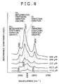
- Fig. 8 is a diagram showing the relation between the concentration of the solution used to form the cast film and the IRA spectrum of the cast film in the high-frequency region.
- Figs. 9A and 9B illustrate the orientation of the alkyl chain adsorbing to the gold electrode.
- Fig. 9A shows the flat-on all-trans configuration in side view and perspective view.
- Fig. 9B shows the gauche configuration in side view and perspective view.
- the flat-on all-trans configuration shown in Fig. 9A is characterized in that methylene groups adjoining to each other along the carbon chain take on the mutually trans configuration, with one hydrogen atom of the methylene group adsorbing to the surface of the substrate, so that the methylene groups orient in one direction.
- Figs. 10A, 10B, and 10C are diagrams illustrating the orientation of the methylene groups (with the alkyl chain taking on the flat-on all-trans configuration) and the relation between the vibration mode and the change in direction of the dipole moment. It is noted that the methylene groups orient such that two hydrogen atoms vertically overlap each other on the surface of the substrate. Therefore, the antisymmetric stretching vibration of CH 2 shown in Fig. 10A causes the dipole moment to change in the direction perpendicular to the surface of the substrate, whereas the symmetric stretching vibration of CH 2 shown in Figs. 10B and 10C causes the dipole moment to change in the direction parallel to the surface of the substrate.
- white arrows indicate the dipole moment that changes in the direction perpendicular to the surface of the substrate and black arrows indicate the dipole moment that changes in the direction parallel to the surface of the substrate.
- the highly sensitive infrared reflection absorption spectroscopy gives an intense peak due to the vibration mode in which the dipole moment changes in the direction perpendicular to the surface of the substrate. Therefore, it gives only absorption peaks due to the antisymmetric stretching vibration of CH 2 but does not give absorption peaks due to the symmetric stretching vibration of CH 2 if the alkyl chain takes on the flat-on all-trans configuration.
- selectivity does not exist if the alkyl chain takes on the gauche configuration in which the orientation of methylene groups has no regularity; in this case, there is no difference between the absorption spectrum due to the antisymmetric stretching vibration of CH 2 and the absorption spectrum due to the symmetric stretching vibration of CH 2 .
- Fig. 11 is a diagram showing the relation between the concentration of the solution used to form the cast film and the IRA spectrum of the cast film (with annealing at 120°C) in the same high-frequency region as in Fig. 8.
- Comparison between Fig. 11 and Fig. 8 reveals that the IRA spectrum changes only little irrespective of the concentration of the solution used.
- the cast film formed from the solution with a concentration of 15.6 ⁇ mol/L merely gave a small absorption peak due to the antisymmetric stretching vibration of CH 2 at 2906 cm -1 .
- Even the cast film (with annealing) formed from the solution with a concentration of 15.6 ⁇ mol/L has the methyl group taking on the gauche configuration. This suggests that annealing changed the structure of the adsorbed alkyl chain.
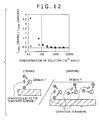
- Fig. 12 is a graph showing how annealing affects the relation between I 2906/ I 2928 and the concentration of the solution used to form the cast film, the former representing the ratio of I 2906 (the absorption intensity of the antisymmetric stretching vibration band at 2906 cm -1 due to flat-on all-trans configuration) to I 2928 (the absorption intensity of the antisymmetric stretching vibration band at 2928 cm -1 due to gauche configuration).
- black points denote the values before annealing and cross marks denote the values after annealing.
- the horizontal solid line represents the values of the transmission absorption spectrum for the bulk substance and the vertical dotted line represents the upper limit of the concentration which presumably forms a molecular monolayer on the gold electrode.
- the cast film without annealing is composed of the first molecular layer (adsorbing to the gold electrode) in which most methylene groups take on the flat-on all-trans configuration and the second and upper molecular layers in which most methylene groups take on the gauche configuration as in the bulk substance. It is also noted that the cast film with annealing is composed of molecular layers in all of which (including the first layer) the gauche configuration dominates as in the bulk substance.
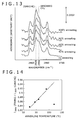
- Fig. 13 is an IRA spectrum which illustrates how the cast film (composed of a little over one molecular layer) formed from the solution with a concentration of 125 ⁇ mol/L varies depending on the annealing temperature in desorption temperature of alkyl chains adsorbing to the substrate.
- Fig. 14 is a diagram showing the relation between I 2906 /I 2928 and the annealing temperature, the former being the ratio of absorption intensity at 2906 cm -1 and 2928 cm -1 in the spectrum shown in Fig. 13.
- the skeleton having the nearly discoid linear tetrapyrrole structure was examined for orientation by noting the absorption spectrum in the medium wavenumber region.
- Figs. 16A, 16B, and 16C show how the cast film varies in IRA spectrum (in the medium frequency region) depending on the concentration the solution from which it is formed (at 250 ⁇ mol/L, 1 mmol/L, and 4 mmol/L).
- Fig. 17 is an infrared transmission absorption spectrum (in the medium frequency region) of the ⁇ -electron conjugated molecule 7 in bulk form.
- the intramolecular association band (b) due to the aromatic ketone shifts toward the high-frequency side more than that of the molecule in bulk as the film thickness decreases, while the intramolecular association band (c) shifts toward the low-frequency side as the film thickness decreases. This suggests that the molecular association of the ⁇ -electron conjugated molecule 7 decreases as the film thickness decreases.
- the area ratio of the absorption intensity of band (a) and band (b) is 1:6 in the case of bulk material, whereas it is 1:3 in the case of the cast film formed from the solution of 4 mmol/L, 1:1 in the case of the cast film formed from the solution of 1 mmol/L, and 1:0.5 in the case of the cast film formed from the solution of 250 ⁇ mol/L.
- the band (e) and the band (f) due to the C-C bond and C-N bond respectively of the pyrrole ring of the thin film shift toward the high-frequency side as compared with those of the bulk material. This suggests an energy increase and consequent distortion of the pyrrole ring.
- the oop band (g) due to the C-H bond of the pyrrole ring does not appear in the case of bulk material, and it becomes more intense as the film thickness decreases.
- Figs. 18A, 18B, and 18C are diagrams showing how the cast film changes in IRA spectrum (in the highest frequency region) depending on the concentration of the solution from which the cast film is formed, with the concentration being at 250 ⁇ mol/L, 1 mmol/L, and 4 mmol/L.
- Fig. 19 is an infrared transmission absorption spectrum of the ⁇ -electron conjugated molecule 7 (in bulk form) in the highest wavenumber region.
- N-H stretching vibration band which is as intense as that in the spectrum for the bulk material, in the spectrum of the cast film formed from the 4 mmol/L solution. This suggests that the lactam ring A orients in various directions. Moreover, the fact that the O-H stretching vibration band shifts toward the high frequency side suggests a decrease in intramolecular association. In the case of the cast film formed from the 1 mmol/L solution, the N-H stretching vibration band is weaker than that in the spectrum of the bulk material, and this suggests the possibility that the lactam ring A orients in a specific direction.
- edge-on orientation with respect to the substrate usually takes place in the case of structure like discotic liquid crystal, which consists of the discoid central part and the alkyl group side chain.
- face-on orientation uniquely occurs on the gold substrate as in this example.
- Gold from which the electrode was made in this example may be replaced by silver or copper if adsorptivity of alkyl chain is taken into adequate consideration.
- This example demonstrates the on-off characteristics of the insulated gate field effect transistor 20 (shown in Fig. 3) in which the ⁇ -electron conjugated molecule is any of those designated as 7 to 9 in Figs. 20A to 20D.
- the same procedure as above was repeated except that the ⁇ -electron conjugated molecule was replaced by 4-pentyl-4'-cyanobiphenyl (5CB for short hereinafter).
- the gap between the source electrode 14 and the drain electrode 15 is about 250 nm (which is equivalent to 200 to 300 molecular layers constituting the array structure 4).
- any of the ⁇ -electron conjugated molecules 7 to 9 in the first molecular layer in contact with the electrodes (at both ends of the array structure 4) orients in the same way as the ⁇ -electron conjugated molecule 7 in the first molecular layer in the first example. It is also considered that the skeleton of any of the ⁇ -electron conjugated molecules 7 to 9 in the intermediate molecular layers (excluding those at both ends) orient in the same way as the skeleton 2 of the ⁇ -electron conjugated molecule 7 in the second and subsequent molecular layers in the first example. Since the ⁇ -electron conjugated molecules 7 to 9 take on configuration similar to discotic liquid crystal, the influence of orientation of the skeleton 2 at both ends spreads over hundreds of molecular layers on account of the ⁇ - ⁇ stacking effect.
- Fig. 20A shows the structural formulas of 5CB
- Fig. 20B shows the structural formulas of the ⁇ -electron conjugated molecules 9
- Fig. 20C shows the structural formulas of the ⁇ -electron conjugated molecules 8
- Fig. 20D shows the structural formulas of the ⁇ -electron conjugated molecules 7.
- the ⁇ -electron conjugated molecule 7 is a zinc complex of biladienone derivative, which was used in the first example.
- the ⁇ -electron conjugated molecule 8 is the same biladienone derivative as the ⁇ -electron conjugated molecule 7 except that it has no zinc ion.
- the ⁇ -electron conjugated molecule 9 is a complex with a zinc ion in which the side chain 3 is a phenyl group without any flexible alkyl chain.
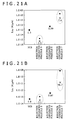
- Figs. 21A and 21B are a diagram showing the change in source-drain current I DS that is observed when the insulated gate field effect transistor 20 is turned on and off by applying a gate voltage to the gate electrode 13.
- Fig. 21A represents the data for a frequency of 0.01 Hz
- Fig. 21B represents the data for a frequency of 0.1 Hz.
- Black points denote the I DS measured without gate voltage
- cross marks denote the I DS measured with gate voltage.
- the insulated gate field effect transistor according to the second example of the present invention operates such that the source-drain current I DS increases to the maximum when no gate voltage is applied but decreases when gate electrode is applied.
- the effect of zinc ion is known from the results attained by the ⁇ -electron conjugated molecules 7 and 8.
- a large source-drain current I DS occurs when no gate electrode is applied.
- the functional molecular element 10 is highly capable of flowing current.
- the source-drain current I DS greatly changes when the gate voltage is turned on and off. This suggests a good switching capability.
- the functional molecular element 10 is poor in ability to flow current and has no switching function regardless of gate voltage turned on and off.
- the effect of alkyl chains in the side chains 3 is known from the results attained by the ⁇ -electron conjugated molecules 7 and 9.
- the functional molecular element 10 is highly capable of flowing current and excels in switching performance in the same way as mentioned above.
- the functional molecular element 10 is poor in ability to flow current, with the source-drain current I DS changing little when gate voltage is turned on and off.
Landscapes
- Chemical & Material Sciences (AREA)
- Engineering & Computer Science (AREA)
- Nanotechnology (AREA)
- Physics & Mathematics (AREA)
- Theoretical Computer Science (AREA)
- Crystallography & Structural Chemistry (AREA)
- Mathematical Physics (AREA)
- Inorganic Chemistry (AREA)
- Materials Engineering (AREA)
- Spectroscopy & Molecular Physics (AREA)
- Thin Film Transistor (AREA)
- Electroluminescent Light Sources (AREA)
- Polyoxymethylene Polymers And Polymers With Carbon-To-Carbon Bonds (AREA)
Applications Claiming Priority (1)
| Application Number | Priority Date | Filing Date | Title |
|---|---|---|---|
| JP2005172629A JP4910314B2 (ja) | 2005-06-13 | 2005-06-13 | 機能性分子素子及び機能性分子装置 |
Publications (2)
| Publication Number | Publication Date |
|---|---|
| EP1734594A2 true EP1734594A2 (fr) | 2006-12-20 |
| EP1734594A3 EP1734594A3 (fr) | 2010-05-26 |
Family
ID=36593819
Family Applications (1)
| Application Number | Title | Priority Date | Filing Date |
|---|---|---|---|
| EP06011764A Withdrawn EP1734594A3 (fr) | 2005-06-13 | 2006-06-07 | Dispostif électronique moléculaire |
Country Status (5)
| Country | Link |
|---|---|
| US (1) | US7629606B2 (fr) |
| EP (1) | EP1734594A3 (fr) |
| JP (1) | JP4910314B2 (fr) |
| KR (1) | KR101236941B1 (fr) |
| CN (1) | CN1881643B (fr) |
Cited By (4)
| Publication number | Priority date | Publication date | Assignee | Title |
|---|---|---|---|---|
| WO2008100461A1 (fr) * | 2007-02-12 | 2008-08-21 | North Carolina State University | Voie de synthèse de porphyrines abcd |
| EP2093815A4 (fr) * | 2006-11-15 | 2011-06-29 | Sony Corp | Élément moléculaire fonctionnel, procédé de production de celui-ci et dispositif moléculaire fonctionnel |
| EP2157604A4 (fr) * | 2007-06-14 | 2011-10-26 | Sony Corp | Élément résistif, élément neuronal, et appareil de traitement d'informations de réseau neuronal |
| US8698132B2 (en) | 2008-06-19 | 2014-04-15 | Sony Corporation | Functional molecular element, manufacturing method thereof, and functional molecular device |
Families Citing this family (12)
| Publication number | Priority date | Publication date | Assignee | Title |
|---|---|---|---|---|
| JP5151122B2 (ja) * | 2006-11-22 | 2013-02-27 | ソニー株式会社 | 電極被覆材料、電極構造体、及び、半導体装置 |
| JP4883796B2 (ja) * | 2007-07-23 | 2012-02-22 | キヤノン株式会社 | 電気化学測定方法 |
| JP5181962B2 (ja) | 2008-09-19 | 2013-04-10 | ソニー株式会社 | 分子素子およびその製造方法ならびに集積回路装置およびその製造方法ならびに三次元集積回路装置およびその製造方法 |
| JP2010080759A (ja) * | 2008-09-26 | 2010-04-08 | Sharp Corp | 有機デバイスとその製造方法 |
| JP5444747B2 (ja) * | 2009-02-17 | 2014-03-19 | ソニー株式会社 | カラー撮像素子およびその製造方法ならびに光センサーおよびその製造方法ならびに光電変換素子およびその製造方法ならびに電子機器 |
| US8723026B2 (en) * | 2009-07-27 | 2014-05-13 | University Of Utah Research Foundation | Parallel coaxial molecular stack arrays |
| US20120186648A1 (en) * | 2009-08-07 | 2012-07-26 | Ling Zang | Coaxial molecular stack for transferring photocurrent generation |
| JP2012209485A (ja) * | 2011-03-30 | 2012-10-25 | Sony Corp | 有機素子の製造方法、有機分子結晶層の接合方法、細線状導電体の製造方法、有機素子および細線状導電体 |
| US9276216B2 (en) * | 2013-09-10 | 2016-03-01 | Kabushiki Kaisha Toshiba | Organic molecular device |
| CN109659356B (zh) * | 2018-12-18 | 2021-08-27 | 河南师范大学 | 基于硒化铜单层的具有负微分电阻和开关作用的纳米器件 |
| JP2023081627A (ja) * | 2021-12-01 | 2023-06-13 | キオクシア株式会社 | 有機分子メモリ |
| CN114213258B (zh) * | 2021-12-13 | 2024-06-18 | 北京未名元上分子技术有限公司 | 一种平面共轭分子化合物及包含其的单分子场效应晶体管 |
Citations (3)
| Publication number | Priority date | Publication date | Assignee | Title |
|---|---|---|---|---|
| WO2003023506A2 (fr) | 2001-09-12 | 2003-03-20 | Cambridge University Technical Services Limited | Cristaux liquides discotiques alignes pour dispositifs |
| US20040201018A1 (en) | 2001-09-05 | 2004-10-14 | Motohiro Yamahara | Polymer structure and functional element having the same, and transistor and display using the same |
| WO2005076379A1 (fr) | 2004-02-10 | 2005-08-18 | Sony Corporation | Element moleculaire fonctionnel |
Family Cites Families (8)
| Publication number | Priority date | Publication date | Assignee | Title |
|---|---|---|---|---|
| JP3524404B2 (ja) * | 1998-10-05 | 2004-05-10 | キヤノン株式会社 | ディスコティック液晶素子および配向方法 |
| US6128214A (en) | 1999-03-29 | 2000-10-03 | Hewlett-Packard | Molecular wire crossbar memory |
| US6256767B1 (en) | 1999-03-29 | 2001-07-03 | Hewlett-Packard Company | Demultiplexer for a molecular wire crossbar network (MWCN DEMUX) |
| WO2000079617A1 (fr) * | 1999-06-21 | 2000-12-28 | Cambridge University Technical Services Limited | Polymeres alignes pour tft organique |
| US6344153B1 (en) * | 1999-08-27 | 2002-02-05 | The Trustees Of Columbia University In The City Of New York | Helical discotic switch |
| JP2002343572A (ja) * | 2001-03-14 | 2002-11-29 | Canon Inc | ポルフィリン誘導体化合物を用いた発光素子および表示装置 |
| JP4247377B2 (ja) * | 2001-12-28 | 2009-04-02 | 独立行政法人産業技術総合研究所 | 薄膜トランジスタ及びその製造方法 |
| JP2005072569A (ja) * | 2003-08-06 | 2005-03-17 | Mitsubishi Chemicals Corp | 有機電界効果トランジスタ |
-
2005
- 2005-06-13 JP JP2005172629A patent/JP4910314B2/ja not_active Expired - Fee Related
-
2006
- 2006-06-06 US US11/422,485 patent/US7629606B2/en not_active Expired - Fee Related
- 2006-06-07 EP EP06011764A patent/EP1734594A3/fr not_active Withdrawn
- 2006-06-08 KR KR1020060051363A patent/KR101236941B1/ko not_active Expired - Fee Related
- 2006-06-12 CN CN2006100913299A patent/CN1881643B/zh not_active Expired - Fee Related
Patent Citations (3)
| Publication number | Priority date | Publication date | Assignee | Title |
|---|---|---|---|---|
| US20040201018A1 (en) | 2001-09-05 | 2004-10-14 | Motohiro Yamahara | Polymer structure and functional element having the same, and transistor and display using the same |
| WO2003023506A2 (fr) | 2001-09-12 | 2003-03-20 | Cambridge University Technical Services Limited | Cristaux liquides discotiques alignes pour dispositifs |
| WO2005076379A1 (fr) | 2004-02-10 | 2005-08-18 | Sony Corporation | Element moleculaire fonctionnel |
Non-Patent Citations (2)
| Title |
|---|
| J. M. WESSELS; H. G. NOTHOFER; W. E. FORD; F. VON WROCHEM; F. SCHOLZ; T. VOSSMEYER; A. SCHROEDTER; H. WELLER; A. YASUDA: "Optical and electrical properties of three-dimensional interlinked gold nanoparticle assemblies", JOURNAL OF THE AMERICAN CHEMICAL SOCIETY, vol. 126, no. 10, 17 March 2004 (2004-03-17), pages 3349 - 3356, XP008048741, DOI: doi:10.1021/ja0377605 |
| M. A. REED; C. ZHOU; C. J. MULLER; T. P. BURGIN; J. M. TOUR: "Conductance of a molecular junction", SCIENCE, vol. 278, 1997, pages 252 - 254, XP000990781, DOI: doi:10.1126/science.278.5336.252 |
Cited By (7)
| Publication number | Priority date | Publication date | Assignee | Title |
|---|---|---|---|---|
| EP2093815A4 (fr) * | 2006-11-15 | 2011-06-29 | Sony Corp | Élément moléculaire fonctionnel, procédé de production de celui-ci et dispositif moléculaire fonctionnel |
| WO2008100461A1 (fr) * | 2007-02-12 | 2008-08-21 | North Carolina State University | Voie de synthèse de porphyrines abcd |
| US7994312B2 (en) | 2007-02-12 | 2011-08-09 | North Carolina State University | Synthetic route to ABCD-porphyrins |
| US8188298B2 (en) | 2007-02-12 | 2012-05-29 | North Carolina State University | Synthetic route to ABCD-porphyrins |
| US8304561B2 (en) | 2007-02-12 | 2012-11-06 | North Carolina State University | Synthetic route to ABCD-porphyrins |
| EP2157604A4 (fr) * | 2007-06-14 | 2011-10-26 | Sony Corp | Élément résistif, élément neuronal, et appareil de traitement d'informations de réseau neuronal |
| US8698132B2 (en) | 2008-06-19 | 2014-04-15 | Sony Corporation | Functional molecular element, manufacturing method thereof, and functional molecular device |
Also Published As
| Publication number | Publication date |
|---|---|
| CN1881643B (zh) | 2010-06-16 |
| KR101236941B1 (ko) | 2013-02-25 |
| CN1881643A (zh) | 2006-12-20 |
| US20060278868A1 (en) | 2006-12-14 |
| KR20060129947A (ko) | 2006-12-18 |
| EP1734594A3 (fr) | 2010-05-26 |
| JP2006351623A (ja) | 2006-12-28 |
| JP4910314B2 (ja) | 2012-04-04 |
| US7629606B2 (en) | 2009-12-08 |
Similar Documents
| Publication | Publication Date | Title |
|---|---|---|
| US7629606B2 (en) | Functional molecular element, method for producing functional molecular element, and functional molecular device | |
| Collier et al. | Molecular-based electronically switchable tunnel junction devices | |
| US7579223B2 (en) | Semiconductor apparatus and process for fabricating the same | |
| Lu et al. | Optimizing the gas sensing properties of sandwich-type phthalocyaninato europium complex through extending the conjugated framework | |
| US8698132B2 (en) | Functional molecular element, manufacturing method thereof, and functional molecular device | |
| US20100244938A1 (en) | Functional molecular element, process for producing the same and functional molecular device | |
| US20090224231A1 (en) | Electronic device, process for producing the same and electronic equipment making use thereof | |
| CN1938875B (zh) | 功能性分子元件 | |
| EP1775782B1 (fr) | Dispositif à molécule fonctionnelle | |
| KR101193581B1 (ko) | 기능성 분자 소자 및 기능성 분자 장치 | |
| Gupta | Photo-switchable molecular wire-based organic electronic devices | |
| James et al. | Self-assembled molecular electronics | |
| US20070159572A1 (en) | Element for modulating area | |
| JP2009032897A (ja) | 機能性分子素子の製造方法及び機能性分子装置の製造方法、並びに集積素子の製造方法 | |
| James et al. | Self-Assembled Molecular | |
| Faramarzi | Light-triggered Molecular Electronics in the 100 Nm Size Range |
Legal Events
| Date | Code | Title | Description |
|---|---|---|---|
| PUAI | Public reference made under article 153(3) epc to a published international application that has entered the european phase |
Free format text: ORIGINAL CODE: 0009012 |
|
| AK | Designated contracting states |
Kind code of ref document: A2 Designated state(s): AT BE BG CH CY CZ DE DK EE ES FI FR GB GR HU IE IS IT LI LT LU LV MC NL PL PT RO SE SI SK TR |
|
| AX | Request for extension of the european patent |
Extension state: AL BA HR MK YU |
|
| PUAL | Search report despatched |
Free format text: ORIGINAL CODE: 0009013 |
|
| AK | Designated contracting states |
Kind code of ref document: A3 Designated state(s): AT BE BG CH CY CZ DE DK EE ES FI FR GB GR HU IE IS IT LI LT LU LV MC NL PL PT RO SE SI SK TR |
|
| AX | Request for extension of the european patent |
Extension state: AL BA HR MK RS |
|
| RIC1 | Information provided on ipc code assigned before grant |
Ipc: G11C 13/02 20060101ALI20100416BHEP Ipc: H01L 51/05 20060101ALI20100416BHEP Ipc: H01L 51/00 20060101AFI20100416BHEP |
|
| 17P | Request for examination filed |
Effective date: 20101126 |
|
| AKX | Designation fees paid |
Designated state(s): DE FR GB |
|
| 17Q | First examination report despatched |
Effective date: 20110316 |
|
| GRAP | Despatch of communication of intention to grant a patent |
Free format text: ORIGINAL CODE: EPIDOSNIGR1 |
|
| RIC1 | Information provided on ipc code assigned before grant |
Ipc: H01L 51/05 20060101ALI20130308BHEP Ipc: H01L 51/30 20060101ALI20130308BHEP Ipc: G11C 13/02 20060101ALI20130308BHEP Ipc: G11C 13/00 20060101ALI20130308BHEP Ipc: H01L 51/00 20060101AFI20130308BHEP |
|
| STAA | Information on the status of an ep patent application or granted ep patent |
Free format text: STATUS: THE APPLICATION IS DEEMED TO BE WITHDRAWN |
|
| 18D | Application deemed to be withdrawn |
Effective date: 20130731 |