EP1737064B1 - Guides d' ondes NRD et systèmes de fond de panier - Google Patents
Guides d' ondes NRD et systèmes de fond de panier Download PDFInfo
- Publication number
- EP1737064B1 EP1737064B1 EP06021041A EP06021041A EP1737064B1 EP 1737064 B1 EP1737064 B1 EP 1737064B1 EP 06021041 A EP06021041 A EP 06021041A EP 06021041 A EP06021041 A EP 06021041A EP 1737064 B1 EP1737064 B1 EP 1737064B1
- Authority
- EP
- European Patent Office
- Prior art keywords
- waveguide
- dielectric
- channel
- bandwidth
- along
- Prior art date
- Legal status (The legal status is an assumption and is not a legal conclusion. Google has not performed a legal analysis and makes no representation as to the accuracy of the status listed.)
- Expired - Lifetime
Links
- 239000000758 substrate Substances 0.000 claims description 5
- 230000005540 biological transmission Effects 0.000 description 9
- 239000004020 conductor Substances 0.000 description 6
- 238000000034 method Methods 0.000 description 6
- 230000007423 decrease Effects 0.000 description 5
- 239000006185 dispersion Substances 0.000 description 3
- 239000004809 Teflon Substances 0.000 description 2
- 229920006362 Teflon® Polymers 0.000 description 2
- 230000008878 coupling Effects 0.000 description 2
- 238000010168 coupling process Methods 0.000 description 2
- 238000005859 coupling reaction Methods 0.000 description 2
- 238000004519 manufacturing process Methods 0.000 description 2
- 239000000463 material Substances 0.000 description 2
- 239000002184 metal Substances 0.000 description 2
- 229910052751 metal Inorganic materials 0.000 description 2
- 150000003071 polychlorinated biphenyls Chemical class 0.000 description 2
- BFKJFAAPBSQJPD-UHFFFAOYSA-N tetrafluoroethene Chemical compound FC(F)=C(F)F BFKJFAAPBSQJPD-UHFFFAOYSA-N 0.000 description 2
- 229910000881 Cu alloy Inorganic materials 0.000 description 1
- 238000011960 computer-aided design Methods 0.000 description 1
- 238000013144 data compression Methods 0.000 description 1
- 230000001419 dependent effect Effects 0.000 description 1
- 239000003989 dielectric material Substances 0.000 description 1
- 230000005670 electromagnetic radiation Effects 0.000 description 1
- 239000003822 epoxy resin Substances 0.000 description 1
- 230000005284 excitation Effects 0.000 description 1
- 239000000835 fiber Substances 0.000 description 1
- 239000011521 glass Substances 0.000 description 1
- 238000003475 lamination Methods 0.000 description 1
- 238000005457 optimization Methods 0.000 description 1
- 230000000737 periodic effect Effects 0.000 description 1
- 229920000647 polyepoxide Polymers 0.000 description 1
- 230000001629 suppression Effects 0.000 description 1
Images




Classifications
-
- H—ELECTRICITY
- H01—ELECTRIC ELEMENTS
- H01P—WAVEGUIDES; RESONATORS, LINES, OR OTHER DEVICES OF THE WAVEGUIDE TYPE
- H01P3/00—Waveguides; Transmission lines of the waveguide type
- H01P3/16—Dielectric waveguides, i.e. without a longitudinal conductor
- H01P3/165—Non-radiating dielectric waveguides
-
- H—ELECTRICITY
- H01—ELECTRIC ELEMENTS
- H01P—WAVEGUIDES; RESONATORS, LINES, OR OTHER DEVICES OF THE WAVEGUIDE TYPE
- H01P1/00—Auxiliary devices
- H01P1/16—Auxiliary devices for mode selection, e.g. mode suppression or mode promotion; for mode conversion
-
- H—ELECTRICITY
- H01—ELECTRIC ELEMENTS
- H01P—WAVEGUIDES; RESONATORS, LINES, OR OTHER DEVICES OF THE WAVEGUIDE TYPE
- H01P3/00—Waveguides; Transmission lines of the waveguide type
- H01P3/12—Hollow waveguides
Definitions
- This invention relates to waveguides and backplane systems according to the pre-amble of claim 1.
- the Shannon-Hartley Theorem provides that, for any given broadband data transmission system protocol, there is usually a linear relationship between the desired system data rate (in Gigabits/sec) and the required system 3dB bandwidth (in Gigahertz). For example, using fiber channel protocol, the available data rate is approximately four times the 3dB system bandwidth. It should be understood that bandwidth considerations related to attenuation are usually referenced to the so-called "3dB bandwidth".
- Traditional broadband data transmission with bandwidth requirements on the order of Gigahertz generally use a data modulated microwave carrier in a "pipe" waveguide as the physical data channel because such waveguides have lower attenuation than comparable cables or PCB's.
- This type of data channel can be thought of as a "broadband microwave modem" data transmission system in comparison to the broadband digital data transmission commonly used on PCB backplane systems.
- the present invention extends conventional, airfilled, rectangular waveguides to a backplane system. These waveguides are described in detail below.
- microwave waveguide structure that can be used as a backplane data channel is the non-radiative dielectric (NRD) waveguide operating in the transverse electric 1,0 (TE 1,0) mode.
- NRD non-radiative dielectric
- the TE 1,0 NRD waveguide structure can be incorporated into a PCB type backplane bus system. This embodiment is also described in detail in below.
- Such broadband microwave modem waveguide backplane systems have superior bandwidth and bandwidth-density characteristics relative to the lowest loss conventional PCB or cable backplane systems.
- QAM quadrature amplitude modulation
- Waveguides have the best transmission characteristics among many transmission lines, because they have no electromagnetic radiation and relatively low attenuation. Waveguides, however, are impractical for circuit boards and packages for two major reasons. First, the size is typically too large for a transmission line to be embedded in circuit boards. Second, waveguides must be surrounded by metal walls. Vertical metal walls cannot be manufactured easily by lamination techniques, a standard fabrication technique for circuit boards or packages.
- Huang J et al "Computer-aided design and optimization of NRD-guide mode suppressors" IEEE Transactions on Microwave Theory and Techniques, IEEE Inc. Vol. 44, No. 6, 1 June 1996, pages 905-910 , as the closest prior art document, discloses a class of nonradiative dielectric waveguide mode suppressors for wideband applications in passive and active NRD integrated circuits.
- the mode suppressors are metallic filter-like pattern elements, based on a technique of controlling out-of-band characteristics of the TEM mode low-pass filter.
- DE-C-750 554 discloses in figure 4 a metallic rectangular waveguide with longitudinal slots in its broad walls.
- NRD waveguide according to the invention is characterized by the characterizing portion of claim 1.
- a backplane system according to the invention comprises a substrate is defined in claim 3.
- the attenuation (A) of a broadside coupled PCB conductor pair data channel has two components: a square root of frequency (f) term due to conductor losses, and a linear term in frequency arising from dielectric losses.
- A A 1 * SQRT f + A 2 * f * L * 8.686 db / neper
- a 1 ⁇ * ⁇ 0 * p 0.5 / w / p * p * Z 0
- a 2 ⁇ * DF * ⁇ 0 * ⁇ 0 0.5 .
- the data channel pitch is p
- w is the trace width
- Z o is the resistivity of the PCB traces
- ⁇ and DF are the permittivity and dissipation factor of the PCB dielectric, respectively.
- w/p is held constant at -0.5 or less
- the solution of Equation (1) for A 3dB yields the 3dB bandwidth of the data channel for a specific backplane length, L.
- SPEEDBOARD TM which is manufactured and distributed by Gore, is an example of a low loss, "TEFLON” laminate.
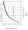
- Figure 1 shows a plot of the bandwidth per channel for a 0.75m “SPEEDBOARD” TM backplane as a function of data channel pitch, as known from 'Metral® high bandwidth - a differential pair connector for applications up to 6 GHz', R.A. Elco, Future digital interconnects over 500 MHz IMAPS Workshop, pages 1-5, January 20-22, 1999 .
- the data channel pitch, p decreases, the channel bandwidth also decreases due to increasing conductor losses relative to the dielectric losses.
- the backplane connector performance can be characterized in terms of the bandwidth vs. bandwidth-density plane, or "phase plane" representation.
- Plots of bandwidth vs. bandwidth density/layer for a 0.5m FR-4 backplane, and for 1.0m and 0.75m “SPEEDBOARD” TM backplanes are shown in Figure 3 , where channel pitch is the independent variable.
- FR-4 is another well-known PCB material, which is a glass reinforced epoxy resin. It is evident that, for a given bandwidth density, there are two possible solutions for channel bandwidth, i.e., a dense low bandwidth "parallel” solution, and a high bandwidth "serial” solution. The limits on bandwidth-density for even high performance PCBs should be clear to those of skill in the art.
- FIG 4A shows a conventional TE mode NRD waveguide 20.
- Waveguide 20 is derived from a rectangular waveguide, partially filled with a dielectric material 22, with the sidewalls removed. As shown, waveguide 20 includes an upper conductive plate 24U, and a lower conductive plate 24L disposed opposite and generally parallel to upper plate 24U.
- Dielectric channel 22 is disposed along a waveguide axis (shown as the z-axis in Figure 4A ) between conductive plates 24U and 24L.
- a second channel 26 is disposed along waveguide axis 30 adjacent to dielectric channel 22.
- US-A 5,473,296 describes the manufacture of NRD waveguides.
- Waveguide 20 can support both an even and an odd longitudinal magnetic mode (relative to the symmetry of the magnetic field in the direction of propagation).
- the even mode has a cutoff frequency, while the odd mode does not.
- the field patterns in waveguide 20 for the desired odd mode are shown in Figure 4B .
- the fields in dielectric 22 are similar to those of the TE 1,0 mode in rectangular waveguide 10 described above, and vary as E y ⁇ cos(kx) and H z ⁇ sin(kx). Outside of dielectric 22, however, the fields decay exponentially with x, i.e., exp(- ⁇ x), because of the reactive loading of the air spaces on the left and right faces 22L, 22R of dielectric 22.
- the range of operation is for values of F between 1 and 2 where there is only moderate dispersion.
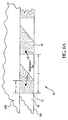
- NRD waveguides 30 can be laminated between substrates 24U, 24L, such as ground plane PCBs, to form a periodic multiple bus structure as illustrated in Figure 6A .
- the first order consequence of the coupling of the fields external to dielectric 22 is some level of crosstalk between the dielectric waveguides 30. This coupling decreases with increasing pitch, p, and normalized frequency, F, as illustrated in Figure 7 . Therefore, the acceptable crosstalk levels determine the minimum waveguide pitch pmin.
- Waveguide backplane system 120 includes an upper conductive plate 124U, and a lower conductive plate 124L disposed opposite and generally parallel to upper plate 124U.
- plates 124U and 124L are made from a suitable conducting material, such as a copper alloy, and are grounded.
- a dielectric channel 122 is disposed along a waveguide axis 130 between conducive plates 124U and 124L. Gaps 128 in the conductive plates are formed along waveguide axis 130. Gaps 128 are disposed near the middle of each dielectric channel 122. An air-filled channel 126 is disposed along waveguide axis 130 adjacent to dielectric channel 122.
- waveguide 120 can include a plurality of dielectric channels 122 separated by air-filled channels 126. Dielectric channels 122 could be made from any suitable material.
- the bandwidth of the TE 1,0 mode NRD waveguide is dependent on the losses in dielectric and the conducting ground planes.
- the attenuation has two components: a linear term in frequency proportional to the dielectric loss tangent, and a 3/2 power term in frequency due to losses in the conducting ground planes.
Landscapes
- Waveguides (AREA)
- Physical Or Chemical Processes And Apparatus (AREA)
- Crystals, And After-Treatments Of Crystals (AREA)
Claims (6)
- Guide d'onde diélectrique non rayonnant comprenant :une première plaque conductrice (124U) ;une seconde plaque conductrice placée en parallèle (124L) ;au moins un canal diélectrique (122) disposé le long d'un axe de guide d'onde (130) entre les plaques conductrices (124U, 124L) ;un second canal (126) rempli d'air disposé le long de l'axe de guide d'onde (130) adjacent au canal diélectrique (122) entre les plaques conductrices (124U, 124L) et un élément de suppression de mode, caractérisé en ce que l'élément de suppression de mode est adapté de telle sorte que la première plaque conductrice (124U) comporte au moins un espace (128) le long de l'axe de guide d'onde (130), le au moins un espace (128) étant positionné au-dessus du au moins un canal diélectrique (122) et ayant une largeur d'espace qui permet une propagation le long de l'axe de guide d'onde (130) d'ondes électromagnétiques dans un mode magnétique longitudinal impair, mais supprime des ondes électromagnétiques dans un mode magnétique longitudinal pair, etle au moins un espace (128) est disposé près du milieu dudit au moins un canal diélectrique (122).
- Guide d'onde selon la revendication 1, dans lequel le canal diélectrique (122) a une section transversale généralement rectangulaire le long de l'axe de guide d'onde (130).
- Système de fond panier (120) de guide d'onde diélectrique non rayonnant (NRD - pour Non Radiative Dielectric) comprenant :un substrat ;un guide d'onde diélectrique non rayonnant selon au moins l'une des revendications 1 à 3, connecté au substrat ;au moins un émetteur connecté au guide d'onde diélectrique non rayonnant pour envoyer un signal électrique le long du guide d'onde ; etau moins un récepteur connecté au guide d'onde pour recevoir le signal électrique.
- Système de fond de panier (120) selon la revendication 3, dans lequel le substrat est une carte multicouche.
- Système de fond de panier (120) selon au moins l'une des revendications 3 et 4, dans lequel l'émetteur et le récepteur sont des émetteurs-récepteurs.
- Système de fond de panier (120) selon la revendication 5, dans lequel les émetteurs-récepteurs sont des modems à micro-ondes à largeur de bande du gigahertz.
Applications Claiming Priority (2)
| Application Number | Priority Date | Filing Date | Title |
|---|---|---|---|
| US09/429,812 US6590477B1 (en) | 1999-10-29 | 1999-10-29 | Waveguides and backplane systems with at least one mode suppression gap |
| EP00123315A EP1096596A3 (fr) | 1999-10-29 | 2000-10-26 | Guides d' ondes et systèmes de fond de panier |
Related Parent Applications (1)
| Application Number | Title | Priority Date | Filing Date |
|---|---|---|---|
| EP00123315A Division EP1096596A3 (fr) | 1999-10-29 | 2000-10-26 | Guides d' ondes et systèmes de fond de panier |
Publications (2)
| Publication Number | Publication Date |
|---|---|
| EP1737064A1 EP1737064A1 (fr) | 2006-12-27 |
| EP1737064B1 true EP1737064B1 (fr) | 2008-04-09 |
Family
ID=23704833
Family Applications (2)
| Application Number | Title | Priority Date | Filing Date |
|---|---|---|---|
| EP06021041A Expired - Lifetime EP1737064B1 (fr) | 1999-10-29 | 2000-10-26 | Guides d' ondes NRD et systèmes de fond de panier |
| EP00123315A Withdrawn EP1096596A3 (fr) | 1999-10-29 | 2000-10-26 | Guides d' ondes et systèmes de fond de panier |
Family Applications After (1)
| Application Number | Title | Priority Date | Filing Date |
|---|---|---|---|
| EP00123315A Withdrawn EP1096596A3 (fr) | 1999-10-29 | 2000-10-26 | Guides d' ondes et systèmes de fond de panier |
Country Status (6)
| Country | Link |
|---|---|
| US (3) | US6590477B1 (fr) |
| EP (2) | EP1737064B1 (fr) |
| JP (1) | JP2001189610A (fr) |
| AT (1) | ATE392023T1 (fr) |
| CA (1) | CA2324570A1 (fr) |
| DE (1) | DE60038586T2 (fr) |
Families Citing this family (67)
| Publication number | Priority date | Publication date | Assignee | Title |
|---|---|---|---|---|
| FI113581B (fi) * | 1999-07-09 | 2004-05-14 | Nokia Corp | Menetelmä aaltojohdon toteuttamiseksi monikerroskeramiikkarakenteissa ja aaltojohto |
| US6590477B1 (en) * | 1999-10-29 | 2003-07-08 | Fci Americas Technology, Inc. | Waveguides and backplane systems with at least one mode suppression gap |
| US20070268087A9 (en) * | 2000-11-03 | 2007-11-22 | Lemke Timothy A | High speed, controlled impedance air dielectric electronic backplane systems |
| US7088199B2 (en) * | 2004-05-28 | 2006-08-08 | International Business Machines Corporation | Method and stiffener-embedded waveguide structure for implementing enhanced data transfer |
| JP4337779B2 (ja) * | 2004-07-01 | 2009-09-30 | ソニー株式会社 | 物理情報取得方法および物理情報取得装置並びに物理量分布検知の半導体装置 |
| US7271680B2 (en) * | 2005-06-29 | 2007-09-18 | Intel Corporation | Method, apparatus, and system for parallel plate mode radial pattern signaling |
| US7301424B2 (en) * | 2005-06-29 | 2007-11-27 | Intel Corporation | Flexible waveguide cable with a dielectric core |
| US7551042B1 (en) * | 2006-06-09 | 2009-06-23 | Johnson Ray M | Microwave pulse compressor using switched oversized waveguide resonator |
| US8032089B2 (en) * | 2006-12-30 | 2011-10-04 | Broadcom Corporation | Integrated circuit/printed circuit board substrate structure and communications |
| US9136570B2 (en) * | 2007-12-07 | 2015-09-15 | K & L Microwave, Inc. | High Q surface mount technology cavity filter |
| JP4645664B2 (ja) * | 2008-03-06 | 2011-03-09 | 株式会社デンソー | 高周波装置 |
| US8274147B2 (en) * | 2008-06-19 | 2012-09-25 | Broadcom Corporation | Method and system for intra-printed circuit board communication via waveguides |
| US9322904B2 (en) | 2011-06-15 | 2016-04-26 | Keyssa, Inc. | Proximity sensing using EHF signals |
| US9407311B2 (en) | 2011-10-21 | 2016-08-02 | Keyssa, Inc. | Contactless signal splicing using an extremely high frequency (EHF) communication link |
| US8554136B2 (en) | 2008-12-23 | 2013-10-08 | Waveconnex, Inc. | Tightly-coupled near-field communication-link connector-replacement chips |
| JP2011044953A (ja) * | 2009-08-21 | 2011-03-03 | Sony Corp | Av機器用の有線伝送線路 |
| US8730314B2 (en) * | 2010-04-13 | 2014-05-20 | Varian Medical Systems, Inc. | Systems and methods for monitoring radiation treatment |
| KR101582395B1 (ko) | 2011-03-24 | 2016-01-11 | 키사, 아이엔씨. | 전자기 통신의 집적회로 |
| US8811526B2 (en) | 2011-05-31 | 2014-08-19 | Keyssa, Inc. | Delta modulated low power EHF communication link |
| US9372214B2 (en) * | 2011-06-03 | 2016-06-21 | Cascade Microtech, Inc. | High frequency interconnect structures, electronic assemblies that utilize high frequency interconnect structures, and methods of operating the same |
| US20130278360A1 (en) * | 2011-07-05 | 2013-10-24 | Waveconnex, Inc. | Dielectric conduits for ehf communications |
| TWI595715B (zh) | 2012-08-10 | 2017-08-11 | 奇沙公司 | 用於極高頻通訊之介電耦接系統 |
| US9478840B2 (en) * | 2012-08-24 | 2016-10-25 | City University Of Hong Kong | Transmission line and methods for fabricating thereof |
| CN104769852B (zh) | 2012-09-14 | 2016-09-21 | 凯萨股份有限公司 | 具有虚拟磁滞的无线连接 |
| CN104937769B (zh) | 2012-12-17 | 2018-11-16 | 凯萨股份有限公司 | 模块化电子设备 |
| WO2014145366A2 (fr) | 2013-03-15 | 2014-09-18 | Keyssa, Inc. | Puce de communication à extrêmement haute fréquence |
| EP2974504B1 (fr) | 2013-03-15 | 2018-06-20 | Keyssa, Inc. | Dispositif de communication sécurisé ehf |
| US9793603B2 (en) * | 2013-06-27 | 2017-10-17 | Hewlett Packard Enterprise Development Lp | Millimeter wave frequency data communication systems |
| US9548523B2 (en) | 2014-04-09 | 2017-01-17 | Texas Instruments Incorporated | Waveguide formed with a dielectric core surrounded by conductive layers including a conformal base layer that matches the footprint of the waveguide |
| US9769446B1 (en) * | 2015-03-10 | 2017-09-19 | Lentix, Inc. | Digital image dynamic range processing apparatus and method |
| US10411320B2 (en) | 2015-04-21 | 2019-09-10 | 3M Innovative Properties Company | Communication devices and systems with coupling device and waveguide |
| CN107534199B (zh) * | 2015-04-21 | 2022-06-17 | 3M创新有限公司 | 具有高电介质谐振器的波导 |
| US10240947B2 (en) * | 2015-08-24 | 2019-03-26 | Apple Inc. | Conductive cladding for waveguides |
| US10170831B2 (en) * | 2015-08-25 | 2019-01-01 | Elwha Llc | Systems, methods and devices for mechanically producing patterns of electromagnetic energy |
| US20180310399A1 (en) * | 2015-12-21 | 2018-10-25 | Intel Corporation | Microelectronic devices with embedded substrate cavities for device to device communications |
| CN113507293B (zh) | 2016-02-01 | 2023-09-05 | 安费诺富加宜(亚洲)私人有限公司 | 高速数据通信系统 |
| WO2018063342A1 (fr) * | 2016-09-30 | 2018-04-05 | Rawlings Brandon M | Co-extrusion d'ensembles en multiples matériaux pour la fabrication de guide d'ondes à ondes millimétriques |
| US10587026B2 (en) * | 2017-01-27 | 2020-03-10 | The Government Of The United States Of America, As Represented By The Secretary Of The Navy | Fully integrated broadband interconnect |
| US10468736B2 (en) | 2017-02-08 | 2019-11-05 | Aptiv Technologies Limited | Radar assembly with ultra wide band waveguide to substrate integrated waveguide transition |
| US10584580B2 (en) | 2017-10-23 | 2020-03-10 | SharpKeen Enterprises, Inc. | Electromagnetic surface wave communication in a pipe |
| US11527808B2 (en) | 2019-04-29 | 2022-12-13 | Aptiv Technologies Limited | Waveguide launcher |
| US11362436B2 (en) | 2020-10-02 | 2022-06-14 | Aptiv Technologies Limited | Plastic air-waveguide antenna with conductive particles |
| US11757166B2 (en) | 2020-11-10 | 2023-09-12 | Aptiv Technologies Limited | Surface-mount waveguide for vertical transitions of a printed circuit board |
| US11681015B2 (en) | 2020-12-18 | 2023-06-20 | Aptiv Technologies Limited | Waveguide with squint alteration |
| US11626668B2 (en) | 2020-12-18 | 2023-04-11 | Aptiv Technologies Limited | Waveguide end array antenna to reduce grating lobes and cross-polarization |
| US11749883B2 (en) | 2020-12-18 | 2023-09-05 | Aptiv Technologies Limited | Waveguide with radiation slots and parasitic elements for asymmetrical coverage |
| US11901601B2 (en) | 2020-12-18 | 2024-02-13 | Aptiv Technologies Limited | Waveguide with a zigzag for suppressing grating lobes |
| US11502420B2 (en) | 2020-12-18 | 2022-11-15 | Aptiv Technologies Limited | Twin line fed dipole array antenna |
| US11444364B2 (en) | 2020-12-22 | 2022-09-13 | Aptiv Technologies Limited | Folded waveguide for antenna |
| US11668787B2 (en) | 2021-01-29 | 2023-06-06 | Aptiv Technologies Limited | Waveguide with lobe suppression |
| US12058804B2 (en) | 2021-02-09 | 2024-08-06 | Aptiv Technologies AG | Formed waveguide antennas of a radar assembly |
| US11721905B2 (en) | 2021-03-16 | 2023-08-08 | Aptiv Technologies Limited | Waveguide with a beam-forming feature with radiation slots |
| US11616306B2 (en) | 2021-03-22 | 2023-03-28 | Aptiv Technologies Limited | Apparatus, method and system comprising an air waveguide antenna having a single layer material with air channels therein which is interfaced with a circuit board |
| EP4084222A1 (fr) | 2021-04-30 | 2022-11-02 | Aptiv Technologies Limited | Guide d'ondes à charge diélectrique pour les distributions de signaux à faibles pertes et les antennes à petit facteur de forme |
| US11973268B2 (en) | 2021-05-03 | 2024-04-30 | Aptiv Technologies AG | Multi-layered air waveguide antenna with layer-to-layer connections |
| US11962085B2 (en) | 2021-05-13 | 2024-04-16 | Aptiv Technologies AG | Two-part folded waveguide having a sinusoidal shape channel including horn shape radiating slots formed therein which are spaced apart by one-half wavelength |
| US11616282B2 (en) | 2021-08-03 | 2023-03-28 | Aptiv Technologies Limited | Transition between a single-ended port and differential ports having stubs that match with input impedances of the single-ended and differential ports |
| US12224502B2 (en) | 2021-10-14 | 2025-02-11 | Aptiv Technologies AG | Antenna-to-printed circuit board transition |
| US12456816B2 (en) | 2022-05-02 | 2025-10-28 | Aptiv Technologies AG | Waveguide with slot antennas and reflectors |
| US12265172B2 (en) * | 2022-05-25 | 2025-04-01 | Aptiv Technologies AG | Vertical microstrip-to-waveguide transition |
| US12315999B2 (en) | 2022-07-15 | 2025-05-27 | Aptiv Technologies AG | Solderable waveguide antenna |
| US12424767B2 (en) | 2022-11-15 | 2025-09-23 | Aptiv Technologies AG | Planar surface features for waveguide and antenna |
| US12537308B2 (en) | 2023-01-24 | 2026-01-27 | Aptiv Technologies AG | Symmetrical two-piece waveguide |
| US12148992B2 (en) | 2023-01-25 | 2024-11-19 | Aptiv Technologies AG | Hybrid horn waveguide antenna |
| JP7719117B2 (ja) * | 2023-04-14 | 2025-08-05 | アンリツ株式会社 | マルチプレクサ、これを用いるスペクトラムアナライザ、シグナルアナライザ、信号発生装置、及びマルチプレクサの制御方法 |
| US12506272B2 (en) | 2023-05-16 | 2025-12-23 | Aptiv Technologies AG | Production-tolerant multi-part antenna system |
| US12627020B2 (en) | 2023-05-18 | 2026-05-12 | Aptiv Technologies AG | Waveguide with a curved-wall low-pass filter |
Family Cites Families (36)
| Publication number | Priority date | Publication date | Assignee | Title |
|---|---|---|---|---|
| DE750554C (de) | 1940-10-31 | 1945-01-17 | Hohlrohrleitung zur dielektrischen Fortleitung kurzer elektromagnetischer Wellen | |
| DE893819C (de) * | 1944-12-23 | 1953-10-19 | Siemens Ag | Hohlrohrleitung |
| US3157847A (en) * | 1961-07-11 | 1964-11-17 | Robert M Williams | Multilayered waveguide circuitry formed by stacking plates having surface grooves |
| DE1158597B (de) * | 1962-02-23 | 1963-12-05 | Telefunken Patent | Verlustarmer Hohlleiter zur UEbertragung der H-Welle |
| DE1275649B (de) * | 1963-06-08 | 1968-08-22 | Sumitomo Electric Industries | Seitlich offener Hohlleiter fuer die UEbertragung elektromagnetischer Oberflaechenwellen |
| US3315187A (en) | 1966-01-25 | 1967-04-18 | Sumitomo Electric Industries | Microwave transmission line |
| GB1320673A (en) | 1971-01-12 | 1973-06-20 | Cambridge Scientific Instr Ltd | Microwave spectroscopy |
| US3686590A (en) | 1971-06-24 | 1972-08-22 | Rca Corp | Sheet metal waveguide constructed of a pair of interlocking sheet metal channels |
| US4001733A (en) | 1975-08-18 | 1977-01-04 | Raytheon Company | Ferrite phase shifter having conductive material plated around ferrite assembly |
| US4156907A (en) | 1977-03-02 | 1979-05-29 | Burroughs Corporation | Data communications subsystem |
| US4200930A (en) | 1977-05-23 | 1980-04-29 | Burroughs Corporation | Adapter cluster module for data communications subsystem |
| US4292669A (en) | 1978-02-28 | 1981-09-29 | Burroughs Corporation | Autonomous data communications subsystem |
| GB2119581A (en) | 1982-04-26 | 1983-11-16 | Philips Electronic Associated | Waveguide/microstrip mode transducer |
| US4587651A (en) | 1983-05-04 | 1986-05-06 | Cxc Corporation | Distributed variable bandwidth switch for voice, data, and image communications |
| US4677404A (en) * | 1984-12-19 | 1987-06-30 | Martin Marietta Corporation | Compound dielectric multi-conductor transmission line |
| US4800350A (en) * | 1985-05-23 | 1989-01-24 | The United States Of America As Represented By The Secretary Of The Navy | Dielectric waveguide using powdered material |
| US4818963A (en) | 1985-06-05 | 1989-04-04 | Raytheon Company | Dielectric waveguide phase shifter |
| US4862186A (en) | 1986-11-12 | 1989-08-29 | Hughes Aircraft Company | Microwave antenna array waveguide assembly |
| US4777657A (en) | 1987-04-01 | 1988-10-11 | Iss Engineering, Inc. | Computer controlled broadband receiver |
| GB2222489B (en) | 1988-08-31 | 1992-08-12 | Marconi Electronic Devices | Waveguide apparatus |
| US5004993A (en) | 1989-09-19 | 1991-04-02 | The United States Of America As Represented By The Secretary Of The Navy | Constricted split block waveguide low pass filter with printed circuit filter substrate |
| US5359714A (en) | 1992-01-06 | 1994-10-25 | Nicolas Avaneas | Avan computer backplane-a redundant, unidirectional bus architecture |
| US5398010A (en) * | 1992-05-07 | 1995-03-14 | Hughes Aircraft Company | Molded waveguide components having electroless plated thermoplastic members |
| FR2700069B1 (fr) | 1992-12-24 | 1995-03-17 | Adv Comp Res Inst Sarl | Système d'interconnexion de cartes d'un système informatique rapide. |
| JP3123293B2 (ja) | 1993-03-05 | 2001-01-09 | 株式会社村田製作所 | 非放射性誘電体線路およびその製造方法 |
| EP0618642B1 (fr) | 1993-03-31 | 2001-09-19 | Hitachi Kokusai Electric Inc. | Radiateur électromagnétique pour radiation et réception d ondes électromagnétiques |
| US5363464A (en) | 1993-06-28 | 1994-11-08 | Tangible Domain Inc. | Dielectric/conductive waveguide |
| US5818385A (en) | 1994-06-10 | 1998-10-06 | Bartholomew; Darin E. | Antenna system and method |
| US5825268A (en) | 1994-08-30 | 1998-10-20 | Murata Manufacturing Co., Ltd. | Device with a nonradiative dielectric waveguide |
| US5986527A (en) * | 1995-03-28 | 1999-11-16 | Murata Manufacturing Co., Ltd. | Planar dielectric line and integrated circuit using the same line |
| JP3166897B2 (ja) | 1995-08-18 | 2001-05-14 | 株式会社村田製作所 | 非放射性誘電体線路およびその集積回路 |
| US5889449A (en) * | 1995-12-07 | 1999-03-30 | Space Systems/Loral, Inc. | Electromagnetic transmission line elements having a boundary between materials of high and low dielectric constants |
| US5637521A (en) | 1996-06-14 | 1997-06-10 | The United States Of America As Represented By The Secretary Of The Army | Method of fabricating an air-filled waveguide on a semiconductor body |
| US5929728A (en) * | 1997-06-25 | 1999-07-27 | Hewlett-Packard Company | Imbedded waveguide structures for a microwave circuit package |
| JP2001075051A (ja) | 1999-09-03 | 2001-03-23 | Moritex Corp | 不連続多波長光発生装置とこれを用いた偏波分散測定方法 |
| US6590477B1 (en) * | 1999-10-29 | 2003-07-08 | Fci Americas Technology, Inc. | Waveguides and backplane systems with at least one mode suppression gap |
-
1999
- 1999-10-29 US US09/429,812 patent/US6590477B1/en not_active Expired - Lifetime
-
2000
- 2000-10-26 DE DE60038586T patent/DE60038586T2/de not_active Expired - Lifetime
- 2000-10-26 EP EP06021041A patent/EP1737064B1/fr not_active Expired - Lifetime
- 2000-10-26 CA CA002324570A patent/CA2324570A1/fr not_active Abandoned
- 2000-10-26 AT AT06021041T patent/ATE392023T1/de not_active IP Right Cessation
- 2000-10-26 EP EP00123315A patent/EP1096596A3/fr not_active Withdrawn
- 2000-10-30 JP JP2000331135A patent/JP2001189610A/ja active Pending
-
2001
- 2001-10-12 US US09/976,946 patent/US6724281B2/en not_active Expired - Lifetime
-
2004
- 2004-02-18 US US10/780,835 patent/US6960970B2/en not_active Expired - Fee Related
Also Published As
| Publication number | Publication date |
|---|---|
| CA2324570A1 (fr) | 2001-04-29 |
| US20020021197A1 (en) | 2002-02-21 |
| EP1096596A3 (fr) | 2002-12-11 |
| EP1096596A2 (fr) | 2001-05-02 |
| EP1737064A1 (fr) | 2006-12-27 |
| DE60038586D1 (de) | 2008-05-21 |
| ATE392023T1 (de) | 2008-04-15 |
| US6724281B2 (en) | 2004-04-20 |
| US6590477B1 (en) | 2003-07-08 |
| US6960970B2 (en) | 2005-11-01 |
| DE60038586T2 (de) | 2009-06-25 |
| US20040160294A1 (en) | 2004-08-19 |
| JP2001189610A (ja) | 2001-07-10 |
Similar Documents
| Publication | Publication Date | Title |
|---|---|---|
| EP1737064A1 (fr) | Guides d' ondes NRD et systèmes de fond de panier | |
| US11936111B2 (en) | Antenna array based on one or more metamaterial structures | |
| EP2311134B1 (fr) | Guide d'ondes et lignes de transmission dans des interstices entre des surfaces conductrices parallèles | |
| US6614325B1 (en) | RF/IF signal distribution network utilizing broadside coupled stripline | |
| US6535088B1 (en) | Suspended transmission line and method | |
| US7215007B2 (en) | Circuit and method for suppression of electromagnetic coupling and switching noise in multilayer printed circuit boards | |
| EP0883328B1 (fr) | Plaquette de circuits comprenant une ligne de transmission à haute fréquence | |
| Ponchak et al. | The use of metal filled via holes for improving isolation in LTCC RF and wireless multichip packages | |
| CN108206318B (zh) | 印制电路板、光模块、以及光传输装置 | |
| EP1940205A2 (fr) | Carte de circuit à micro-ondes | |
| US11234326B2 (en) | Printed circuit board, optical module, and optical transmission equipment | |
| US10879575B2 (en) | Embedded filtering in PCB integrated ultra high speed dielectric waveguides using photonic band gap structures | |
| EP3879640B1 (fr) | Connecteur coaxial et substrat équipé d'un connecteur coaxial | |
| US6518844B1 (en) | Suspended transmission line with embedded amplifier | |
| CA1316228C (fr) | Coupleur de guides d'ondes multiplan | |
| EP4125152B1 (fr) | Ensemble d'interconnexion bimode entre des circuits intégrés de radiofréquence et un guide d'ondes en plastique | |
| US6552635B1 (en) | Integrated broadside conductor for suspended transmission line and method | |
| US11792915B2 (en) | Printed circuit board and optical transceiver | |
| EP1376740B1 (fr) | Circuit à trois portes de rendement élevé | |
| CN114552155B (zh) | 双模传输线 | |
| CN122026044A (zh) | 一种平面集成空心矩形介质波导 | |
| CN120637837A (zh) | 波导-微带混合集成的低成本低插损差分传输线设计方法 | |
| WO2001080348A1 (fr) | Ligne de transmission suspendue et procede associe | |
| CN112490608A (zh) | 传输组件 | |
| Đorđević | Internal electromagnetic compatibility of RF devices |
Legal Events
| Date | Code | Title | Description |
|---|---|---|---|
| PUAI | Public reference made under article 153(3) epc to a published international application that has entered the european phase |
Free format text: ORIGINAL CODE: 0009012 |
|
| AC | Divisional application: reference to earlier application |
Ref document number: 1096596 Country of ref document: EP Kind code of ref document: P |
|
| AK | Designated contracting states |
Kind code of ref document: A1 Designated state(s): AT BE CH CY DE DK ES FI FR GB GR IE IT LI LU MC NL PT SE |
|
| AX | Request for extension of the european patent |
Extension state: AL LT LV MK RO SI |
|
| 17P | Request for examination filed |
Effective date: 20070627 |
|
| 17Q | First examination report despatched |
Effective date: 20070806 |
|
| AKX | Designation fees paid |
Designated state(s): AT BE CH CY DE DK ES FI FR GB GR IE IT LI LU MC NL PT SE |
|
| GRAP | Despatch of communication of intention to grant a patent |
Free format text: ORIGINAL CODE: EPIDOSNIGR1 |
|
| GRAS | Grant fee paid |
Free format text: ORIGINAL CODE: EPIDOSNIGR3 |
|
| GRAA | (expected) grant |
Free format text: ORIGINAL CODE: 0009210 |
|
| RAP1 | Party data changed (applicant data changed or rights of an application transferred) |
Owner name: FCI |
|
| AC | Divisional application: reference to earlier application |
Ref document number: 1096596 Country of ref document: EP Kind code of ref document: P |
|
| AK | Designated contracting states |
Kind code of ref document: B1 Designated state(s): AT BE CH CY DE DK ES FI FR GB GR IE IT LI LU MC NL PT SE |
|
| REG | Reference to a national code |
Ref country code: GB Ref legal event code: FG4D |
|
| REG | Reference to a national code |
Ref country code: CH Ref legal event code: EP |
|
| REG | Reference to a national code |
Ref country code: IE Ref legal event code: FG4D |
|
| REF | Corresponds to: |
Ref document number: 60038586 Country of ref document: DE Date of ref document: 20080521 Kind code of ref document: P |
|
| NLV1 | Nl: lapsed or annulled due to failure to fulfill the requirements of art. 29p and 29m of the patents act | ||
| PG25 | Lapsed in a contracting state [announced via postgrant information from national office to epo] |
Ref country code: ES Free format text: LAPSE BECAUSE OF FAILURE TO SUBMIT A TRANSLATION OF THE DESCRIPTION OR TO PAY THE FEE WITHIN THE PRESCRIBED TIME-LIMIT Effective date: 20080720 Ref country code: NL Free format text: LAPSE BECAUSE OF FAILURE TO SUBMIT A TRANSLATION OF THE DESCRIPTION OR TO PAY THE FEE WITHIN THE PRESCRIBED TIME-LIMIT Effective date: 20080409 Ref country code: PT Free format text: LAPSE BECAUSE OF FAILURE TO SUBMIT A TRANSLATION OF THE DESCRIPTION OR TO PAY THE FEE WITHIN THE PRESCRIBED TIME-LIMIT Effective date: 20080910 |
|
| PG25 | Lapsed in a contracting state [announced via postgrant information from national office to epo] |
Ref country code: AT Free format text: LAPSE BECAUSE OF FAILURE TO SUBMIT A TRANSLATION OF THE DESCRIPTION OR TO PAY THE FEE WITHIN THE PRESCRIBED TIME-LIMIT Effective date: 20080409 |
|
| ET | Fr: translation filed | ||
| PG25 | Lapsed in a contracting state [announced via postgrant information from national office to epo] |
Ref country code: SE Free format text: LAPSE BECAUSE OF FAILURE TO SUBMIT A TRANSLATION OF THE DESCRIPTION OR TO PAY THE FEE WITHIN THE PRESCRIBED TIME-LIMIT Effective date: 20080709 Ref country code: DK Free format text: LAPSE BECAUSE OF FAILURE TO SUBMIT A TRANSLATION OF THE DESCRIPTION OR TO PAY THE FEE WITHIN THE PRESCRIBED TIME-LIMIT Effective date: 20080409 |
|
| PLBE | No opposition filed within time limit |
Free format text: ORIGINAL CODE: 0009261 |
|
| STAA | Information on the status of an ep patent application or granted ep patent |
Free format text: STATUS: NO OPPOSITION FILED WITHIN TIME LIMIT |
|
| PG25 | Lapsed in a contracting state [announced via postgrant information from national office to epo] |
Ref country code: BE Free format text: LAPSE BECAUSE OF FAILURE TO SUBMIT A TRANSLATION OF THE DESCRIPTION OR TO PAY THE FEE WITHIN THE PRESCRIBED TIME-LIMIT Effective date: 20080409 |
|
| 26N | No opposition filed |
Effective date: 20090112 |
|
| PG25 | Lapsed in a contracting state [announced via postgrant information from national office to epo] |
Ref country code: MC Free format text: LAPSE BECAUSE OF NON-PAYMENT OF DUE FEES Effective date: 20081031 |
|
| REG | Reference to a national code |
Ref country code: CH Ref legal event code: PL |
|
| GBPC | Gb: european patent ceased through non-payment of renewal fee |
Effective date: 20081026 |
|
| REG | Reference to a national code |
Ref country code: FR Ref legal event code: ST Effective date: 20090630 |
|
| PG25 | Lapsed in a contracting state [announced via postgrant information from national office to epo] |
Ref country code: IT Free format text: LAPSE BECAUSE OF FAILURE TO SUBMIT A TRANSLATION OF THE DESCRIPTION OR TO PAY THE FEE WITHIN THE PRESCRIBED TIME-LIMIT Effective date: 20080409 |
|
| PG25 | Lapsed in a contracting state [announced via postgrant information from national office to epo] |
Ref country code: CY Free format text: LAPSE BECAUSE OF FAILURE TO SUBMIT A TRANSLATION OF THE DESCRIPTION OR TO PAY THE FEE WITHIN THE PRESCRIBED TIME-LIMIT Effective date: 20080409 |
|
| PG25 | Lapsed in a contracting state [announced via postgrant information from national office to epo] |
Ref country code: CH Free format text: LAPSE BECAUSE OF NON-PAYMENT OF DUE FEES Effective date: 20081031 Ref country code: FR Free format text: LAPSE BECAUSE OF NON-PAYMENT OF DUE FEES Effective date: 20081031 Ref country code: LI Free format text: LAPSE BECAUSE OF NON-PAYMENT OF DUE FEES Effective date: 20081031 Ref country code: IE Free format text: LAPSE BECAUSE OF NON-PAYMENT OF DUE FEES Effective date: 20081028 |
|
| PG25 | Lapsed in a contracting state [announced via postgrant information from national office to epo] |
Ref country code: GB Free format text: LAPSE BECAUSE OF NON-PAYMENT OF DUE FEES Effective date: 20081026 |
|
| PG25 | Lapsed in a contracting state [announced via postgrant information from national office to epo] |
Ref country code: FI Free format text: LAPSE BECAUSE OF FAILURE TO SUBMIT A TRANSLATION OF THE DESCRIPTION OR TO PAY THE FEE WITHIN THE PRESCRIBED TIME-LIMIT Effective date: 20080409 |
|
| PG25 | Lapsed in a contracting state [announced via postgrant information from national office to epo] |
Ref country code: LU Free format text: LAPSE BECAUSE OF NON-PAYMENT OF DUE FEES Effective date: 20081026 |
|
| PG25 | Lapsed in a contracting state [announced via postgrant information from national office to epo] |
Ref country code: GR Free format text: LAPSE BECAUSE OF FAILURE TO SUBMIT A TRANSLATION OF THE DESCRIPTION OR TO PAY THE FEE WITHIN THE PRESCRIBED TIME-LIMIT Effective date: 20080710 |
|
| REG | Reference to a national code |
Ref country code: DE Ref legal event code: R081 Ref document number: 60038586 Country of ref document: DE Owner name: FCI, FR Free format text: FORMER OWNER: FCI, VERSAILLES, FR Effective date: 20120419 Ref country code: DE Ref legal event code: R082 Ref document number: 60038586 Country of ref document: DE Representative=s name: BARDEHLE PAGENBERG PARTNERSCHAFT MBB PATENTANW, DE Effective date: 20120419 |
|
| PGFP | Annual fee paid to national office [announced via postgrant information from national office to epo] |
Ref country code: DE Payment date: 20151030 Year of fee payment: 16 |
|
| REG | Reference to a national code |
Ref country code: DE Ref legal event code: R119 Ref document number: 60038586 Country of ref document: DE |
|
| PG25 | Lapsed in a contracting state [announced via postgrant information from national office to epo] |
Ref country code: DE Free format text: LAPSE BECAUSE OF NON-PAYMENT OF DUE FEES Effective date: 20170503 |