EP1737218A2 - Sytème pour ajuster une tension de référence dans une puce photosensible - Google Patents
Sytème pour ajuster une tension de référence dans une puce photosensible Download PDFInfo
- Publication number
- EP1737218A2 EP1737218A2 EP06114483A EP06114483A EP1737218A2 EP 1737218 A2 EP1737218 A2 EP 1737218A2 EP 06114483 A EP06114483 A EP 06114483A EP 06114483 A EP06114483 A EP 06114483A EP 1737218 A2 EP1737218 A2 EP 1737218A2
- Authority
- EP
- European Patent Office
- Prior art keywords
- photosensors
- chip
- dac
- line
- video
- Prior art date
- Legal status (The legal status is an assumption and is not a legal conclusion. Google has not performed a legal analysis and makes no representation as to the accuracy of the status listed.)
- Withdrawn
Links
- 238000012937 correction Methods 0.000 claims abstract description 28
- 239000003990 capacitor Substances 0.000 claims abstract description 24
- 238000003384 imaging method Methods 0.000 claims abstract description 12
- 238000013461 design Methods 0.000 description 10
- 238000000034 method Methods 0.000 description 7
- XUIMIQQOPSSXEZ-UHFFFAOYSA-N Silicon Chemical group [Si] XUIMIQQOPSSXEZ-UHFFFAOYSA-N 0.000 description 4
- 238000003491 array Methods 0.000 description 4
- 230000000694 effects Effects 0.000 description 3
- 230000008569 process Effects 0.000 description 3
- XAGFODPZIPBFFR-UHFFFAOYSA-N aluminium Chemical compound [Al] XAGFODPZIPBFFR-UHFFFAOYSA-N 0.000 description 2
- 229910052782 aluminium Inorganic materials 0.000 description 2
- 238000013459 approach Methods 0.000 description 2
- 230000010354 integration Effects 0.000 description 2
- 238000004519 manufacturing process Methods 0.000 description 2
- 230000004044 response Effects 0.000 description 2
- 230000009885 systemic effect Effects 0.000 description 2
- 238000012935 Averaging Methods 0.000 description 1
- 230000008859 change Effects 0.000 description 1
- 238000005286 illumination Methods 0.000 description 1
- 230000003993 interaction Effects 0.000 description 1
- 238000012986 modification Methods 0.000 description 1
- 230000004048 modification Effects 0.000 description 1
- 230000000737 periodic effect Effects 0.000 description 1
- 238000012545 processing Methods 0.000 description 1
- 230000009467 reduction Effects 0.000 description 1
- 230000002829 reductive effect Effects 0.000 description 1
- 239000004065 semiconductor Substances 0.000 description 1
- 229910052710 silicon Inorganic materials 0.000 description 1
- 239000010703 silicon Substances 0.000 description 1
Images


Classifications
-
- H—ELECTRICITY
- H04—ELECTRIC COMMUNICATION TECHNIQUE
- H04N—PICTORIAL COMMUNICATION, e.g. TELEVISION
- H04N23/00—Cameras or camera modules comprising electronic image sensors; Control thereof
- H04N23/50—Constructional details
- H04N23/54—Mounting of pick-up tubes, electronic image sensors, deviation or focusing coils
-
- H—ELECTRICITY
- H04—ELECTRIC COMMUNICATION TECHNIQUE
- H04N—PICTORIAL COMMUNICATION, e.g. TELEVISION
- H04N25/00—Circuitry of solid-state image sensors [SSIS]; Control thereof
Definitions
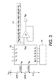
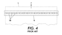
- an imaging apparatus comprising a video output line, at least a first plurality of photosensors adapted to output signals onto the video output line, and a voltage source.
- a DAC adjusts a voltage from the voltage source to associate a reference signal of a predetermined magnitude with the video output line.
Landscapes
- Engineering & Computer Science (AREA)
- Multimedia (AREA)
- Signal Processing (AREA)
- Facsimile Heads (AREA)
- Facsimile Image Signal Circuits (AREA)
- Solid State Image Pick-Up Elements (AREA)
Applications Claiming Priority (1)
| Application Number | Priority Date | Filing Date | Title |
|---|---|---|---|
| US11/158,571 US20060291008A1 (en) | 2005-06-22 | 2005-06-22 | System for adjusting a reference voltage in a photosensor chip |
Publications (1)
| Publication Number | Publication Date |
|---|---|
| EP1737218A2 true EP1737218A2 (de) | 2006-12-27 |
Family
ID=36579229
Family Applications (1)
| Application Number | Title | Priority Date | Filing Date |
|---|---|---|---|
| EP06114483A Withdrawn EP1737218A2 (de) | 2005-06-22 | 2006-05-24 | Sytème pour ajuster une tension de référence dans une puce photosensible |
Country Status (4)
| Country | Link |
|---|---|
| US (1) | US20060291008A1 (de) |
| EP (1) | EP1737218A2 (de) |
| JP (1) | JP2007006479A (de) |
| TW (1) | TW200711116A (de) |
Families Citing this family (4)
| Publication number | Priority date | Publication date | Assignee | Title |
|---|---|---|---|---|
| TW200919299A (en) * | 2007-08-01 | 2009-05-01 | Silverbrook Res Pty Ltd | Handheld scanner for coded surfaces |
| US7855748B2 (en) * | 2007-12-03 | 2010-12-21 | Altasens, Inc. | Reference voltage generation in imaging sensors |
| US8013282B2 (en) * | 2007-12-05 | 2011-09-06 | Xerox Corporation | System for programming a plurality of chips, such as photosensor chips or ink-jet chips, with operating parameters |
| US20120069229A1 (en) * | 2010-09-22 | 2012-03-22 | Xerox Corporation | Universal image sensor chip interface |
Family Cites Families (10)
| Publication number | Priority date | Publication date | Assignee | Title |
|---|---|---|---|---|
| US3924229A (en) * | 1969-01-10 | 1975-12-02 | Ibm | Bipolar digital to analog converter utilizing two reference voltages of the same polarity |
| US5654755A (en) * | 1996-01-05 | 1997-08-05 | Xerox Corporation | System for determining a video offset from dark photosensors in an image sensor array |
| EP0793380A2 (de) * | 1996-02-29 | 1997-09-03 | Kabushiki Kaisha Toshiba | Schaltung zur Rauschunterdrückung von Bildpunktsignalen und Bildaufnehmer damit |
| JP3075203B2 (ja) * | 1997-01-28 | 2000-08-14 | 日本電気株式会社 | 固体撮像素子 |
| SG70128A1 (en) * | 1997-10-06 | 2000-01-25 | Canon Kk | Method of driving image sensor |
| JP3226859B2 (ja) * | 1997-11-17 | 2001-11-05 | 日本電気株式会社 | 撮像装置 |
| US6657662B1 (en) * | 1999-09-03 | 2003-12-02 | Xerox Corporation | System for resetting the video offset from dark photosensors in an image sensor array |
| US6518910B2 (en) * | 2000-02-14 | 2003-02-11 | Canon Kabushiki Kaisha | Signal processing apparatus having an analog/digital conversion function |
| JP2003204486A (ja) * | 2002-01-09 | 2003-07-18 | Olympus Optical Co Ltd | 撮像装置 |
| US7038720B2 (en) * | 2002-10-16 | 2006-05-02 | Exar Corporation | Pixel-by-pixel digital control of gain and offset correction for video imaging |
-
2005
- 2005-06-22 US US11/158,571 patent/US20060291008A1/en not_active Abandoned
-
2006
- 2006-05-24 EP EP06114483A patent/EP1737218A2/de not_active Withdrawn
- 2006-06-14 TW TW095121234A patent/TW200711116A/zh unknown
- 2006-06-19 JP JP2006168429A patent/JP2007006479A/ja not_active Withdrawn
Also Published As
| Publication number | Publication date |
|---|---|
| JP2007006479A (ja) | 2007-01-11 |
| TW200711116A (en) | 2007-03-16 |
| US20060291008A1 (en) | 2006-12-28 |
Similar Documents
| Publication | Publication Date | Title |
|---|---|---|
| JP3287597B2 (ja) | 画像走査装置 | |
| US7746400B2 (en) | Method, apparatus, and system providing multi-column shared readout for imagers | |
| EP0773669B1 (de) | Schaltung, Bildelement, Vorrichtung und Verfahren zur Verminderung des Rauschens örtlich unveränderlicher Muster in Festkörperbildaufnahmevorrichtungen | |
| US5654755A (en) | System for determining a video offset from dark photosensors in an image sensor array | |
| US8212197B2 (en) | Image sensor with integration time compensation | |
| US20150098117A1 (en) | Imaging device, image reading apparatus, image forming apparatus, and image reading method | |
| CA2077378A1 (en) | Architecture for analog and digital image sensor arrays | |
| US6642496B1 (en) | Two dimensional optical shading gain compensation for imaging sensors | |
| JP2017216622A (ja) | 画像読取装置、及び画像形成装置、画像形成システム | |
| US9001246B2 (en) | Imaging apparatus, an imaging system, and a driving method of an imaging apparatus using correction data applied to pixels of same color | |
| US6445413B1 (en) | System for determining a video offset from dark photosensors in an image sensor array | |
| JP2007158663A (ja) | アナログ画像信号のオフセット調整方法 | |
| US7800787B2 (en) | Image reading apparatus | |
| US20020100863A1 (en) | Optical image scanner with color and intensity compensation during lamp warmup | |
| EP1737218A2 (de) | Sytème pour ajuster une tension de référence dans une puce photosensible | |
| US6853402B2 (en) | Combined multiplexing and offset correction for an image sensor array | |
| US7271380B2 (en) | Color input scanner calibration system | |
| US20060231734A1 (en) | Generation and storage of column offsets for a column parallel image sensor | |
| US7327500B2 (en) | Image inputting apparatus | |
| US5157500A (en) | Amplifier-return-driven CCD offset control for scanning arrays | |
| JP2856940B2 (ja) | 画像読取り装置 | |
| US6657662B1 (en) | System for resetting the video offset from dark photosensors in an image sensor array | |
| JP3792956B2 (ja) | 画像入力装置及びそれを用いた画像入力システム | |
| US7939788B2 (en) | Multi-chip photosensor with independently adjustable integration times for each chip | |
| JP2013038625A (ja) | 画像読取装置および画像形成装置 |
Legal Events
| Date | Code | Title | Description |
|---|---|---|---|
| PUAI | Public reference made under article 153(3) epc to a published international application that has entered the european phase |
Free format text: ORIGINAL CODE: 0009012 |
|
| AK | Designated contracting states |
Kind code of ref document: A2 Designated state(s): AT BE BG CH CY CZ DE DK EE ES FI FR GB GR HU IE IS IT LI LT LU LV MC NL PL PT RO SE SI SK TR |
|
| AX | Request for extension of the european patent |
Extension state: AL BA HR MK YU |
|
| STAA | Information on the status of an ep patent application or granted ep patent |
Free format text: STATUS: THE APPLICATION IS DEEMED TO BE WITHDRAWN |
|
| 18D | Application deemed to be withdrawn |
Effective date: 20090602 |