EP1740026A2 - Vorrichtung zum Entfernen von Fremdstoffen - Google Patents
Vorrichtung zum Entfernen von Fremdstoffen Download PDFInfo
- Publication number
- EP1740026A2 EP1740026A2 EP05255946A EP05255946A EP1740026A2 EP 1740026 A2 EP1740026 A2 EP 1740026A2 EP 05255946 A EP05255946 A EP 05255946A EP 05255946 A EP05255946 A EP 05255946A EP 1740026 A2 EP1740026 A2 EP 1740026A2
- Authority
- EP
- European Patent Office
- Prior art keywords
- foreign matter
- printed board
- board unit
- matter removing
- removing apparatus
- Prior art date
- Legal status (The legal status is an assumption and is not a legal conclusion. Google has not performed a legal analysis and makes no representation as to the accuracy of the status listed.)
- Withdrawn
Links
Images


Classifications
-
- B—PERFORMING OPERATIONS; TRANSPORTING
- B08—CLEANING
- B08B—CLEANING IN GENERAL; PREVENTION OF FOULING IN GENERAL
- B08B7/00—Cleaning by methods not provided for in a single other subclass or a single group in this subclass
- B08B7/02—Cleaning by methods not provided for in a single other subclass or a single group in this subclass by distortion, beating, or vibration of the surface to be cleaned
-
- H—ELECTRICITY
- H05—ELECTRIC TECHNIQUES NOT OTHERWISE PROVIDED FOR
- H05K—PRINTED CIRCUITS; CASINGS OR CONSTRUCTIONAL DETAILS OF ELECTRIC APPARATUS; MANUFACTURE OF ASSEMBLAGES OF ELECTRICAL COMPONENTS
- H05K3/00—Apparatus or processes for manufacturing printed circuits
- H05K3/22—Secondary treatment of printed circuits
- H05K3/26—Cleaning or polishing of the conductive pattern
-
- H—ELECTRICITY
- H05—ELECTRIC TECHNIQUES NOT OTHERWISE PROVIDED FOR
- H05K—PRINTED CIRCUITS; CASINGS OR CONSTRUCTIONAL DETAILS OF ELECTRIC APPARATUS; MANUFACTURE OF ASSEMBLAGES OF ELECTRICAL COMPONENTS
- H05K2203/00—Indexing scheme relating to apparatus or processes for manufacturing printed circuits covered by H05K3/00
- H05K2203/01—Tools for processing; Objects used during processing
- H05K2203/0147—Carriers and holders
- H05K2203/0165—Holder for holding a Printed Circuit Board [PCB] during processing, e.g. during screen printing
-
- H—ELECTRICITY
- H05—ELECTRIC TECHNIQUES NOT OTHERWISE PROVIDED FOR
- H05K—PRINTED CIRCUITS; CASINGS OR CONSTRUCTIONAL DETAILS OF ELECTRIC APPARATUS; MANUFACTURE OF ASSEMBLAGES OF ELECTRICAL COMPONENTS
- H05K2203/00—Indexing scheme relating to apparatus or processes for manufacturing printed circuits covered by H05K3/00
- H05K2203/02—Details related to mechanical or acoustic processing, e.g. drilling, punching, cutting, using ultrasound
- H05K2203/0292—Using vibration, e.g. during soldering or screen printing
-
- H—ELECTRICITY
- H05—ELECTRIC TECHNIQUES NOT OTHERWISE PROVIDED FOR
- H05K—PRINTED CIRCUITS; CASINGS OR CONSTRUCTIONAL DETAILS OF ELECTRIC APPARATUS; MANUFACTURE OF ASSEMBLAGES OF ELECTRICAL COMPONENTS
- H05K2203/00—Indexing scheme relating to apparatus or processes for manufacturing printed circuits covered by H05K3/00
- H05K2203/08—Treatments involving gases
- H05K2203/081—Blowing of gas, e.g. for cooling or for providing heat during solder reflowing
-
- H—ELECTRICITY
- H05—ELECTRIC TECHNIQUES NOT OTHERWISE PROVIDED FOR
- H05K—PRINTED CIRCUITS; CASINGS OR CONSTRUCTIONAL DETAILS OF ELECTRIC APPARATUS; MANUFACTURE OF ASSEMBLAGES OF ELECTRICAL COMPONENTS
- H05K2203/00—Indexing scheme relating to apparatus or processes for manufacturing printed circuits covered by H05K3/00
- H05K2203/08—Treatments involving gases
- H05K2203/082—Suction, e.g. for holding solder balls or components
-
- H—ELECTRICITY
- H10—SEMICONDUCTOR DEVICES; ELECTRIC SOLID-STATE DEVICES NOT OTHERWISE PROVIDED FOR
- H10W—GENERIC PACKAGES, INTERCONNECTIONS, CONNECTORS OR OTHER CONSTRUCTIONAL DETAILS OF DEVICES COVERED BY CLASS H10
- H10W90/00—Package configurations
- H10W90/701—Package configurations characterised by the relative positions of pads or connectors relative to package parts
- H10W90/721—Package configurations characterised by the relative positions of pads or connectors relative to package parts of bump connectors
- H10W90/724—Package configurations characterised by the relative positions of pads or connectors relative to package parts of bump connectors between a chip and a stacked insulating package substrate, interposer or RDL
Definitions
- the present invention relates to a foreign matter removing apparatus for removing foreign matter on a mounting surface of a printed board unit.
- a wafer chuck (see Japanese Patent Application Laid-open No.2000-195930 (pages 1 to 3, Fig. 1) for example) in which a chuck itself has a function for cleaning, using ultrasonic vibration, the chuck surface on which a wafer is placed in a semiconductor producing apparatus.
- Fig. 8 is a schematic diagram showing a foreign matter removing method of a conventional printed board unit
- Fig. 9 is an explanatory view of a problem in the foreign matter removing method shown in Fig. 8
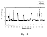
- Fig. 10 is a waveform diagram of shock wave in the foreign matter removing method of a conventional printed board unit.
- a striking which can apply shock wave of single waveform of about 5G acceleration two times per second is repeated thousands times on shock effective points 92 on a printed board 91 of a printed board unit 90 using a hammer 96, thereby removing foreign matter 95 entering a gap of mounted parts mounted on the printed board unit 90.
- BGA Bit Grid Array
- input/output terminal bumps 94 of the BGA 93 are disposed on the printed board unit at extremely narrow pitch and various patterns (normal/zigzag/random). Therefore, foreign matter 95 entering between the bumps 94 can not sufficiently be removed even if thousands repeated shocks by a hammer 96 and foreign matter remains in some cases. When the remaining foreign matter 95 is conductive foreign matter, short-circuit is generated between the terminals and thus, such printed board unit is discarded as failure part.
- a previously-proposed foreign matter removing method uses an air blow or vacuum instead of the foreign matter removing method using the shock wave.
- Fig. 11 is a schematic diagram of a foreign matter removing method utilizing air blow and vacuum
- Fig. 12 is a diagram showing a problem in the foreign matter removing method shown in Fig. 11.
- foreign matter 95 entering between the printed board 91 of the printed board unit 90 and the bumps 94 of the BGA 93 is removed using air flow caused by an air blow 97 and a vacuum 98.
- a foreign matter removing apparatus is an apparatus which removes foreign matter existing on a mounting surface of a printed board unit having parts mounted on the mounting surface, the foreign matter removing apparatus including:
- continuous shock wave is applied to the printed board unit in a state in which the printed board unit is held at its desired attitude. With this, it is possible to effectively remove foreign matter existing on the mounting surface of the printed board unit.
- the shock wave generator is an electromagnetic vibrator.
- the foreign matter removing apparatus of the invention has the above structure, it is possible to realize a foreign matter removing apparatus having excellent operability and maintenance performance.
- the holder holds the mounting surface downwardly.
- the foreign matter removing apparatus of the invention has the above structure, it is possible to effectively remove foreign matter entering into a connector mounted on the printed board unit.
- the apparatus further includes a blower which blows gas toward the printed board unit.
- the foreign matter removing apparatus of the invention has the above structure, it is possible to enhance the foreign matter removing effect of the foreign matter removing apparatus.
- the apparatus further includes a suction device which sucks gas from the printed board unit in addition to the blower.
- the foreign matter removing apparatus of the invention has the above structure, it is possible to enhance the foreign matter removing effect of the foreign matter removing apparatus.
- the apparatus further includes a foreign matter collector which collects foreign matter included in gas sucked by the suction device.
- the foreign matter removing apparatus of the invention has the above structure, it is possible to obtain useful information for enhancing quality of the printed board unit by analyzing the collected foreign matter.
- the apparatus further includes a sensor which measures intensity of shock received by the printed board unit from the continuous shock wave, and a monitoring unit which monitors a shock value measured by the sensor.
- the foreign matter removing apparatus of the invention has the above structure, since it is possible to easily monitor the intensity of shock received by the printed board unit, it is possible to prevent the printed board unit from being destroyed by excessive shock value.
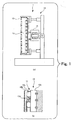
- Fig. 1 illustrates a schematic diagram (a) showing an embodiment of the foreign matter removing apparatus of the invention, and a partially enlarged diagram (b) thereof.
- the foreign matter removing apparatus 1 removes foreign matter 10d existing on a mounting surface 11 (see part (b) of Fig. 1) of a printed board unit 10.
- the foreign matter removing apparatus 1 includes a holder 14 which holds the printed board unit 10 in a desired attitude, an electromagnetic vibrator 15 which generates continuous shock wave having repeated waveform, and a transmitting plate 12 which transmits the continuous shock wave generated by the shock wave generator 15 to the printed board unit 10 held by the holder 14.
- the transmitting plate 12 of the embodiment corresponds to a transmitting member of the invention.
- the electromagnetic vibrator 15 of the embodiment corresponds to a shock wave generator of the invention.
- the shock wave generator is not limited to the electromagnetic vibrator, and any shock wave generator can be used only if it generates the continuous shock wave having repeated waveform, but it is preferable to use the electromagnetic vibrator in view of operability and maintenance performance.
- the printed board unit 10 is fixed in its inverted state by the holder 14 so that continuous shock wave generated by the electromagnetic vibrator 15 mounted on the printed board unit 10 on the opposite side from the mounting surface 11 is transmitted to the printed board unit 10 through the transmitting plate 12.
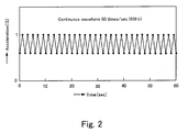
- Fig. 2 is a graph showing waveform of the continuous shock wave applied to the printed board unit.
- Fig. 2 shows a waveform of the continuous shock wave having repeated waveform of acceleration of about 0.7G and 60times/sec (60Hz).
- the product reliability enhancing effect obtained by applying the electromagnetic vibrator shock as compared with a previously-proposed hammer stroke is as follows: • shock (G) Previously-proposed technique: Ave 4.2, Max 6.7G Present invention: Ave 0.7, Max 1.0G Effect: Ave ⁇ 3.5G, Max ⁇ 5.7G That is, according to an embodiment of the invention, about 1/6 shock (G) of the previously-proposed technique is sufficient, and it is estimated that the product reliability is enhanced by six times.
- man-hour is reduced by 97% as compared with the previously-proposed technique, and it is estimated that the costs can largely be reduced.
- continuous shock wave having 30 times speed, 1/6 shock force and 1/3 stress as compared with the conventional hammer stroke is stably be supplied by the electromagnetic vibrator, and foreign matter such as dust existing on the printed board unit can effectively be removed.
- the foreign matter removing apparatus embodying the invention it is possible to reduce a danger that a printed board unit itself is destroyed by excessive shock exceeding the shock resistance that is a problem in a foreign matter removing method using the previously-proposed hammer stroke. Further, it is possible to overcome a problem that defectives are frequently produced in a screening stage during which failure of the printed board unit such as production failure and element failure of the printed board unit is removed.
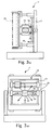
- Fig. 3 shows a shock position changing mechanism of the embodiment.
- the foreign matter removing apparatus 1' includes a shock position changing mechanism 19.
- the shock position changing mechanism 19 includes an X-direction slide bar 16 which supports the electromagnetic vibrator 15 such that the electromagnetic vibrator 15 can move in the X-direction, a slide bearing 18 which supports the X-direction slide bar 16, and a Y-direction slide bar 17 which supports the slide bearing 18 such that the slide bearing 18 can move in the Y-direction.
- the foreign matter removing apparatus 1' having the shock position changing mechanism 19 can freely change the shock position at which shock wave is supplied to the printed board unit 10 by the electromagnetic vibrator 15. Therefore, it is possible to efficiently remove foreign matter by moving the electromagnetic vibrator 15 to a shock position where foreign matter exists in the printed board unit 10 from which foreign matter is to be removed.
- Fig. 4 illustrates a schematic diagram (a) showing the second embodiment of the foreign matter removing apparatus of the invention, and an enlarged view (b) of collected foreign matter.
- the foreign matter removing apparatus 2 of the second embodiment includes a blowout fan unit 21 provided above the printed board unit 10 for blowing gas toward the printed board unit 10, and a vacuum unit 22 provided below the printed board unit 10 for sucking gas from the printed board unit 10. Foreign matter dropped by vibration is forcibly removed from the printed board unit 10 by the blowout fan unit 21 and the vacuum unit 22.
- the vacuum unit 22 is provided with a filter 23 for collecting foreign matter included in gas sucked by the vacuum unit 22, and the filter 23 can collect the dropped foreign matter 24 (see part (b) of Fig. 4). If the foreign matter 24 collected by the filter 23 is analyzed to grasp contents in the foreign matter 24, it is possible to obtain useful information for enhancing the quality of the printed board unit.
- the blowout fan unit 21 corresponds to a blower of an embodiment of the invention
- the vacuum unit 22 corresponds to a suction device of an embodiment of the invention
- the filter 23 corresponds to a foreign matter collector of an embodiment of the invention.
- Fig. 5 illustrates a schematic diagram (a) showing a foreign matter removing apparatus of the third embodiment, and a partial enlarged view (b) thereof.
- the holder 14 of the foreign matter removing apparatus 3 can hold the printed board unit 10 with any angle.
- continuous shock wave generated by the electromagnetic vibrator 15 is transmitted to the printed board unit 10 in a state in which the mounting surface 11 is held downwardly.
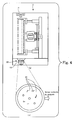
- Fig. 6 shows an outline of a foreign matter removing apparatus of a fourth embodiment
- Fig. 7 is a graph showing a shock value monitoring result by the foreign matter removing apparatus shown in Fig. 6.
- the foreign matter removing apparatus 4 includes G sensors 40 which measure the intensity of shock received by various portions of the printed board unit 10 by continuous shock wave, a monitoring unit 41 which monitors shock values measured by the G sensors 40, cables 42 which transmit measuring signals from the G sensors 40 to the monitoring unit 41, and a display unit 43 which displays a monitoring result on a screen.
- acceleration G intensity of shock
- the various portions CH1, CH2, CH3, Certainly, the various portions of the printed board unit 10 from the G sensors 40 and the monitoring unit 41 is displayed on the display unit 43. With this, it is possible to easily monitor the shock value received by the various portions of the printed board unit 10.
Landscapes
- Engineering & Computer Science (AREA)
- Manufacturing & Machinery (AREA)
- Microelectronics & Electronic Packaging (AREA)
- Cleaning In General (AREA)
Applications Claiming Priority (1)
| Application Number | Priority Date | Filing Date | Title |
|---|---|---|---|
| JP2005186145A JP2007000824A (ja) | 2005-06-27 | 2005-06-27 | 異物除去装置 |
Publications (2)
| Publication Number | Publication Date |
|---|---|
| EP1740026A2 true EP1740026A2 (de) | 2007-01-03 |
| EP1740026A3 EP1740026A3 (de) | 2007-08-01 |
Family
ID=37433816
Family Applications (1)
| Application Number | Title | Priority Date | Filing Date |
|---|---|---|---|
| EP05255946A Withdrawn EP1740026A3 (de) | 2005-06-27 | 2005-09-23 | Vorrichtung zum Entfernen von Fremdstoffen |
Country Status (3)
| Country | Link |
|---|---|
| US (1) | US20060288514A1 (de) |
| EP (1) | EP1740026A3 (de) |
| JP (1) | JP2007000824A (de) |
Cited By (3)
| Publication number | Priority date | Publication date | Assignee | Title |
|---|---|---|---|---|
| CN102764746A (zh) * | 2012-08-20 | 2012-11-07 | 戴若夫 | 一种电磁振动抖落滤尘芯积尘的振动器 |
| US9576929B1 (en) | 2015-12-30 | 2017-02-21 | Taiwan Semiconductor Manufacturing Company, Ltd. | Multi-strike process for bonding |
| CN110757997A (zh) * | 2018-10-27 | 2020-02-07 | 高宏福 | 一种封闭式板擦盒 |
Families Citing this family (6)
| Publication number | Priority date | Publication date | Assignee | Title |
|---|---|---|---|---|
| KR100933681B1 (ko) * | 2008-02-22 | 2009-12-23 | 성균관대학교산학협력단 | 무선 센서네트워크의 에너지와 거리 기반 클러스터링라우팅 방법 및 장치 |
| JP6107305B2 (ja) * | 2013-03-27 | 2017-04-05 | 大日本印刷株式会社 | ケースの洗浄方法およびケースの洗浄装置 |
| US10906244B2 (en) * | 2015-04-02 | 2021-02-02 | Xerox Corporation | Ultrasonic removal methods of three-dimensionally printed parts |
| CN108135093A (zh) * | 2017-12-28 | 2018-06-08 | 重庆市中光电显示技术有限公司 | 电路板清洁装置 |
| CN113770117B (zh) * | 2021-09-13 | 2022-11-08 | 常德富博智能科技有限公司 | 一种电源连板自动化测试装置 |
| CN117902280B (zh) * | 2024-01-19 | 2025-09-23 | 赣州市江元电子有限公司 | 一种自动送料的pcb板测量仪 |
Citations (2)
| Publication number | Priority date | Publication date | Assignee | Title |
|---|---|---|---|---|
| JPS5861543A (ja) | 1981-10-07 | 1983-04-12 | Nec Corp | ブラウン管の除塵方法 |
| JP2000195930A (ja) | 1998-12-28 | 2000-07-14 | Canon Inc | クリ―ニング機能を有するウエハチャックおよびウエハチャックのクリ―ニング方法 |
Family Cites Families (19)
| Publication number | Priority date | Publication date | Assignee | Title |
|---|---|---|---|---|
| US4501285A (en) * | 1982-04-05 | 1985-02-26 | Sonobond Ultrasonics, Inc. | Ultrasonic cleaning apparatus |
| JPH08155753A (ja) * | 1994-12-06 | 1996-06-18 | Sony Corp | プリント基板の塵埃除去装置 |
| US5766369A (en) * | 1995-10-05 | 1998-06-16 | Texas Instruments Incorporated | Method to reduce particulates in device manufacture |
| US5849135A (en) * | 1996-03-12 | 1998-12-15 | The Regents Of The University Of California | Particulate contamination removal from wafers using plasmas and mechanical agitation |
| JPH11191600A (ja) * | 1997-12-25 | 1999-07-13 | Nec Eng Ltd | Ccd用リードフレームのクリーニング方法および装置 |
| TW553780B (en) * | 1999-12-17 | 2003-09-21 | Sharp Kk | Ultrasonic processing device and electronic parts fabrication method using the same |
| US6543078B1 (en) * | 2000-07-24 | 2003-04-08 | Eastman Kodak Company | Apparatus and method for cleaning object having generally irregular surface features |
| US6766813B1 (en) * | 2000-08-01 | 2004-07-27 | Board Of Regents, The University Of Texas System | Apparatus and method for cleaning a wafer |
| US6723172B2 (en) * | 2000-08-18 | 2004-04-20 | Texas Instruments Incorporated | Method and system for processing semiconductor wafers |
| WO2003003428A2 (en) * | 2000-12-08 | 2003-01-09 | Deflex Llc | Apparatus, process and method for mounting and treating a substrate |
| JP2002217156A (ja) * | 2001-01-16 | 2002-08-02 | Hitachi Ltd | ドライ洗浄装置 |
| US20020129838A1 (en) * | 2001-03-15 | 2002-09-19 | Larry Myland | Substrate aspiration assembly |
| US6666927B2 (en) * | 2001-04-30 | 2003-12-23 | Intel Corporation | Vacuum debris removal system for an integrated circuit manufacturing device |
| JP3445982B2 (ja) * | 2001-07-19 | 2003-09-16 | 和喜 高山 | 衝撃波を用いた固体物表面の異物除去装置 |
| US6805137B2 (en) * | 2001-08-27 | 2004-10-19 | Applied Materials, Inc. | Method for removing contamination particles from substrates |
| US6779226B2 (en) * | 2001-08-27 | 2004-08-24 | Applied Materials, Inc. | Factory interface particle removal platform |
| JP2003200121A (ja) * | 2002-01-11 | 2003-07-15 | Ricoh Microelectronics Co Ltd | エアー洗浄装置 |
| US6676770B2 (en) * | 2002-03-19 | 2004-01-13 | Taiwan Semiconductor Manufacturing Co., Ltd. | Apparatus and method for removing particles from wafer pods |
| US7140066B1 (en) * | 2003-04-01 | 2006-11-28 | Itt Manufacturing Enterprises, Inc. | Apparatus and method for inspecting and cleaning semiconductor devices |
-
2005
- 2005-06-27 JP JP2005186145A patent/JP2007000824A/ja active Pending
- 2005-09-22 US US11/231,742 patent/US20060288514A1/en not_active Abandoned
- 2005-09-23 EP EP05255946A patent/EP1740026A3/de not_active Withdrawn
Patent Citations (2)
| Publication number | Priority date | Publication date | Assignee | Title |
|---|---|---|---|---|
| JPS5861543A (ja) | 1981-10-07 | 1983-04-12 | Nec Corp | ブラウン管の除塵方法 |
| JP2000195930A (ja) | 1998-12-28 | 2000-07-14 | Canon Inc | クリ―ニング機能を有するウエハチャックおよびウエハチャックのクリ―ニング方法 |
Cited By (6)
| Publication number | Priority date | Publication date | Assignee | Title |
|---|---|---|---|---|
| CN102764746A (zh) * | 2012-08-20 | 2012-11-07 | 戴若夫 | 一种电磁振动抖落滤尘芯积尘的振动器 |
| US9576929B1 (en) | 2015-12-30 | 2017-02-21 | Taiwan Semiconductor Manufacturing Company, Ltd. | Multi-strike process for bonding |
| DE102016101089A1 (de) * | 2015-12-30 | 2017-07-06 | Taiwan Semiconductor Manufacturing Company, Ltd. | Mehrfachaufprallprozess zum Bonden |
| US10068868B2 (en) | 2015-12-30 | 2018-09-04 | Taiwan Semiconductor Manufacturing Company, Ltd. | Multi-strike process for bonding packages and the packages thereof |
| DE102016101089B4 (de) | 2015-12-30 | 2020-06-18 | Taiwan Semiconductor Manufacturing Company, Ltd. | Mehrfachaufprallprozess zum Bonden |
| CN110757997A (zh) * | 2018-10-27 | 2020-02-07 | 高宏福 | 一种封闭式板擦盒 |
Also Published As
| Publication number | Publication date |
|---|---|
| JP2007000824A (ja) | 2007-01-11 |
| EP1740026A3 (de) | 2007-08-01 |
| US20060288514A1 (en) | 2006-12-28 |
Similar Documents
| Publication | Publication Date | Title |
|---|---|---|
| EP1740026A2 (de) | Vorrichtung zum Entfernen von Fremdstoffen | |
| KR101019080B1 (ko) | 미소 구조체의 검사 장치 및 미소 구조체의 검사 방법 | |
| CN101711189B (zh) | 用于振动器筛选装置的应力监视系统 | |
| JP2005067154A (ja) | 液滴視認方法、液滴吐出ヘッド検査装置および液滴吐出装置 | |
| JP2020524280A (ja) | 高分解能の表面粒子検出器 | |
| JPH01301145A (ja) | 実時間粒子降下モニター | |
| US20040065159A1 (en) | Impactor inlet | |
| JP2012083242A (ja) | 粒子計測方法及び粒子計測装置 | |
| JP2004012257A (ja) | ワークの外観検査装置および外観検査方法 | |
| CN113324580B (zh) | 基于感应电流和机器视觉的静电微滴喷射状态检测方法 | |
| JP2007188981A (ja) | 電子部品実装装置 | |
| JP3955423B2 (ja) | 粒子付着力測定装置及び付着力測定方法 | |
| CN210187918U (zh) | 用于印刷质量检测的除尘装置 | |
| CN101310876A (zh) | 一种感光器件的粉尘去除方法 | |
| CN105188337A (zh) | 颗粒噪声检测夹具、装置及方法 | |
| JP4512548B2 (ja) | 品質検査装置 | |
| US20090056761A1 (en) | Apparatus for maintaining a clean bonding enviroment | |
| CN113607274A (zh) | 一种噪音检测设备 | |
| CN114018927A (zh) | 一种物体碰撞恢复系数的测量方法 | |
| US3534589A (en) | Free particle and loose object detection system | |
| JP6761124B2 (ja) | 部品搭載装置、エアフィルタの清掃方法 | |
| JP2001074638A (ja) | 粒度分布測定装置 | |
| JP2010087842A (ja) | 圧電振動片用の折り取り冶具、折り取り装置、不良品折り取りシステム | |
| CN113102241A (zh) | 一种陶瓷生产原料过筛方法 | |
| CN217561434U (zh) | 一种烟尘烟气综合测试装置 |
Legal Events
| Date | Code | Title | Description |
|---|---|---|---|
| PUAI | Public reference made under article 153(3) epc to a published international application that has entered the european phase |
Free format text: ORIGINAL CODE: 0009012 |
|
| AK | Designated contracting states |
Kind code of ref document: A2 Designated state(s): AT BE BG CH CY CZ DE DK EE ES FI FR GB GR HU IE IS IT LI LT LU LV MC NL PL PT RO SE SI SK TR |
|
| AX | Request for extension of the european patent |
Extension state: AL BA HR MK YU |
|
| PUAL | Search report despatched |
Free format text: ORIGINAL CODE: 0009013 |
|
| AK | Designated contracting states |
Kind code of ref document: A3 Designated state(s): AT BE BG CH CY CZ DE DK EE ES FI FR GB GR HU IE IS IT LI LT LU LV MC NL PL PT RO SE SI SK TR |
|
| AX | Request for extension of the european patent |
Extension state: AL BA HR MK YU |
|
| 17P | Request for examination filed |
Effective date: 20080128 |
|
| AKX | Designation fees paid |
Designated state(s): DE FR GB |
|
| 17Q | First examination report despatched |
Effective date: 20110209 |
|
| STAA | Information on the status of an ep patent application or granted ep patent |
Free format text: STATUS: THE APPLICATION IS DEEMED TO BE WITHDRAWN |
|
| 18D | Application deemed to be withdrawn |
Effective date: 20110401 |