EP1741316B1 - Parallelplatten-elektronenvervielfacher mit ionenrückkopplungs-unterdrückung - Google Patents
Parallelplatten-elektronenvervielfacher mit ionenrückkopplungs-unterdrückung Download PDFInfo
- Publication number
- EP1741316B1 EP1741316B1 EP05712374.7A EP05712374A EP1741316B1 EP 1741316 B1 EP1741316 B1 EP 1741316B1 EP 05712374 A EP05712374 A EP 05712374A EP 1741316 B1 EP1741316 B1 EP 1741316B1
- Authority
- EP
- European Patent Office
- Prior art keywords
- electron
- electron multiplier
- plate
- channel
- interior surface
- Prior art date
- Legal status (The legal status is an assumption and is not a legal conclusion. Google has not performed a legal analysis and makes no representation as to the accuracy of the status listed.)
- Expired - Lifetime
Links
Images


Classifications
-
- H—ELECTRICITY
- H01—ELECTRIC ELEMENTS
- H01J—ELECTRIC DISCHARGE TUBES OR DISCHARGE LAMPS
- H01J43/00—Secondary-emission tubes; Electron-multiplier tubes
- H01J43/04—Electron multipliers
- H01J43/06—Electrode arrangements
- H01J43/18—Electrode arrangements using essentially more than one dynode
- H01J43/24—Dynodes having potential gradient along their surfaces
Definitions
- Electron multipliers are useful tools for various applications, including the detection of photons, electrons, ions and heavy particles. Such detectors are utilized in various spectroscopic techniques, including Auger electron spectroscopy (AES), x-ray photoelectron spectroscopy, ultraviolet photoelectron spectroscopy, and electron energy loss spectroscopy. Further, electron multipliers may be utilized for detection of secondary and back-scattered electrons in scanning electron microscopes, focused ion-beam tools, or e-beam lithography tools.
- AES Auger electron spectroscopy
- x-ray photoelectron spectroscopy x-ray photoelectron spectroscopy
- ultraviolet photoelectron spectroscopy ultraviolet photoelectron spectroscopy
- electron energy loss spectroscopy electron energy loss spectroscopy.
- electron multipliers may be utilized for detection of secondary and back-scattered electrons in scanning electron microscopes, focused ion-beam tools, or e-beam lithography tools.
- Typical electron multipliers are either channel type (e.g., multipliers that are tubular in nature) or flat plate type, including two flat plates that are usually parallel to each other.
- Channel electron multipliers can suppress ion feedback by shaping the channel (e.g., curved or spiraled) so that the travel distance of feedback ions is short.
- channel electron multipliers are not suitable for the detection of incoming charged or energetic neutral particles or photon beams with a cross sectional profile that is not round.
- Parallel plate electron multipliers can be shaped to accommodate beam profiles that are not round. However, due to the fact that they are usually constructed with flat parallel plates they are prone to ion feedback problems.
- US patent No. 5,117,149 discloses a number of embodiments of parallel plate electron multipliers, where the parallel surfaces defining the channel of non-planar cross-section, such as being C-shaped, arc-formed or having one or two right angles.
- the present invention relates to an electron multiplier according to the preamble of claim 1, which is distinguished from the prior art in that said first interior surface and said second interior surface define a channel of a cross-sectional shape that corresponds to either one period or two periods of a sinusoidal waveform.
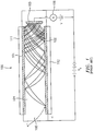
- FIG. 1 shows a conventional parallel plate electron multiplier 100.
- Electron multiplier 100 includes secondary emitting surfaces 101 and 102, deposited on glass plates 111 and 112, respectively, and separated by a channel 104.
- a voltage Vd is applied along the length of electron multiplier 100 so that electrons entering at an open end 105 are accelerated along the length of electron multiplier 100 away from open end 105.
- the secondary electrons are then accelerated along electron multiplier 100 and themselves may collide with one of secondary emitting surfaces 101 and 102.
- On each collision of an electron with sufficient kinetic energy with one of emitting surfaces 101 or 102 further electrons are emitted.
- an output pulse containing a very large number of electrons is emitted from electron multiplier 100.
- the output pulse is received by collector 103 located on the side of electron multiplier 100 opposite from open end 105. Typically, collector 103 is held at an elevated voltage from the voltage of that end of electron multiplier 100. The output pulse is detected by detection circuitry 106 coupled to collector 103.
- the gain of electron multiplier 100 depends on the voltage Vd applied across electron multiplier 100, the secondary emission properties of secondary emitting surfaces 101 and 102, and the physical dimensions of electron multiplier 100.
- Ion feedback causes a dispersion of the sensed signal as the ions travel backwards through channel 104 causing disbursed electron generation. This also provides excessive electron generation and a false reading at collector 103.
- Embodiments of the invention reduce ion feedback by utilizing a non-planar or curved channel between parallel plates.
- Figures 2A-2C depict an electron multiplier 200 in an embodiment of the invention.
- the electron multiplier 200 includes two plates 202 and 204 having parallel interior surfaces 206 and 208 defining a channel 210.
- the input end 212 of channel 210 has an increased dimension to facilitate electrons entering channel 210.
- Channel 210 is non-planar and is referred to as a single wave design as it corresponds to one period of a waveform (e.g., a sinusoid).
- Figures 3A-3C depict an electron multiplier 300 in an embodiment of the invention.
- the electron multiplier 300 includes two plates 302 and 304 having parallel interior surfaces 306 and 308 defining a channel 310.
- the input end 312 of channel 310 has an increased dimension to facilitate a beam entering channel 310.
- Channel 310 is non-planar and is referred to as a double wave design as it corresponds to two periods of a waveform (e.g., a sinusoid).
- Figures 4A-4C depict an electron multiplier 400 not part of the invention.
- the electron multiplier 400 includes two plates 402 and 404 having parallel interior surfaces 406 and 408 defining a channel 410.
- the input end 412 of channel 410 has an increased dimension to facilitate a beam entering channel 410.
- Channel 410 is non-planar and may be formed by thermally shaping glass plates.
- Figures 5A-5C depict an electron multiplier 500 not part of the invention.
- the electron multiplier 500 includes two plates 502 and 504 having parallel interior surfaces 506 and 508 defining a channel 510.
- the input end 512 of channel 510 has an increased dimension to facilitate a beam entering channel 510.
- Channel 510 is a non-planar, constant radius channel and plates 502 and 504 correspond to arcs of concentric cylinders.
- Figures 6A-6C depict an electron multiplier 600 not part of the invention.
- the electron multiplier 600 includes two plates 602 and 604 having parallel interior surfaces 606 and 608 defining a channel 610.
- the input end 612 of channel 610 has an increased dimension to facilitate a beam entering channel 610.
- Channel 610 is non-planar and plates 602 and 604 correspond to arcs of concentric cylinders.
- inventions of Figures 2-6 include a non-planar channel to reduce ion feedback.
- the non-planar channel limits the travel of ions in the channel thereby reducing the electron generation caused by ion feedback.
- Figure 7 depicts a cross sectional area of a multi-layer plate 700 utilized in embodiments of the invention.
- the first layer 701 is a support layer and allows the other layers to be positioned in a desirable orientation.
- the second layer 702 is a resistive layer that allows a voltage of a desired value to be placed across the multiplier to create an electric field that will accelerate generated electrons from the input or cathode end to the output or anode end.
- Layer 702 is resistive enough to support a biasing electric field without drawing excessive current and still be able to replenish electrons emitted from the emissive layer.
- the thickness and resistivity of the resistive layer should be uniform along the length of the channel to provide a constant electric field to accelerate the electrons toward the output end of the multiplier.
- the output end incorporates an anode that converts the electron pulse coming out of the channel into an electrical signal.
- the third layer 703 is an emissive layer.
- the multiplier makes use of the emissive layer to generate electron multiplication.
- the emissive surface will emit multiple electrons when struck by a charge or energetic neutral particle or photon of sufficient energy. The process is repeated down the length of the channel resulting the in multiplication process.
- the emissive layer has a secondary electron yield with an average greater than 1 to support the multiplication process.
- the layers depicted in Figure 7 can be formed of a single material such as a reduced lead oxide glass or a reduced bismuth oxide glass.
- an appropriate emissive material such as those listed below could be deposited onto a reduced lead oxide or reduced bismuth oxide glass.
- the layers can be formed separately.
- the emissive layer may be formed by a chemical vapor deposition (CVD) process.
- Materials that may be used for the emissive layer include but are not limited to diamond films, Al 2 O 3 , Si 3 N 4 , SiO 2 MgO, and BN.
- the semiconducting resistive layer may also be formed by a CVD process.
- the materials that may be used for this layer include but are not limited to Si, C, Ge, and Si 3 N 4 films that are doped to an appropriate resistivity.
- Substrate materials for the support layer include but are not limited to Al 2 O 3 , AlN, Si, SiO 2 glass, Si 3 N 4 , and SiC.
- Another example is a CVD silicon film doped to an appropriate resistivity deposited on a supporting substrate. Oxidation of the silicon forms the emissive layer.
- Embodiments of the invention overcome the difficulties with accommodating non-circular beam cross sections encountered with channel electron multipliers by employing parallel plate type of construction.
- the plates can be configured to form a detection region or channel of any desired geometry. This detection region can be used for detection of incoming charged or energetic neutral particle/photon beams with a variety of cross sectional areas.
- the channel can be used to accommodate beams having elliptical cross sections, rectangular cross sections, etc.
- Embodiments of the invention overcome the difficulties with ion feedback by utilizing a non-planar channel to limit the distance feedback ions can travel is formed.
- the channel can be formed so that the shape along the length of the multiplier is a curved path such as a wave shape or a section of a circle.
- Embodiments of the invention may be used to amplify electron, ion, photon, or energetic neutral signals. Embodiments of the invention may also be used as detectors in mass spectrometers for sample identification. Embodiments of the invention may also be used in surface analytical techniques such as Secondary Ion Mass Spectrometry (SIMS), Auger electron spectroscopy (AES), X-ray photoelectron spectroscopy, ultraviolet photoelectron spectroscopy, and electron energy loss spectroscopy. Embodiments of the invention may also be used for electron multiplication in a photon multiplier application and for detection of secondary and back-scattered electrons in electron microscopes, focused ion-beam tools and e-beam lithography.
- SIMS Secondary Ion Mass Spectrometry
- AES Auger electron spectroscopy
- X-ray photoelectron spectroscopy ultraviolet photoelectron spectroscopy
- Embodiments of the invention may also be used for electron multiplication in a
Landscapes
- Electron Tubes For Measurement (AREA)
Claims (11)
- Elektronenvervielfacher (200, 300), umfassend:eine erste Platte (202, 302), die eine erste Innenfläche (206, 306) aufweist, wobei die erste Innenfläche elektronenemittierend ist;eine zweite Platte (204, 304), die eine zweite Innenfläche (208, 308) aufweist, wobei die zweite Innenfläche elektronenemittierend ist;eine Spannungsquelle, die über die erste Platte und die zweite Platte angeschlossen ist;einen Kollektor, der in Antwort auf eine Elektronenvervielfachung durch die erste Platte und die zweite Platte ein Signal erzeugt;wobei die erste Innenfläche und die zweite Innenfläche parallel und nicht planar sind,dadurch gekennzeichnet, dassdie erste Innenfläche und die zweite Innenfläche einen Kanal (210, 310) mit einer Querschnittsform definieren, die entweder einer Periode oder zwei Perioden einer sinusförmigen Wellenform entspricht.
- Elektronenvervielfacher nach Anspruch 1, wobei:die erste Platte und die zweite Platte aus reduziertem Blei-Oxidglas oder reduziertem Bismut-Oxidglas hergestellt sind.
- Elektronenvervielfacher nach Anspruch 1, wobei:die erste Platte und die zweite Platte in mehreren Schichten ausgebildet sind.
- Elektronenvervielfacher nach Anspruch 3, wobei:eine der Schichten eine Trägerschicht ist.
- Elektronenvervielfacher nach Anspruch 4, wobei:die Trägerschicht aus Al2O3, AIN, Si, SiO2-Glas, Si3N4 oder SiC hergestellt ist.
- Elektronenvervielfacher nach Anspruch 3, wobei:eine der Schichten eine Widerstandsschicht ist.
- Elektronenvervielfacher nach Anspruch 6, wobei:die Widerstandsschicht aus Si, C, Ge oder Si3N4 hergestellt ist.
- Elektronenvervielfacher nach Anspruch 7, wobei:die Widerstandsschicht chemisch aufgedampft ist.
- Elektronenvervielfacher nach Anspruch 3, wobei:eine der Schichten eine elektronenemittierende Schicht ist.
- Elektronenvervielfacher nach Anspruch 9, wobei:die elektronenemittierende Schicht aus Diamantfilmen, Al2O3, Si3N4, SiO2, MgO oder BN hergestellt ist.
- Elektronenvervielfacher nach Anspruch 9, wobei:die elektronenemittierende Schicht chemisch aufgedampft ist.
Applications Claiming Priority (2)
| Application Number | Priority Date | Filing Date | Title |
|---|---|---|---|
| US10/770,309 US7042160B2 (en) | 2004-02-02 | 2004-02-02 | Parallel plate electron multiplier with ion feedback suppression |
| PCT/US2005/002912 WO2005074574A2 (en) | 2004-02-02 | 2005-01-31 | Parallel plate electron multiplier with ion feedback suppression |
Publications (3)
| Publication Number | Publication Date |
|---|---|
| EP1741316A2 EP1741316A2 (de) | 2007-01-10 |
| EP1741316A4 EP1741316A4 (de) | 2010-07-28 |
| EP1741316B1 true EP1741316B1 (de) | 2017-07-05 |
Family
ID=34808301
Family Applications (1)
| Application Number | Title | Priority Date | Filing Date |
|---|---|---|---|
| EP05712374.7A Expired - Lifetime EP1741316B1 (de) | 2004-02-02 | 2005-01-31 | Parallelplatten-elektronenvervielfacher mit ionenrückkopplungs-unterdrückung |
Country Status (5)
| Country | Link |
|---|---|
| US (1) | US7042160B2 (de) |
| EP (1) | EP1741316B1 (de) |
| JP (1) | JP2007520048A (de) |
| AU (1) | AU2005211418B2 (de) |
| WO (1) | WO2005074574A2 (de) |
Families Citing this family (6)
| Publication number | Priority date | Publication date | Assignee | Title |
|---|---|---|---|---|
| US20120286172A1 (en) * | 2011-05-12 | 2012-11-15 | Sefe, Inc. | Collection of Atmospheric Ions |
| JP6407767B2 (ja) | 2015-03-03 | 2018-10-17 | 浜松ホトニクス株式会社 | 電子増倍体の製造方法、光電子増倍管、及び光電子増倍器 |
| JP6474281B2 (ja) * | 2015-03-03 | 2019-02-27 | 浜松ホトニクス株式会社 | 電子増倍体、光電子増倍管、及び光電子増倍器 |
| JP6694033B2 (ja) * | 2018-09-19 | 2020-05-13 | 浜松ホトニクス株式会社 | 電子増倍体及び光電子増倍管 |
| RU2731363C1 (ru) * | 2019-12-26 | 2020-09-02 | Федеральное государственное автономное образовательное учреждение высшего образования "Национальный исследовательский университет "Московский институт электронной техники" | Вакуумный эмиссионный триод |
| JP7432459B2 (ja) * | 2020-07-15 | 2024-02-16 | 浜松ホトニクス株式会社 | チャネル型電子増倍体およびイオン検出器 |
Citations (1)
| Publication number | Priority date | Publication date | Assignee | Title |
|---|---|---|---|---|
| US3735184A (en) * | 1971-08-19 | 1973-05-22 | Matsushita Electric Industrial Co Ltd | Continuous dynode channel type secondary electron multiplier |
Family Cites Families (13)
| Publication number | Priority date | Publication date | Assignee | Title |
|---|---|---|---|---|
| US4095132A (en) * | 1964-09-11 | 1978-06-13 | Galileo Electro-Optics Corp. | Electron multiplier |
| JPS532533Y1 (de) * | 1970-11-16 | 1978-01-23 | ||
| CA958060A (en) * | 1971-05-03 | 1974-11-19 | Roger Pook | Image intensifiers |
| JPS55141455U (de) * | 1980-03-03 | 1980-10-09 | ||
| US4757229A (en) | 1986-11-19 | 1988-07-12 | K And M Electronics, Inc. | Channel electron multiplier |
| JPH01292737A (ja) * | 1988-05-19 | 1989-11-27 | Murata Mfg Co Ltd | 2次電子増倍装置 |
| US4978885A (en) * | 1989-03-02 | 1990-12-18 | Galileo Electro-Optics Corporation | Electron multipliers with reduced ion feedback |
| JPH0675388B2 (ja) * | 1989-03-16 | 1994-09-21 | 岐阜工業高等専門学校長 | 放射形二次電子増倍管 |
| US5374864A (en) | 1989-08-14 | 1994-12-20 | Detector Technology, Inc. | Electron multiplier with increased-area channel |
| US5117149A (en) | 1990-05-09 | 1992-05-26 | Galileo Electro-Optics Corporation | Parallel plate electron multiplier with negatively charged focussing strips and method of operation |
| US5440115A (en) * | 1994-04-05 | 1995-08-08 | Galileo Electro-Optics Corporation | Zener diode biased electron multiplier with stable gain characteristic |
| US6642637B1 (en) * | 2000-03-28 | 2003-11-04 | Applied Materials, Inc. | Parallel plate electron multiplier |
| JP3675326B2 (ja) * | 2000-10-06 | 2005-07-27 | キヤノン株式会社 | マルチチャネルプレートの製造方法 |
-
2004
- 2004-02-02 US US10/770,309 patent/US7042160B2/en not_active Expired - Lifetime
-
2005
- 2005-01-31 AU AU2005211418A patent/AU2005211418B2/en not_active Expired
- 2005-01-31 JP JP2006551526A patent/JP2007520048A/ja active Pending
- 2005-01-31 WO PCT/US2005/002912 patent/WO2005074574A2/en not_active Ceased
- 2005-01-31 EP EP05712374.7A patent/EP1741316B1/de not_active Expired - Lifetime
Patent Citations (1)
| Publication number | Priority date | Publication date | Assignee | Title |
|---|---|---|---|---|
| US3735184A (en) * | 1971-08-19 | 1973-05-22 | Matsushita Electric Industrial Co Ltd | Continuous dynode channel type secondary electron multiplier |
Also Published As
| Publication number | Publication date |
|---|---|
| EP1741316A4 (de) | 2010-07-28 |
| US7042160B2 (en) | 2006-05-09 |
| WO2005074574A2 (en) | 2005-08-18 |
| AU2005211418B2 (en) | 2010-06-17 |
| AU2005211418A1 (en) | 2005-08-18 |
| US20050168155A1 (en) | 2005-08-04 |
| JP2007520048A (ja) | 2007-07-19 |
| EP1741316A2 (de) | 2007-01-10 |
| WO2005074574A3 (en) | 2006-11-23 |
Similar Documents
| Publication | Publication Date | Title |
|---|---|---|
| US7141785B2 (en) | Ion detector | |
| Gys | Micro-channel plates and vacuum detectors | |
| US6617768B1 (en) | Multi dynode device and hybrid detector apparatus for mass spectrometry | |
| EP2297763B1 (de) | System und verfahren zur detektion geladener teilchen | |
| JP6329644B2 (ja) | 寿命が延長された直角飛行時間検出器 | |
| CN102782800B (zh) | 检测带电粒子的检测装置、检测带电粒子的方法以及质谱仪 | |
| US8686733B2 (en) | Ionization gauge having electron multiplier cold emission source | |
| KR20130114137A (ko) | 나노 다이아몬드층을 가지는 전자 증배기 장치 | |
| US6906318B2 (en) | Ion detector | |
| EP1741316B1 (de) | Parallelplatten-elektronenvervielfacher mit ionenrückkopplungs-unterdrückung | |
| JP6676383B2 (ja) | 飛行時間計測型質量分析装置 | |
| US7019446B2 (en) | Foil electron multiplier | |
| AU2007200596B2 (en) | Tandem Continuous Channel Electron Multiplier | |
| CA2457516C (en) | Ion detector | |
| US20230015584A1 (en) | Instruments including an electron multiplier | |
| US6642637B1 (en) | Parallel plate electron multiplier | |
| JP6690949B2 (ja) | 走査型電子顕微鏡 | |
| Furlong et al. | Secondary electron focusing in a metastable surface-detector | |
| JPH0439629B2 (de) | ||
| WO2006134344A2 (en) | Electron amplifier device |
Legal Events
| Date | Code | Title | Description |
|---|---|---|---|
| PUAI | Public reference made under article 153(3) epc to a published international application that has entered the european phase |
Free format text: ORIGINAL CODE: 0009012 |
|
| 17P | Request for examination filed |
Effective date: 20060706 |
|
| AK | Designated contracting states |
Kind code of ref document: A2 Designated state(s): AT BE BG CH CY CZ DE DK EE ES FI FR GB GR HU IE IS IT LI LT LU MC NL PL PT RO SE SI SK TR |
|
| AX | Request for extension of the european patent |
Extension state: AL BA HR LV MK YU |
|
| DAX | Request for extension of the european patent (deleted) | ||
| RBV | Designated contracting states (corrected) |
Designated state(s): DE FR GB |
|
| A4 | Supplementary search report drawn up and despatched |
Effective date: 20100630 |
|
| 17Q | First examination report despatched |
Effective date: 20101123 |
|
| RAP1 | Party data changed (applicant data changed or rights of an application transferred) |
Owner name: EXELIS, INC. |
|
| RAP1 | Party data changed (applicant data changed or rights of an application transferred) |
Owner name: EXELIS INC. |
|
| REG | Reference to a national code |
Ref country code: DE Ref legal event code: R079 Ref document number: 602005052248 Country of ref document: DE Free format text: PREVIOUS MAIN CLASS: H05B0037000000 Ipc: H01J0043240000 |
|
| GRAP | Despatch of communication of intention to grant a patent |
Free format text: ORIGINAL CODE: EPIDOSNIGR1 |
|
| RIC1 | Information provided on ipc code assigned before grant |
Ipc: H01J 43/24 20060101AFI20170120BHEP |
|
| INTG | Intention to grant announced |
Effective date: 20170209 |
|
| GRAS | Grant fee paid |
Free format text: ORIGINAL CODE: EPIDOSNIGR3 |
|
| GRAA | (expected) grant |
Free format text: ORIGINAL CODE: 0009210 |
|
| AK | Designated contracting states |
Kind code of ref document: B1 Designated state(s): DE FR GB |
|
| REG | Reference to a national code |
Ref country code: GB Ref legal event code: FG4D |
|
| REG | Reference to a national code |
Ref country code: DE Ref legal event code: R096 Ref document number: 602005052248 Country of ref document: DE |
|
| REG | Reference to a national code |
Ref country code: FR Ref legal event code: PLFP Year of fee payment: 14 |
|
| REG | Reference to a national code |
Ref country code: DE Ref legal event code: R097 Ref document number: 602005052248 Country of ref document: DE |
|
| PLBE | No opposition filed within time limit |
Free format text: ORIGINAL CODE: 0009261 |
|
| STAA | Information on the status of an ep patent application or granted ep patent |
Free format text: STATUS: NO OPPOSITION FILED WITHIN TIME LIMIT |
|
| 26N | No opposition filed |
Effective date: 20180406 |
|
| P01 | Opt-out of the competence of the unified patent court (upc) registered |
Effective date: 20230523 |
|
| PGFP | Annual fee paid to national office [announced via postgrant information from national office to epo] |
Ref country code: DE Payment date: 20240129 Year of fee payment: 20 Ref country code: GB Payment date: 20240129 Year of fee payment: 20 |
|
| PGFP | Annual fee paid to national office [announced via postgrant information from national office to epo] |
Ref country code: FR Payment date: 20240125 Year of fee payment: 20 |
|
| REG | Reference to a national code |
Ref country code: DE Ref legal event code: R071 Ref document number: 602005052248 Country of ref document: DE |
|
| REG | Reference to a national code |
Ref country code: GB Ref legal event code: PE20 Expiry date: 20250130 |
|
| PG25 | Lapsed in a contracting state [announced via postgrant information from national office to epo] |
Ref country code: GB Free format text: LAPSE BECAUSE OF EXPIRATION OF PROTECTION Effective date: 20250130 |