EP1741801A2 - Procédé de fabrication d'une couche de carbone amorphe - Google Patents
Procédé de fabrication d'une couche de carbone amorphe Download PDFInfo
- Publication number
- EP1741801A2 EP1741801A2 EP06011694A EP06011694A EP1741801A2 EP 1741801 A2 EP1741801 A2 EP 1741801A2 EP 06011694 A EP06011694 A EP 06011694A EP 06011694 A EP06011694 A EP 06011694A EP 1741801 A2 EP1741801 A2 EP 1741801A2
- Authority
- EP
- European Patent Office
- Prior art keywords
- film
- evaporation sources
- evaporation
- evaporation source
- magnetron sputtering
- Prior art date
- Legal status (The legal status is an assumption and is not a legal conclusion. Google has not performed a legal analysis and makes no representation as to the accuracy of the status listed.)
- Granted
Links
- 229910003481 amorphous carbon Inorganic materials 0.000 title claims abstract description 41
- 238000000034 method Methods 0.000 title claims abstract description 37
- 230000008020 evaporation Effects 0.000 claims abstract description 129
- 238000001704 evaporation Methods 0.000 claims abstract description 129
- 239000007789 gas Substances 0.000 claims abstract description 39
- 238000001755 magnetron sputter deposition Methods 0.000 claims abstract description 36
- OKTJSMMVPCPJKN-UHFFFAOYSA-N Carbon Chemical compound [C] OKTJSMMVPCPJKN-UHFFFAOYSA-N 0.000 claims abstract description 30
- 229910052799 carbon Inorganic materials 0.000 claims abstract description 30
- 239000007787 solid Substances 0.000 claims abstract description 21
- 238000004544 sputter deposition Methods 0.000 claims abstract description 16
- 239000012298 atmosphere Substances 0.000 claims abstract description 14
- 238000010891 electric arc Methods 0.000 claims abstract description 13
- 238000005477 sputtering target Methods 0.000 claims abstract description 8
- 239000013077 target material Substances 0.000 claims abstract description 6
- 239000011261 inert gas Substances 0.000 claims abstract description 5
- 238000000151 deposition Methods 0.000 description 59
- 230000008021 deposition Effects 0.000 description 45
- VNWKTOKETHGBQD-UHFFFAOYSA-N methane Chemical compound C VNWKTOKETHGBQD-UHFFFAOYSA-N 0.000 description 33
- 239000004215 Carbon black (E152) Substances 0.000 description 24
- 229930195733 hydrocarbon Natural products 0.000 description 24
- 150000002430 hydrocarbons Chemical class 0.000 description 24
- 239000011651 chromium Substances 0.000 description 13
- 230000000052 comparative effect Effects 0.000 description 12
- 229910052751 metal Inorganic materials 0.000 description 12
- 239000002184 metal Substances 0.000 description 12
- 239000000919 ceramic Substances 0.000 description 9
- 230000000694 effects Effects 0.000 description 9
- 238000005259 measurement Methods 0.000 description 7
- 229910052756 noble gas Inorganic materials 0.000 description 6
- 239000000758 substrate Substances 0.000 description 6
- XUIMIQQOPSSXEZ-UHFFFAOYSA-N Silicon Chemical compound [Si] XUIMIQQOPSSXEZ-UHFFFAOYSA-N 0.000 description 5
- 238000010586 diagram Methods 0.000 description 5
- 229910052710 silicon Inorganic materials 0.000 description 5
- 239000010703 silicon Substances 0.000 description 5
- XKRFYHLGVUSROY-UHFFFAOYSA-N Argon Chemical compound [Ar] XKRFYHLGVUSROY-UHFFFAOYSA-N 0.000 description 4
- VYZAMTAEIAYCRO-UHFFFAOYSA-N Chromium Chemical compound [Cr] VYZAMTAEIAYCRO-UHFFFAOYSA-N 0.000 description 4
- UHOVQNZJYSORNB-UHFFFAOYSA-N Benzene Chemical compound C1=CC=CC=C1 UHOVQNZJYSORNB-UHFFFAOYSA-N 0.000 description 3
- 230000005684 electric field Effects 0.000 description 3
- 230000002708 enhancing effect Effects 0.000 description 3
- 230000001133 acceleration Effects 0.000 description 2
- 229910052786 argon Inorganic materials 0.000 description 2
- 239000012300 argon atmosphere Substances 0.000 description 2
- 230000007423 decrease Effects 0.000 description 2
- 230000001965 increasing effect Effects 0.000 description 2
- 239000011159 matrix material Substances 0.000 description 2
- 238000009877 rendering Methods 0.000 description 2
- QYEXBYZXHDUPRC-UHFFFAOYSA-N B#[Ti]#B Chemical compound B#[Ti]#B QYEXBYZXHDUPRC-UHFFFAOYSA-N 0.000 description 1
- VGGSQFUCUMXWEO-UHFFFAOYSA-N Ethene Chemical compound C=C VGGSQFUCUMXWEO-UHFFFAOYSA-N 0.000 description 1
- 239000005977 Ethylene Substances 0.000 description 1
- CWYNVVGOOAEACU-UHFFFAOYSA-N Fe2+ Chemical compound [Fe+2] CWYNVVGOOAEACU-UHFFFAOYSA-N 0.000 description 1
- BGPVFRJUHWVFKM-UHFFFAOYSA-N N1=C2C=CC=CC2=[N+]([O-])C1(CC1)CCC21N=C1C=CC=CC1=[N+]2[O-] Chemical compound N1=C2C=CC=CC2=[N+]([O-])C1(CC1)CCC21N=C1C=CC=CC1=[N+]2[O-] BGPVFRJUHWVFKM-UHFFFAOYSA-N 0.000 description 1
- 229910033181 TiB2 Inorganic materials 0.000 description 1
- 230000015572 biosynthetic process Effects 0.000 description 1
- 239000000463 material Substances 0.000 description 1
- 150000002739 metals Chemical class 0.000 description 1
- 238000005268 plasma chemical vapour deposition Methods 0.000 description 1
- 230000027756 respiratory electron transport chain Effects 0.000 description 1
Images


Classifications
-
- C—CHEMISTRY; METALLURGY
- C23—COATING METALLIC MATERIAL; COATING MATERIAL WITH METALLIC MATERIAL; CHEMICAL SURFACE TREATMENT; DIFFUSION TREATMENT OF METALLIC MATERIAL; COATING BY VACUUM EVAPORATION, BY SPUTTERING, BY ION IMPLANTATION OR BY CHEMICAL VAPOUR DEPOSITION, IN GENERAL; INHIBITING CORROSION OF METALLIC MATERIAL OR INCRUSTATION IN GENERAL
- C23C—COATING METALLIC MATERIAL; COATING MATERIAL WITH METALLIC MATERIAL; SURFACE TREATMENT OF METALLIC MATERIAL BY DIFFUSION INTO THE SURFACE, BY CHEMICAL CONVERSION OR SUBSTITUTION; COATING BY VACUUM EVAPORATION, BY SPUTTERING, BY ION IMPLANTATION OR BY CHEMICAL VAPOUR DEPOSITION, IN GENERAL
- C23C14/00—Coating by vacuum evaporation, by sputtering or by ion implantation of the coating forming material
- C23C14/06—Coating by vacuum evaporation, by sputtering or by ion implantation of the coating forming material characterised by the coating material
- C23C14/0605—Carbon
-
- C—CHEMISTRY; METALLURGY
- C23—COATING METALLIC MATERIAL; COATING MATERIAL WITH METALLIC MATERIAL; CHEMICAL SURFACE TREATMENT; DIFFUSION TREATMENT OF METALLIC MATERIAL; COATING BY VACUUM EVAPORATION, BY SPUTTERING, BY ION IMPLANTATION OR BY CHEMICAL VAPOUR DEPOSITION, IN GENERAL; INHIBITING CORROSION OF METALLIC MATERIAL OR INCRUSTATION IN GENERAL
- C23C—COATING METALLIC MATERIAL; COATING MATERIAL WITH METALLIC MATERIAL; SURFACE TREATMENT OF METALLIC MATERIAL BY DIFFUSION INTO THE SURFACE, BY CHEMICAL CONVERSION OR SUBSTITUTION; COATING BY VACUUM EVAPORATION, BY SPUTTERING, BY ION IMPLANTATION OR BY CHEMICAL VAPOUR DEPOSITION, IN GENERAL
- C23C14/00—Coating by vacuum evaporation, by sputtering or by ion implantation of the coating forming material
- C23C14/22—Coating by vacuum evaporation, by sputtering or by ion implantation of the coating forming material characterised by the process of coating
- C23C14/34—Sputtering
- C23C14/35—Sputtering by application of a magnetic field, e.g. magnetron sputtering
-
- H—ELECTRICITY
- H01—ELECTRIC ELEMENTS
- H01J—ELECTRIC DISCHARGE TUBES OR DISCHARGE LAMPS
- H01J37/00—Discharge tubes with provision for introducing objects or material to be exposed to the discharge, e.g. for the purpose of examination or processing thereof
- H01J37/32—Gas-filled discharge tubes
- H01J37/32009—Arrangements for generation of plasma specially adapted for examination or treatment of objects, e.g. plasma sources
- H01J37/32055—Arc discharge
-
- H—ELECTRICITY
- H01—ELECTRIC ELEMENTS
- H01J—ELECTRIC DISCHARGE TUBES OR DISCHARGE LAMPS
- H01J37/00—Discharge tubes with provision for introducing objects or material to be exposed to the discharge, e.g. for the purpose of examination or processing thereof
- H01J37/32—Gas-filled discharge tubes
- H01J37/34—Gas-filled discharge tubes operating with cathodic sputtering
- H01J37/3402—Gas-filled discharge tubes operating with cathodic sputtering using supplementary magnetic fields
- H01J37/3405—Magnetron sputtering
Definitions
- This invention relates to a method for forming an amorphous carbon film, and in particular, to a method for forming an amorphous carbon film, used in sliding parts of machine components, and so forth.
- An amorphous carbon film (hereinafter referred to also as a DLC film) has high hardness and a smooth surface, and exhibits self-lubricity, so that it is used in machine components, and is lately put to use for dry-cutting of non-ferrous metal tools.
- a method for forming (film-deposition) the DLC film is broadly classified into a method for effecting the film-deposition from a gaseous material of a carbon-containing gas (methane, ethylene, benzene, and so forth) source by a plasma CVD process, and a method for effecting the film-deposition by a sputtering or arc process using a solid carbon supply source.
- a gaseous material of a carbon-containing gas methane, ethylene, benzene, and so forth
- the invention has been developed under the circumstances, and its object is to provide a method for forming an amorphous carbon film, capable of enhancing a deposition rate of the amorphous carbon film to thereby implementing deposition of the amorphous carbon film at a high speed.
- the inventors, et. al have conducted strenuous studies in order to attain the object as described, and as a result, have succeeded in achieving the present invention.
- One aspect of the invention is directed to a method for forming an amorphous carbon film, having the steps of: preparing at least two units of unbalancedmagnetron sputtering evaporation sources, or at least one unit each of the unbalanced magnetron sputtering evaporation source and a magnetic field applied arc-discharge evaporation source, and using a solid carbon as a sputtering target material of at least one unit of the unbalanced magnetron sputtering evaporation source among the evaporation sources to thereby turn an atmosphere into an atmosphere of a mixed gas of an inert gas for sputtering and a carbon-containing gas.
- respective magnetic fields of the evaporation sources are reversed in polarity from a magnetic field of the evaporation source adjacent to the respective evaporation sources, and a pulse potential at a frequency in a range of 50 to 400 kHz is imparted to the respective unbalanced magnetron sputtering evaporation sources.
- the method for forming an amorphous carbon film is further characterized in that the pulse potential is imparted at a duty cycle in a range of 50 to 80 %.
- the method for forming the amorphous carbon film makes it possible to enhance a deposition rate of the amorphous carbon film, and thereby forming the amorphous carbon film at a high speed.
- the inventors, et. al have conducted strenuous studies to attain the obj ect as described, and as a result, have succeeded in finding out that when depositing a DLC film by a sputtering method using a solid carbon for each of sputtering target materials of unbalanced magnetron sputtering evaporation sources, respective magnetic fields of the evaporation sources are reversed in polarity from a magnetic field of the evaporation source adjacent to the respective evaporation sources while hydrocarbon is introduced into a film-forming atmosphere, and a pulse potential at a frequency in a range of 50 to 400 kHz is applied to the respective evaporation sources so as to enable a film-deposition rate of the DLC film (an amorphous carbon film) to be enhanced, thereby depositing the DLC film at a high speed.
- the method for forming the amorphous carbon film is a method for forming an amorphous carbon film, comprising the steps of preparing at least two units of unbalanced magnetron sputtering evaporation sources, or at least one unit each of the unbalanced magnetron sputtering evaporation source, and a magnetic field applied arc-discharge evaporation source, and using a solid carbon as a sputtering target material of at least one unit of the unbalanced magnetron sputtering evaporation source among those evaporation sources to thereby turn an atmosphere into an atmosphere of a mixed gas of an inert gas for sputtering and a carbon-containing gas so as to form the amorphous carbon film, wherein respective magnetic fields of the those evaporation sources are reverse
- a magnetron sputtering method there is formed a space enclosed by lines of magnetic force in space in front of a target by the agency of magnets disposed on the back surface of the target. Electrons in plasma are trapped by the lines of magnetic force, and undergo cyclotron movement to thereby enhance probability of collision of the electrons with the inert gas, which is a sputter gas, that is, a noble gas (commonly, Ar), accelerating ionization of the noble gas element.
- a sputter gas that is, a noble gas (commonly, Ar), accelerating ionization of the noble gas element.
- a hydrocarbon gas for example, CH 4
- the hydrocarbon gas also collides with the electrons, whereupon parts of the hydrocarbon gas undergo ionization to be thereby deposited as the DLC film on a substrate.
- a sum of carbon sputtered from the target by the agency of the ionized element of the noble gas, and ionized parts of the hydrocarbon gas, as deposited, is recognized as the deposition rate of the DLC film.
- the deposition rate of the DLC film can be increased by applying a pulse potential. If the pulse potential is applied, this will cause a cyclically varying electric field to be produced in front of the target. The electrons trapped by the lines of the magnetic force in front of the target undergo vibration movement by the agency of the cyclically varying electric field while making the cyclotron movement.
- the noble gas + the hydrocarbon gas As the probability of the collision of the electrons with an atmospheric gas (the noble gas + the hydrocarbon gas) will further increase due to the vibration movement, it is deemed that ionization of the hydrocarbon gas is accelerated, and the ionization of the noble gas element is further accelerated to thereby increase sputtering from the carbon as the target, resulting in an increase in the deposition rate.
- the frequency of the pulse potential is preferably not lower than 100 kHz, and more preferably not lower than 200 kHz.
- the pulse potential to be applied may be either at a unipolar pulse undergoing variation between a minus potential and zero, or a bipolar pulse undergoing variation between a minus potential and a plus potential.
- gasses such as CH 4 , C 2 H 2 , C 2 H 4 , C 6 H 6 , and so forth.
- pressure at the time of the film-deposition a total pressure is preferably from 0.2 to 1 Pa, and a partial pressure of the hydrocarbon gas is preferably from 0.02 to 0.1 Pa.
- the electrons also undergo vibration movement by the agency of a pulsing electric field, but a ratio of electrons present in the vicinity of the substrate is high, so that an effect of an increase in the deposition rate, due to the ionization of the hydrocarbon gas, is higher in comparison with that in the case of a common magnetron layout. That is, in the case of using the unbalanced magnetron sputtering evaporation sources, the effect of an increase in the deposition rate, due to the ionization of the hydrocarbon gas, is higher than that in the case of using a magnetron sputtering evaporation source . Figs.
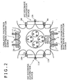
- FIG. 1 to 4 each show a film-forming apparatus using the unbalanced magnetron sputtering evaporation sources by way of example.
- two pieces of magnets that is, one magnet at the center and the other magnet in a ring-like shape, surrounding the one magnet, are disposed on the back surface of an evaporation source (sputtering target), and magnet parts 1, 3 (parts of the magnet in ring-like shape, on the outer sides thereof, as seen in section), disposed in the vicinity of respective ends of the evaporation source, each are greater in magnetic field strength than a magnet 2 (the magnet at the center) disposed at the center of the evaporation source.
- magnet parts 7, 9 parts of a magnet in ring-like shape, on the outer sides thereof, as seen in section
- magnet parts 4, 6 are greater in magnetic field strength than a magnet 5 (a magnet at the center).
- the film-forming apparatus comprising at least two units of the unbalancedmagnetron sputtering evaporation sources, or at least one unit each of the unbalanced magnetron sputtering evaporation source, and the magnetic field applied arc-discharge evaporation source, if the respective magnetic fields of the evaporation sources are reversed in polarity from the magnetic field of the evaporation source adjacent to the respective evaporation sources, lines of magnetic forces of the evaporation sources adjacent to each other come to be joined together as shown in Figs. 1 and 3 by way of example. In the case of an example shown in Fig.
- the magnet part (magnetic pole) 3 is the N-pole
- a magnet par 4A adjacent thereto is the S-pole
- the magnet parts 3, 4 are reversed in polarity from each other (being not the same in polarity, but opposite to each other in polarity)
- a magnet part 6A (the S-pole) and the magnet part 7 (the N-pole) are reversed in polarity from each other
- the magnet part 9 (the N-pole) and a magnet part 10A (the S-pole) are reversed in polarity from each other
- a magnet part 12A (the S-pole) are reversed in polarity from each other.
- the deposition rate of the DLC film is considerably enhanced. Accordingly, with the method for forming the amorphous carbon film, according to the invention, the deposition rate of the DLC film (the amorphous carbon film) can be sharply enhanced to thereby deposit the DLC film at a high speed.
- the pulse potential is preferably imparted at a duty cycle in a range of 50 to 80 % (a second invention) .
- the deposition rate of the DLC film can be enhanced at a high level with greater reliability to thereby deposit the DLC film at a high speed. This will be described in more details hereinafter.
- an increase in the deposition rate is recognized. More specifically, when a voltage is at 0V, or at a plus potential in the case of the bipolar pulse, no potential in effect occurs to the target, so that sputtering does not occur to the target.
- the duty cycle is preferably set to the range of 50 to 80 %, and if the duty cycle is set to the range of 50 to 80 %, the deposition rate of the DLC film can be enhanced at a high level with greater reliability.
- the duty cycle is more preferably set to a range of 60 to 75 %.
- the duty cycle (%) refers to a ratio of a load time period to one cycle of a recurring waveform.
- the duty cycle (%) upon imparting the pulse potential to the target is a ratio of a potential load time period (a time period during which a potential is kept occurring to the target) to one cycle of the recurring waveform of the pulse potential.
- the method for forming the amorphous carbon film there are prepared at least two units of the unbalanced magnetron sputtering evaporation sources, or at least one unit each of the unbalanced magnetron sputtering evaporation source, and the magnetic field applied arc-discharge evaporation source, and the solid carbon is used as the sputtering target material of at least one unit of the unbalanced magnetron sputtering evaporation source among those evaporation sources.
- a case (a) where the solid carbon is used for only one unit of the unbalanced magnetron sputtering evaporation source a case (b) where the solid carbon is used for several units of the unbalanced magnetron sputtering evaporation sources as well, other than the one unit of the unbalanced magnetron sputtering evaporation source; and a case (c) where the solid carbon is used for all units of the unbalanced magnetron sputtering evaporation sources; and any of those cases are to be construed within the scope of the method for forming the amorphous carbon film, according to the invention.
- metal, ceramics, and so forth may be used for the evaporation sources other than the evaporation source or sources, using the solid carbon.
- the DLC film (amorphous carbon film) composed of the amorphous carbon only can be obtained.
- the DLC film (amorphous carbon film) containing the metal evaporated from the evaporation sources can be obtained, and if ceramics is used for the evaporation sources other than the evaporation source or sources using the solid carbon, the DLC film (amorphous carbon film) containing the ceramics evaporated from the evaporation sources can be obtained.
- the magnetic field applied arc-discharge evaporation source refers to an arc-discharge evaporation source provided with magnets so as to enable magnetic fields to be applied thereto.
- the same is an evaporation source where the magnets are disposed to thereby produce the magnetic fields, such as, for example, an arc-discharge evaporation source shown in Fig. 1.
- the arc-discharge evaporation source refers to a type of evaporation source, causing evaporation to occur by arc discharge.
- a chromium metal target for forming an intermediate layer was used for one unit of the evaporation source of the unbalanced magnetron sputtering evaporation sources (2 units), and a solid carbon target was used for the other unit of the evaporation source. Further, a layout was adopted such that respective magnetic fields of the evaporation sources are reversed in polarity from a magnetic field of the evaporation source adjacent to the respective evaporation sources, thereby causing lines of magnetic forces of the evaporation sources adjacent to each other to be joined together, as shown in Fig. 1.
- a silicon wafer used for measurement of a deposition rate.
- An input power for sputtering was set to 2 kW at a pulse peak.
- a chromium metal film (100 nm) as the intermediate layer was formed on the silicon wafer.
- An atmosphere at the time of forming the intermediate layer composed of Cr was an argon atmosphere at a pressure of 0.6 Pa.
- a total pressure at 0.6 Pa was kept constant while a hydrocarbon gas was introduced at 10 % of a volumetric ratio (a ratio of the volume of the hydrocarbon gas to the volume of Ar together with the hydrocarbon gas), namely, at a partial pressure of 0.06 Pa, thereby having formed the DLC film.
- a voltage applied to a substrate upon film-deposition was set to 50 V at the time of forming the intermediate layer composed of Cr, and to 100 V at the time of forming the DLC film.
- the silicon wafer with both the intermediate layer composed of Cr and the DLC film deposited thereon was cut, and the cross-section thereof was observed by an SEM in a magnification range of 10,000 to 20,000 x, to thereby find a film thickness of the DLC film. Then, the deposition rate (film-forming speed) of the DLC film was found by computation on the basis of a film thickness of the DLC film, and film-deposition time.
- the respective magnetic fields of the evaporation sources are rendered the same in polarity as the magnetic field of the evaporation source adjacent to the respective evaporation sources, thereby causing the lines of the magnetic forces of the evaporation sources adjacent to each other not to be joined together, as shown in Fig. 2.
- Deposition of an intermediate layer composed of Cr and a DLC film was carried out in the same manner as in the case of item (A) as above, except for those points described, and subsequently, in the same manner as in the case of item (A) as above, measurement of a film thickness of the DLC film was executed by observation of the cross section thereof while a deposition rate of the DLC film was computed.
- a duty cycle upon impartation of a pulse potential at the time of deposition of a DLC film was varied.
- the deposition of an intermediate layer composed of Cr and a DLC film was carried out in the same manner as in the case of the example 1 (A) as above, except for a point described, and subsequently, in the same manner as in the case of the example 1 (A) as above, measurement of a film thickness of the DLC film was executed by observation of the cross section thereof while a deposition rate of the DLC film was computed.
- a film-forming apparatus use was made of the same film-forming apparatus as was used in the case of the example 1 (A). That is, a layout was adopted such that lines of magnetic forces of evaporation sources adjacent to each other are caused to be joined together, as shown in Fig. 1.
- a chromium metal target for forming an intermediate layer was used for the evaporation source a
- a solid carbon target was used for the evaporation source b
- any among a variety of metals or ceramics is attached to the evaporation source c.
- a layout was adopted such that lines of magnetic forces of evaporation sources adjacent to each other are caused to be joined together, as shown in Fig. 3.
- a silicon wafer For a matrix, use was made of a silicon wafer. A chromium metal film (100 nm) as the intermediate layer was formed on the silicon wafer as with the case of the example 1 (A). An atmosphere at the time of forming the intermediate layer composed of Cr metal was an argon atmosphere at a pressure of 0.6 Pa, as with the case of the example 1 (A).
- the evaporation source b (the solid carbon target), and the evaporation source c (metal or ceramics evaporation source) are caused to undergo concurrent discharge, thereby having deposited the DLC film containing the metal or the ceramics.
- an input power to the evaporation source b (the solid carbon target) was set to 2 kW at a pulse peak, as with the case of the example 1 (A)
- an input power to the evaporation source c (metal or ceramics evaporation source) was set to 0.1 kW.
- An atmosphere at the time of film-deposition was at a total pressure of 0. 6 Pa, kept constant, as with the case of the example 1 (A), and a hydrocarbon gas was introduced at 10 % of a volumetric ratio, namely, at a partial pressure of 0.06 Pa, thereby having deposited the DLC film.
- the method for forming the amorphous carbon film is capable of enhancing the film-deposition rate of the amorphous carbon film, and forming the amorphous carbon film at a high speed, so that the invention is useful as it can be suitably used for the method for forming the amorphous carbon film to thereby attain enhancement in productivity of the amorphous carbon film.
Landscapes
- Chemical & Material Sciences (AREA)
- Engineering & Computer Science (AREA)
- Organic Chemistry (AREA)
- Materials Engineering (AREA)
- Mechanical Engineering (AREA)
- Metallurgy (AREA)
- Chemical Kinetics & Catalysis (AREA)
- Physics & Mathematics (AREA)
- Plasma & Fusion (AREA)
- Analytical Chemistry (AREA)
- Physical Vapour Deposition (AREA)
- Manufacturing Of Magnetic Record Carriers (AREA)
- Carbon And Carbon Compounds (AREA)
- Glass Compositions (AREA)
Applications Claiming Priority (1)
| Application Number | Priority Date | Filing Date | Title |
|---|---|---|---|
| JP2005195303A JP4607687B2 (ja) | 2005-07-04 | 2005-07-04 | 非晶質炭素膜の成膜方法 |
Publications (3)
| Publication Number | Publication Date |
|---|---|
| EP1741801A2 true EP1741801A2 (fr) | 2007-01-10 |
| EP1741801A3 EP1741801A3 (fr) | 2007-09-05 |
| EP1741801B1 EP1741801B1 (fr) | 2009-08-12 |
Family
ID=36716897
Family Applications (1)
| Application Number | Title | Priority Date | Filing Date |
|---|---|---|---|
| EP06011694A Not-in-force EP1741801B1 (fr) | 2005-07-04 | 2006-06-06 | Procédé de fabrication d'une couche de carbone amorphe |
Country Status (6)
| Country | Link |
|---|---|
| US (1) | US20070000770A1 (fr) |
| EP (1) | EP1741801B1 (fr) |
| JP (1) | JP4607687B2 (fr) |
| KR (1) | KR100776888B1 (fr) |
| AT (1) | ATE439456T1 (fr) |
| DE (1) | DE602006008389D1 (fr) |
Cited By (5)
| Publication number | Priority date | Publication date | Assignee | Title |
|---|---|---|---|---|
| GB2437730A (en) * | 2006-05-02 | 2007-11-07 | Univ Sheffield Hallam | HIPIMS with low magnetic field strength |
| WO2009052874A1 (fr) * | 2007-10-26 | 2009-04-30 | Hauzer Techno Coating Bv | Alimentation électrique de pulvérisation à double magnétron et appareil de pulvérisation à magnétron |
| CN102719799A (zh) * | 2012-06-08 | 2012-10-10 | 深圳市华星光电技术有限公司 | 旋转磁控溅射靶及相应的磁控溅射装置 |
| CN104328380A (zh) * | 2014-07-31 | 2015-02-04 | 宁夏天马滚动体制造有限公司 | 轴承滚柱非平衡磁控溅射离子镀装置及方法 |
| EP2587519A3 (fr) * | 2011-10-28 | 2015-10-21 | Kabushiki Kaisha Kobe Seiko Sho | Appareil de formation de film et procédé de formation de film |
Families Citing this family (10)
| Publication number | Priority date | Publication date | Assignee | Title |
|---|---|---|---|---|
| KR100796766B1 (ko) * | 2006-05-29 | 2008-01-22 | (주)레드로버 | 프로젝션용 스테레오 광학엔진 구조 |
| KR100893675B1 (ko) * | 2007-05-11 | 2009-04-17 | 주식회사 테스 | 비정질 탄소막 형성 방법 및 이를 이용한 반도체 소자의제조 방법 |
| WO2009079358A1 (fr) * | 2007-12-14 | 2009-06-25 | The Regents Of The University Of California | Pulvérisation haute puissance par magnétron déclenchée par impulsions à très faible pression |
| CN103298967B (zh) | 2010-12-08 | 2016-07-06 | 盖伦国际公司 | 硬且低摩擦的氮化物涂层 |
| EP2680238A4 (fr) * | 2011-02-22 | 2015-04-08 | Glory Kogyo Kk | Dispositif de traitement d'argent liquide, système de traitement d'argent liquide, cassette de transport d'argent liquide, dispositif de traitement de billets et procédé de traitement de billets |
| US10304665B2 (en) | 2011-09-07 | 2019-05-28 | Nano-Product Engineering, LLC | Reactors for plasma-assisted processes and associated methods |
| US9761424B1 (en) | 2011-09-07 | 2017-09-12 | Nano-Product Engineering, LLC | Filtered cathodic arc method, apparatus and applications thereof |
| US11834204B1 (en) | 2018-04-05 | 2023-12-05 | Nano-Product Engineering, LLC | Sources for plasma assisted electric propulsion |
| EP3938556A1 (fr) * | 2019-03-15 | 2022-01-19 | Nanofilm Technologies International Limited | Procédés de revêtement améliorés |
| CN114717512B (zh) * | 2022-04-21 | 2023-02-28 | 中国科学院兰州化学物理研究所 | 一种自适应长效润滑性能金/碳复合薄膜的制备方法 |
Family Cites Families (13)
| Publication number | Priority date | Publication date | Assignee | Title |
|---|---|---|---|---|
| GB9006073D0 (en) * | 1990-03-17 | 1990-05-16 | D G Teer Coating Services Limi | Magnetron sputter ion plating |
| JPH06145975A (ja) * | 1992-03-20 | 1994-05-27 | Komag Inc | 炭素フィルムをスパタリングする方法及びその製造物 |
| DE19651615C1 (de) * | 1996-12-12 | 1997-07-10 | Fraunhofer Ges Forschung | Verfahren zum Aufbringen von Kohlenstoffschichten durch reaktives Magnetron-Sputtern |
| DE19740793C2 (de) * | 1997-09-17 | 2003-03-20 | Bosch Gmbh Robert | Verfahren zur Beschichtung von Oberflächen mittels einer Anlage mit Sputterelektroden und Verwendung des Verfahrens |
| US6726993B2 (en) * | 1997-12-02 | 2004-04-27 | Teer Coatings Limited | Carbon coatings, method and apparatus for applying them, and articles bearing such coatings |
| JP3172139B2 (ja) * | 1998-08-04 | 2001-06-04 | 富士写真フイルム株式会社 | サーマルヘッド |
| US6338777B1 (en) * | 1998-10-23 | 2002-01-15 | International Business Machines Corporation | Method and apparatus for sputtering thin films |
| JP2001150351A (ja) * | 1999-11-19 | 2001-06-05 | Noritake Diamond Ind Co Ltd | ドレッシング用電着砥石 |
| JP4615697B2 (ja) * | 2000-11-07 | 2011-01-19 | ティーア、コーティングズ、リミテッド | 炭素含有被覆を施した物品 |
| JP2002367138A (ja) * | 2001-06-07 | 2002-12-20 | Fujitsu Ltd | 磁気情報記録媒体 |
| JP4360082B2 (ja) * | 2001-12-17 | 2009-11-11 | 住友電気工業株式会社 | 非晶質炭素被膜の製造方法及び非晶質炭素被覆摺動部品 |
| JP2004285440A (ja) * | 2003-03-24 | 2004-10-14 | Daiwa Kogyo Kk | Hcd・ubmsハイブリッドpvd法およびその装置 |
| JP2005138208A (ja) * | 2003-11-05 | 2005-06-02 | Sumitomo Electric Hardmetal Corp | 表面被覆切削工具とその作製方法 |
-
2005
- 2005-07-04 JP JP2005195303A patent/JP4607687B2/ja not_active Expired - Fee Related
-
2006
- 2006-05-31 US US11/421,240 patent/US20070000770A1/en not_active Abandoned
- 2006-06-06 EP EP06011694A patent/EP1741801B1/fr not_active Not-in-force
- 2006-06-06 DE DE602006008389T patent/DE602006008389D1/de active Active
- 2006-06-06 AT AT06011694T patent/ATE439456T1/de not_active IP Right Cessation
- 2006-07-03 KR KR1020060062101A patent/KR100776888B1/ko not_active Expired - Fee Related
Cited By (5)
| Publication number | Priority date | Publication date | Assignee | Title |
|---|---|---|---|---|
| GB2437730A (en) * | 2006-05-02 | 2007-11-07 | Univ Sheffield Hallam | HIPIMS with low magnetic field strength |
| WO2009052874A1 (fr) * | 2007-10-26 | 2009-04-30 | Hauzer Techno Coating Bv | Alimentation électrique de pulvérisation à double magnétron et appareil de pulvérisation à magnétron |
| EP2587519A3 (fr) * | 2011-10-28 | 2015-10-21 | Kabushiki Kaisha Kobe Seiko Sho | Appareil de formation de film et procédé de formation de film |
| CN102719799A (zh) * | 2012-06-08 | 2012-10-10 | 深圳市华星光电技术有限公司 | 旋转磁控溅射靶及相应的磁控溅射装置 |
| CN104328380A (zh) * | 2014-07-31 | 2015-02-04 | 宁夏天马滚动体制造有限公司 | 轴承滚柱非平衡磁控溅射离子镀装置及方法 |
Also Published As
| Publication number | Publication date |
|---|---|
| JP2007009310A (ja) | 2007-01-18 |
| US20070000770A1 (en) | 2007-01-04 |
| DE602006008389D1 (de) | 2009-09-24 |
| ATE439456T1 (de) | 2009-08-15 |
| EP1741801A3 (fr) | 2007-09-05 |
| EP1741801B1 (fr) | 2009-08-12 |
| JP4607687B2 (ja) | 2011-01-05 |
| KR100776888B1 (ko) | 2007-11-19 |
| KR20070004449A (ko) | 2007-01-09 |
Similar Documents
| Publication | Publication Date | Title |
|---|---|---|
| EP1741801B1 (fr) | Procédé de fabrication d'une couche de carbone amorphe | |
| US7081186B2 (en) | Combined coating process comprising magnetic field-assisted, high power, pulsed cathode sputtering and an unbalanced magnetron | |
| US20090200158A1 (en) | High power impulse magnetron sputtering vapour deposition | |
| EP2383366B1 (fr) | Procédé de production d'une membrane en carbone de type diamant | |
| CN109267007A (zh) | 用于在工件上沉积无氢四面体非晶碳层的装置和方法 | |
| Ganesan et al. | Pulse length selection in bipolar HiPIMS for high deposition rate of smooth, hard amorphous carbon films | |
| US20050136656A1 (en) | Process for depositing composite coating on a surface | |
| JP4449187B2 (ja) | 薄膜形成方法 | |
| CN104674168A (zh) | 一种聚合物高分子材料等离子体表面改性工艺 | |
| CN109504947B (zh) | 一种CrN涂层、制备方法及应用 | |
| KR101231668B1 (ko) | 스퍼터링 장치 및 스퍼터링 방법 | |
| KR101108894B1 (ko) | 스퍼터링용 타겟 및 이 타겟을 이용한 스퍼터링 방법 | |
| JP2007035623A (ja) | プラズマ活性を向上させる装置 | |
| CN1623008A (zh) | 氮化钛膜的形成方法 | |
| JPH01129958A (ja) | 高密着窒化チタン膜形成方法 | |
| US8134287B1 (en) | Low voltage closed drift anode layer ion source | |
| CN101838789B (zh) | 减小由物理气相沉积生成的镀膜中的压力的方法 | |
| KR101231669B1 (ko) | 스퍼터링 장치 및 스퍼터링 방법 | |
| JPS6217175A (ja) | スパツタリング装置 | |
| JP2004353023A (ja) | アーク放電方式のイオンプレーティング装置 | |
| JP3056827B2 (ja) | ダイヤモンド様炭素保護膜を有する物品とその製造方法 | |
| Hara et al. | Compound-layer-free nitriding of ferrous metals using electron-beam-excited nitrogen plasma | |
| CN113366601A (zh) | 等离子体源的用于执行等离子体处理的磁体装置 | |
| JPS63458A (ja) | 真空ア−ク蒸着装置 | |
| JP6569900B2 (ja) | スパッタリング装置および成膜方法 |
Legal Events
| Date | Code | Title | Description |
|---|---|---|---|
| PUAI | Public reference made under article 153(3) epc to a published international application that has entered the european phase |
Free format text: ORIGINAL CODE: 0009012 |
|
| AK | Designated contracting states |
Kind code of ref document: A2 Designated state(s): AT BE BG CH CY CZ DE DK EE ES FI FR GB GR HU IE IS IT LI LT LU LV MC NL PL PT RO SE SI SK TR |
|
| AX | Request for extension of the european patent |
Extension state: AL BA HR MK YU |
|
| PUAL | Search report despatched |
Free format text: ORIGINAL CODE: 0009013 |
|
| AK | Designated contracting states |
Kind code of ref document: A3 Designated state(s): AT BE BG CH CY CZ DE DK EE ES FI FR GB GR HU IE IS IT LI LT LU LV MC NL PL PT RO SE SI SK TR |
|
| AX | Request for extension of the european patent |
Extension state: AL BA HR MK YU |
|
| RIC1 | Information provided on ipc code assigned before grant |
Ipc: C23C 14/35 20060101ALI20070731BHEP Ipc: C23C 14/06 20060101AFI20060804BHEP |
|
| 17P | Request for examination filed |
Effective date: 20071213 |
|
| AKX | Designation fees paid |
Designated state(s): AT DE FR NL SE |
|
| GRAP | Despatch of communication of intention to grant a patent |
Free format text: ORIGINAL CODE: EPIDOSNIGR1 |
|
| GRAC | Information related to communication of intention to grant a patent modified |
Free format text: ORIGINAL CODE: EPIDOSCIGR1 |
|
| GRAS | Grant fee paid |
Free format text: ORIGINAL CODE: EPIDOSNIGR3 |
|
| GRAA | (expected) grant |
Free format text: ORIGINAL CODE: 0009210 |
|
| AK | Designated contracting states |
Kind code of ref document: B1 Designated state(s): AT DE FR NL SE |
|
| REF | Corresponds to: |
Ref document number: 602006008389 Country of ref document: DE Date of ref document: 20090924 Kind code of ref document: P |
|
| REG | Reference to a national code |
Ref country code: SE Ref legal event code: TRGR |
|
| PG25 | Lapsed in a contracting state [announced via postgrant information from national office to epo] |
Ref country code: AT Free format text: LAPSE BECAUSE OF FAILURE TO SUBMIT A TRANSLATION OF THE DESCRIPTION OR TO PAY THE FEE WITHIN THE PRESCRIBED TIME-LIMIT Effective date: 20090812 |
|
| NLV1 | Nl: lapsed or annulled due to failure to fulfill the requirements of art. 29p and 29m of the patents act | ||
| PG25 | Lapsed in a contracting state [announced via postgrant information from national office to epo] |
Ref country code: NL Free format text: LAPSE BECAUSE OF FAILURE TO SUBMIT A TRANSLATION OF THE DESCRIPTION OR TO PAY THE FEE WITHIN THE PRESCRIBED TIME-LIMIT Effective date: 20090812 |
|
| PLBE | No opposition filed within time limit |
Free format text: ORIGINAL CODE: 0009261 |
|
| STAA | Information on the status of an ep patent application or granted ep patent |
Free format text: STATUS: NO OPPOSITION FILED WITHIN TIME LIMIT |
|
| 26N | No opposition filed |
Effective date: 20100517 |
|
| REG | Reference to a national code |
Ref country code: FR Ref legal event code: PLFP Year of fee payment: 11 |
|
| REG | Reference to a national code |
Ref country code: FR Ref legal event code: PLFP Year of fee payment: 12 |
|
| REG | Reference to a national code |
Ref country code: FR Ref legal event code: PLFP Year of fee payment: 13 |
|
| PGFP | Annual fee paid to national office [announced via postgrant information from national office to epo] |
Ref country code: DE Payment date: 20210511 Year of fee payment: 16 Ref country code: FR Payment date: 20210513 Year of fee payment: 16 |
|
| PGFP | Annual fee paid to national office [announced via postgrant information from national office to epo] |
Ref country code: SE Payment date: 20210610 Year of fee payment: 16 |
|
| REG | Reference to a national code |
Ref country code: DE Ref legal event code: R119 Ref document number: 602006008389 Country of ref document: DE |
|
| REG | Reference to a national code |
Ref country code: SE Ref legal event code: EUG |
|
| PG25 | Lapsed in a contracting state [announced via postgrant information from national office to epo] |
Ref country code: SE Free format text: LAPSE BECAUSE OF NON-PAYMENT OF DUE FEES Effective date: 20220607 Ref country code: FR Free format text: LAPSE BECAUSE OF NON-PAYMENT OF DUE FEES Effective date: 20220630 |
|
| PG25 | Lapsed in a contracting state [announced via postgrant information from national office to epo] |
Ref country code: DE Free format text: LAPSE BECAUSE OF NON-PAYMENT OF DUE FEES Effective date: 20230103 |