EP1742092A1 - Messmethode zur Messung der Verstimmung eines optischen Signals, Messgerät, optischer Transmitter und optisches Modul - Google Patents
Messmethode zur Messung der Verstimmung eines optischen Signals, Messgerät, optischer Transmitter und optisches Modul Download PDFInfo
- Publication number
- EP1742092A1 EP1742092A1 EP05291486A EP05291486A EP1742092A1 EP 1742092 A1 EP1742092 A1 EP 1742092A1 EP 05291486 A EP05291486 A EP 05291486A EP 05291486 A EP05291486 A EP 05291486A EP 1742092 A1 EP1742092 A1 EP 1742092A1
- Authority
- EP
- European Patent Office
- Prior art keywords
- mach
- signal
- output
- measuring
- zehnder
- Prior art date
- Legal status (The legal status is an assumption and is not a legal conclusion. Google has not performed a legal analysis and makes no representation as to the accuracy of the status listed.)
- Withdrawn
Links
Images


Classifications
-
- G—PHYSICS
- G01—MEASURING; TESTING
- G01J—MEASUREMENT OF INTENSITY, VELOCITY, SPECTRAL CONTENT, POLARISATION, PHASE OR PULSE CHARACTERISTICS OF INFRARED, VISIBLE OR ULTRAVIOLET LIGHT; COLORIMETRY; RADIATION PYROMETRY
- G01J9/00—Measuring optical phase difference; Determining degree of coherence; Measuring optical wavelength
- G01J9/02—Measuring optical phase difference; Determining degree of coherence; Measuring optical wavelength by interferometric methods
- G01J9/0246—Measuring optical wavelength
-
- G—PHYSICS
- G02—OPTICS
- G02B—OPTICAL ELEMENTS, SYSTEMS OR APPARATUS
- G02B6/00—Light guides; Structural details of arrangements comprising light guides and other optical elements, e.g. couplings
- G02B6/24—Coupling light guides
- G02B6/26—Optical coupling means
- G02B6/28—Optical coupling means having data bus means, i.e. plural waveguides interconnected and providing an inherently bidirectional system by mixing and splitting signals
- G02B6/293—Optical coupling means having data bus means, i.e. plural waveguides interconnected and providing an inherently bidirectional system by mixing and splitting signals with wavelength selective means
- G02B6/29346—Optical coupling means having data bus means, i.e. plural waveguides interconnected and providing an inherently bidirectional system by mixing and splitting signals with wavelength selective means operating by wave or beam interference
- G02B6/2935—Mach-Zehnder configuration, i.e. comprising separate splitting and combining means
- G02B6/29352—Mach-Zehnder configuration, i.e. comprising separate splitting and combining means in a light guide
-
- G—PHYSICS
- G02—OPTICS
- G02B—OPTICAL ELEMENTS, SYSTEMS OR APPARATUS
- G02B6/00—Light guides; Structural details of arrangements comprising light guides and other optical elements, e.g. couplings
- G02B6/24—Coupling light guides
- G02B6/26—Optical coupling means
- G02B6/28—Optical coupling means having data bus means, i.e. plural waveguides interconnected and providing an inherently bidirectional system by mixing and splitting signals
- G02B6/293—Optical coupling means having data bus means, i.e. plural waveguides interconnected and providing an inherently bidirectional system by mixing and splitting signals with wavelength selective means
- G02B6/29379—Optical coupling means having data bus means, i.e. plural waveguides interconnected and providing an inherently bidirectional system by mixing and splitting signals with wavelength selective means characterised by the function or use of the complete device
- G02B6/2938—Optical coupling means having data bus means, i.e. plural waveguides interconnected and providing an inherently bidirectional system by mixing and splitting signals with wavelength selective means characterised by the function or use of the complete device for multiplexing or demultiplexing, i.e. combining or separating wavelengths, e.g. 1xN, NxM
- G02B6/29382—Optical coupling means having data bus means, i.e. plural waveguides interconnected and providing an inherently bidirectional system by mixing and splitting signals with wavelength selective means characterised by the function or use of the complete device for multiplexing or demultiplexing, i.e. combining or separating wavelengths, e.g. 1xN, NxM including at least adding or dropping a signal, i.e. passing the majority of signals
- G02B6/29383—Adding and dropping
-
- G—PHYSICS
- G02—OPTICS
- G02B—OPTICAL ELEMENTS, SYSTEMS OR APPARATUS
- G02B6/00—Light guides; Structural details of arrangements comprising light guides and other optical elements, e.g. couplings
- G02B6/24—Coupling light guides
- G02B6/26—Optical coupling means
- G02B6/28—Optical coupling means having data bus means, i.e. plural waveguides interconnected and providing an inherently bidirectional system by mixing and splitting signals
- G02B6/293—Optical coupling means having data bus means, i.e. plural waveguides interconnected and providing an inherently bidirectional system by mixing and splitting signals with wavelength selective means
- G02B6/29379—Optical coupling means having data bus means, i.e. plural waveguides interconnected and providing an inherently bidirectional system by mixing and splitting signals with wavelength selective means characterised by the function or use of the complete device
- G02B6/29395—Optical coupling means having data bus means, i.e. plural waveguides interconnected and providing an inherently bidirectional system by mixing and splitting signals with wavelength selective means characterised by the function or use of the complete device configurable, e.g. tunable or reconfigurable
Definitions
- the invention relates to a measuring method for measuring the detuning of an optical signal, according to the preamble of claim 1, a measuring device according to the preamble of claim 2, and an optical transmitter according to the preamble of claim 3.
- Transmitter lasers in such an area are subject to ageing and temperature induced wavelength drifts.
- the invention starts from dealing with a network with a wavelength allocation scheme with 20 nm wide wavebands. On either side of such a waveband there are edges between pass band and stop band that take up some 3 - 3.5 nm. This means that for the operation remains only some 13 - 14 nm.
- Typical DFB laser drifts over the temperature range -40° ... + 85°C lie in the range of 12.5 nm. This means that there is practically no tolerance left for manufacturing or ageing.
- the problem now is to provide a basis for tuning the optical source such that the optical signal remains within the pass band.
- the invention uses the sinusoidal characteristic of a Mach-Zehnder device and especially uses the quasi-linear part of one falling or raising slope thereof.
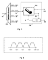
- Figure 1 shows a CWDM demultiplexer DM and an optical module OM.
- the demultiplexer DM has one input connected to a distribution line DL and four outputs connected each with a subscriber line, one of which is denoted SL.
- the optical module OM includes an optical transceiver TRX and a control unit CU.
- the transceiver TRX is connected with the subscriber line SL, with a signal input and output line SIO, with a measuring output line MO and with a tuning input line TI.
- the control unit CU is connected with the measuring output line MO, the tuning input line TI, and a signaling line Sig.
- the invention expects, that the whole optical module OM is integrated into what is shown here as transceiver TRX.
- Figure 2 shows the pass bands of the CWDM demultiplexer DM of figure 1.
- this is the characteristic of a filter bank with four pass band filters identical in shape, but dislocated one against the other by the width of one single pass band filter.
- Each path band filter clearly shows a rising edge and a falling edge as described in the introductory part.
- this CWDM demultiplexer DM works with passive elements, in the upstream direction it works as a multiplexer.
- Figure 3 shows a part of an optical module according to the invention, including a measuring device MD according to the invention.
- the continuous optical line shown at the top of this figure connects the subscriber line SL with the signal input and output line SIO'.
- the signal input and output line is denominated SIO' instead of SIO and is shown as being an optical line like the subscriber line SL. That is because figure 3 (and figure 4) shows only what is necessary to understand the invention. Of course those parts not shown here in detail nevertheless are necessary.
- An optical coupler OC drops a signal either from the far end to a far-end input f (solid line) of the measuring device MD or from the near end to a near-end input n (dotted) of the measuring device MD or both.
- the measuring device MD includes a Mach-Zehnder device MZ, two photo diodes, PD1 and PD2, with a following amplifier each, a subtracter Sub, an adder Add, a switch SW, and a divider Div.
- the Mach-Zehnder device MZ is built in the usual manner with two optical couplers and a delay element in either of the connections between the two couplers.
- the delay element should bring an optical delta of 60 micrometer.
- an input signal swept over the considered wavelength range will result in an output signal at either output with a sinusoidal behavior and a period of 40 nm at 1540 nm.
- the period of 40 nm will become clearer in connection with the description of figure 5.
- the necessary values will become obvious to a person skilled in the art.
- the two photo diodes, PD1 and PD2 in connection with the two amplifiers perform the conversion into electrical signals.
- the subtractor Sub builds the difference between the amplitudes at the two outputs of the Mach-Zehnder device MZ.
- the switch SW gives the possibility to invert the signal output by the subtractor Sub. With this one can achieve that the output characteristic of the subtractor over the wavelength has the same slope in each wavelength band. Without this one would have falling slopes in every other band and raising slopes in between. This will become clearer when reading the description concerning figure 5b. Of course such inversion or not inversion can be made fixed instead of switchable, when considering only one wavelength band. And it is possible to do it elsewhere.
- the adder Add adds the amplitudes at the two outputs of the Mach-Zehnder device MZ, thus building a value indicating the total power Int of the measured signal. If necessary, such value can be output for other purposes.
- the divider Div divides the output value of the switch SW by the output value of the adder Add and thus normalizes the result. This value is given to the measuring output line MO.
- figure 1 shows what may be done with the value output on the measuring output line MO. This value is input into the control unit CU.
- the control unit CU When one wants to tune the laser in the far end, one has to measure via the far-end input f as shown in figure 3. Of course it is to be ensured, that during such measuring there will be no input signal at the near-end input n. Then the control unit CU has to prepare a signal to be given to the signaling line Sig. Such signal may be a protocol sequence to be sent to the far end via the normal data channel led through the signal input and output line SIO.
- Figure 4 shows a situation slightly different from that of figure 3.
- the subscriber line SL, and the signal input and output line SIO' are fiber pairs with one fiber for each direction.
- an optical coupler OCn in the outgoing fiber or an optical coupler OCf in the coming fiber or both are fiber pairs with one fiber for each direction.
- an optical coupler OCn in the outgoing fiber or an optical coupler OCf in the coming fiber or both are fiber pairs with one fiber for each direction.
- an optical coupler OCn in the outgoing fiber or an optical coupler OCf in the coming fiber or both.
- the signal at the output in the direction away from the laser The rest is the same as in figure 3.
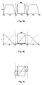
- Figure 5a shows schematically the characteristic of a filter with three adjacent pass bands in a more realistic presentation than in figure 2.
- the wavelength band considered here is depicted as a rectangle and denominated as PB.
- PB flat-top region
- Figure 5b shows the situation at the output of the Mach-Zehnder device MZ under the assumption that there is no band filtering in front of the Mach-Zehnder device MZ.
- the characteristics at both outputs show sine waves each, solid and dotted line, respectively. (This has nothing to do with the solid and dotted lines in figures 3 and 4). Both sine waves have a phase difference between each other of 180°. There is another phase difference of 180° between the considered band and the two adjacent ones. That is why the switch SW as described in connection with figure 3 is foreseen. Thus for further processing the signals output from the Mach-Zehnder device MZ one can always establish the same situation.
- figure 5c shows the difference between the two characteristics shown in figure 5b, multiplied by the characteristic shown in figure 5a. That is the situation at the output of the subtractor Sub as described in connection with figure 3, when measuring an optical signal coming from the far end. Without band limiting the input signal, especially when measuring the near-end signal, there are no such deep slopes as within the ellipses in figure 5c.
Landscapes
- Physics & Mathematics (AREA)
- General Physics & Mathematics (AREA)
- Optics & Photonics (AREA)
- Spectroscopy & Molecular Physics (AREA)
- Optical Communication System (AREA)
Priority Applications (1)
| Application Number | Priority Date | Filing Date | Title |
|---|---|---|---|
| EP05291486A EP1742092A1 (de) | 2005-07-04 | 2005-07-04 | Messmethode zur Messung der Verstimmung eines optischen Signals, Messgerät, optischer Transmitter und optisches Modul |
Applications Claiming Priority (1)
| Application Number | Priority Date | Filing Date | Title |
|---|---|---|---|
| EP05291486A EP1742092A1 (de) | 2005-07-04 | 2005-07-04 | Messmethode zur Messung der Verstimmung eines optischen Signals, Messgerät, optischer Transmitter und optisches Modul |
Publications (1)
| Publication Number | Publication Date |
|---|---|
| EP1742092A1 true EP1742092A1 (de) | 2007-01-10 |
Family
ID=35355369
Family Applications (1)
| Application Number | Title | Priority Date | Filing Date |
|---|---|---|---|
| EP05291486A Withdrawn EP1742092A1 (de) | 2005-07-04 | 2005-07-04 | Messmethode zur Messung der Verstimmung eines optischen Signals, Messgerät, optischer Transmitter und optisches Modul |
Country Status (1)
| Country | Link |
|---|---|
| EP (1) | EP1742092A1 (de) |
Citations (5)
| Publication number | Priority date | Publication date | Assignee | Title |
|---|---|---|---|---|
| EP0481242A2 (de) * | 1990-09-20 | 1992-04-22 | Fujitsu Limited | Vorrichtung zur Steuerung und Messung der optischen Frequenztastung von Laserlicht |
| EP0505048A2 (de) * | 1991-03-21 | 1992-09-23 | Nortel Networks Corporation | Optischer FSK-Modulator |
| JPH0595153A (ja) * | 1991-10-01 | 1993-04-16 | Nippon Telegr & Teleph Corp <Ntt> | 光fsk周波数偏移安定化回路 |
| EP0607029A2 (de) * | 1993-01-14 | 1994-07-20 | Nippon Telegraph And Telephone Corporation | Optisches bidirektionales Kommunikationssystem mit Wellenlängenmultiplex |
| US20020149780A1 (en) * | 2001-03-07 | 2002-10-17 | Paul Trinh | Integrated-optic channel monitoring |
-
2005
- 2005-07-04 EP EP05291486A patent/EP1742092A1/de not_active Withdrawn
Patent Citations (5)
| Publication number | Priority date | Publication date | Assignee | Title |
|---|---|---|---|---|
| EP0481242A2 (de) * | 1990-09-20 | 1992-04-22 | Fujitsu Limited | Vorrichtung zur Steuerung und Messung der optischen Frequenztastung von Laserlicht |
| EP0505048A2 (de) * | 1991-03-21 | 1992-09-23 | Nortel Networks Corporation | Optischer FSK-Modulator |
| JPH0595153A (ja) * | 1991-10-01 | 1993-04-16 | Nippon Telegr & Teleph Corp <Ntt> | 光fsk周波数偏移安定化回路 |
| EP0607029A2 (de) * | 1993-01-14 | 1994-07-20 | Nippon Telegraph And Telephone Corporation | Optisches bidirektionales Kommunikationssystem mit Wellenlängenmultiplex |
| US20020149780A1 (en) * | 2001-03-07 | 2002-10-17 | Paul Trinh | Integrated-optic channel monitoring |
Non-Patent Citations (1)
| Title |
|---|
| PATENT ABSTRACTS OF JAPAN vol. 017, no. 444 (E - 1415) 16 August 1993 (1993-08-16) * |
Similar Documents
| Publication | Publication Date | Title |
|---|---|---|
| EP0985289B1 (de) | Optisches multiplexing und demultiplexing | |
| US5410624A (en) | Filter for a wavelength division multiplex system | |
| US6373604B1 (en) | Optical MUX/DEMUX | |
| US7773839B2 (en) | Optical dispersion compensation | |
| Giles et al. | The wavelength add/drop multiplexer for lightwave communication networks | |
| KR20010041551A (ko) | 분산 보상용 광 소자 | |
| CN102272643A (zh) | 光合分波电路以及使用光合分波电路的光模块和光通信系统 | |
| TWI234668B (en) | Fiber Bragg grating sensing system of light intensity and wave-divided multiplex | |
| JP2020122936A (ja) | 波長可変フィルタ及び光学システム | |
| WO2000049690A1 (en) | Compact wavelength-independent wavelength-locker for absolute wavelength stability of a laser diode | |
| US8761597B2 (en) | Monitoring node and reflector node of an optical communication network, optical communication network, and method for operating an optical communication network | |
| CA2394655A1 (en) | Method and device for locking the wavelength of an optical signal | |
| US7474854B2 (en) | Optical transmission system | |
| EP1742092A1 (de) | Messmethode zur Messung der Verstimmung eines optischen Signals, Messgerät, optischer Transmitter und optisches Modul | |
| US20020130256A1 (en) | Spectrum, time and protocol domain optical performance monitor | |
| JP2005091165A (ja) | Fbgセンシングシステム | |
| US6546160B1 (en) | Transceiver for wavelength multiplexing processes | |
| EP1748580A1 (de) | Verfahren zur Überprüfung der Integrität einer optischen Zugangsleitung | |
| CN101180815B (zh) | 用于在光波长转换器中减小串扰的系统 | |
| US20020141010A1 (en) | Coupled data and wavelength reference for optical performance monitoring in fiber optic systems | |
| US20090316286A1 (en) | Aligned Narrowband Optical Filters having Flat Passbands and Comprising Offset Cascaded Broadband Optical Filters | |
| CN104104430B (zh) | 频率校准方法及装置 | |
| JP2600507B2 (ja) | 光合分波器 | |
| EP0880249A2 (de) | System zur Unterdrückung von Vierwellenmischlicht (FWM) | |
| EP4589349A1 (de) | Optische integrierte schaltung und optischer empfänger |
Legal Events
| Date | Code | Title | Description |
|---|---|---|---|
| PUAI | Public reference made under article 153(3) epc to a published international application that has entered the european phase |
Free format text: ORIGINAL CODE: 0009012 |
|
| AK | Designated contracting states |
Kind code of ref document: A1 Designated state(s): AT BE BG CH CY CZ DE DK EE ES FI FR GB GR HU IE IS IT LI LT LU LV MC NL PL PT RO SE SI SK TR |
|
| AX | Request for extension of the european patent |
Extension state: AL BA HR MK YU |
|
| RAP1 | Party data changed (applicant data changed or rights of an application transferred) |
Owner name: ALCATEL LUCENT |
|
| 17P | Request for examination filed |
Effective date: 20070710 |
|
| 17Q | First examination report despatched |
Effective date: 20070809 |
|
| AKX | Designation fees paid |
Designated state(s): AT BE BG CH CY CZ DE DK EE ES FI FR GB GR HU IE IS IT LI LT LU LV MC NL PL PT RO SE SI SK TR |
|
| STAA | Information on the status of an ep patent application or granted ep patent |
Free format text: STATUS: THE APPLICATION IS DEEMED TO BE WITHDRAWN |
|
| 18D | Application deemed to be withdrawn |
Effective date: 20071220 |