EP1742245A2 - Schwarze Grünfolienoberschicht, Plasma-Anzeigetafel und Verfahren zur deren Herstellung - Google Patents
Schwarze Grünfolienoberschicht, Plasma-Anzeigetafel und Verfahren zur deren Herstellung Download PDFInfo
- Publication number
- EP1742245A2 EP1742245A2 EP06291128A EP06291128A EP1742245A2 EP 1742245 A2 EP1742245 A2 EP 1742245A2 EP 06291128 A EP06291128 A EP 06291128A EP 06291128 A EP06291128 A EP 06291128A EP 1742245 A2 EP1742245 A2 EP 1742245A2
- Authority
- EP
- European Patent Office
- Prior art keywords
- black
- green sheet
- barrier ribs
- black top
- display panel
- Prior art date
- Legal status (The legal status is an assumption and is not a legal conclusion. Google has not performed a legal analysis and makes no representation as to the accuracy of the status listed.)
- Withdrawn
Links
Images



Classifications
-
- H—ELECTRICITY
- H01—ELECTRIC ELEMENTS
- H01J—ELECTRIC DISCHARGE TUBES OR DISCHARGE LAMPS
- H01J9/00—Apparatus or processes specially adapted for the manufacture, installation, removal, maintenance of electric discharge tubes, discharge lamps, or parts thereof; Recovery of material from discharge tubes or lamps
- H01J9/24—Manufacture or joining of vessels, leading-in conductors or bases
- H01J9/241—Manufacture or joining of vessels, leading-in conductors or bases the vessel being for a flat panel display
- H01J9/242—Spacers between faceplate and backplate
-
- H—ELECTRICITY
- H01—ELECTRIC ELEMENTS
- H01J—ELECTRIC DISCHARGE TUBES OR DISCHARGE LAMPS
- H01J11/00—Gas-filled discharge tubes with alternating current induction of the discharge, e.g. alternating current plasma display panels [AC-PDP]; Gas-filled discharge tubes without any main electrode inside the vessel; Gas-filled discharge tubes with at least one main electrode outside the vessel
- H01J11/10—AC-PDPs with at least one main electrode being out of contact with the plasma
- H01J11/12—AC-PDPs with at least one main electrode being out of contact with the plasma with main electrodes provided on both sides of the discharge space
-
- H—ELECTRICITY
- H01—ELECTRIC ELEMENTS
- H01J—ELECTRIC DISCHARGE TUBES OR DISCHARGE LAMPS
- H01J11/00—Gas-filled discharge tubes with alternating current induction of the discharge, e.g. alternating current plasma display panels [AC-PDP]; Gas-filled discharge tubes without any main electrode inside the vessel; Gas-filled discharge tubes with at least one main electrode outside the vessel
- H01J11/20—Constructional details
- H01J11/34—Vessels, containers or parts thereof, e.g. substrates
- H01J11/36—Spacers, barriers, ribs, partitions or the like
-
- H—ELECTRICITY
- H01—ELECTRIC ELEMENTS
- H01J—ELECTRIC DISCHARGE TUBES OR DISCHARGE LAMPS
- H01J11/00—Gas-filled discharge tubes with alternating current induction of the discharge, e.g. alternating current plasma display panels [AC-PDP]; Gas-filled discharge tubes without any main electrode inside the vessel; Gas-filled discharge tubes with at least one main electrode outside the vessel
- H01J11/20—Constructional details
- H01J11/34—Vessels, containers or parts thereof, e.g. substrates
- H01J11/44—Optical arrangements or shielding arrangements, e.g. filters, black matrices, light reflecting means or electromagnetic shielding means
-
- H—ELECTRICITY
- H01—ELECTRIC ELEMENTS
- H01J—ELECTRIC DISCHARGE TUBES OR DISCHARGE LAMPS
- H01J2211/00—Plasma display panels with alternate current induction of the discharge, e.g. AC-PDPs
- H01J2211/20—Constructional details
- H01J2211/34—Vessels, containers or parts thereof, e.g. substrates
- H01J2211/44—Optical arrangements or shielding arrangements, e.g. filters or lenses
- H01J2211/444—Means for improving contrast or colour purity, e.g. black matrix or light shielding means
Definitions
- the present invention relates to a plasma display panel, and more particularly, to a plasma display panel, in which a process for forming black ⁇ tops on a lower plate is simplified, and a method for manufacturing the same.
- discharge cells are divided from each other by barrier ribs formed between a front substrate and a rear substrate.
- Each of the discharge cells is filled with a main discharge gas, such as neon gas, helium gas, or neon-helium mixed gas, and an inactive gas containing a small amount of xenon.
- a main discharge gas such as neon gas, helium gas, or neon-helium mixed gas
- an inactive gas containing a small amount of xenon.
- the inactive gas When an electric discharge occurs by means of a high-frequency voltage, the inactive gas generates vacuum ultraviolet rays, and the vacuum ultraviolet rays cause fluorescent materials between the barrier ribs to emit light, thereby forming an image.
- the above-described plasma display panel has a small thickness and a light weight, thus being spotlighted as the next generation display device.
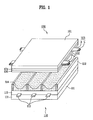
- FIG. 1 is a schematic perspective view of a conventional plasma display panel.
- a plurality of pairs of retaining electrodes each of which includes a scan electrode 102 and a sustain electrode 103, are arranged on a front glass 101, serving as a display plane, on which an image is displayed, of a front substrate 100 of the plasma display panel.
- a plurality of address electrodes 113 are arranged on a rear glass 111 of a rear substrate 110 in such a manner that the address electrodes 113 intersect the pairs of the retaining electrodes.
- the rear substrate 110 is connected to the front substrate 100 in parallel under the condition that the rear substrate 110 and the front substrate 100 are spaced from each other by a designated distance.
- the above conventional plasma display panel is manufactured through a glass-manufacturing process, a front substrate-manufacturing process, a rear substrate-manufacturing process, and an assembling process.
- the front substrate-manufacturing process includes forming scan electrodes and sustain electrodes on a front glass, forming an upper dielectric layer for limiting discharge current of the scan and sustain electrodes and insulating pairs of the scan and sustain electrodes from each other, and forming a protection layer on the upper dielectric by depositing magnesium oxide for facilitating the discharge condition
- the rear substrate-manufacturing process includes forming address electrodes on a rear glass, forming a lower dielectric layer for protecting the address electrodes, forming barrier ribs on the upper surface of the lower dielectric layer for dividing discharge cells from each other, and forming a fluorescent material layer on regions between the barrier ribs for emitting visible rays.
- the above method for manufacturing the plasma display panel has problems, as follows.
- the barrier ribs serve to prevent electrical and optical crosstalk between the discharge cells, and are important to increase the display quality and the light-emitting efficiency of the plasma display panel.
- PDPs are developed towards large-size and high-definition trends, various researches on the barrier ribs have now been made.
- a barrier rib material is formed on the lower dielectric layer by printing a barrier rib paste or laminating a barrier rib green sheet on the lower dielectric layer, and the barrier ribs are obtained by a sanding, etching, or photosensitive method.
- the formation of a black top on the upper surfaces of the barrier ribs is added to this barrier rib-forming process. That is, a black top material and a dry film resist (DFR) layer are sequentially formed on the barrier rib material on the lower dielectric layer. Then, after the barrier ribs and black tops are formed by a sanding method, the DFR layer is removed.
- DFR dry film resist
- the above conventional barrier rib-forming process additionally requires separate materials and steps. Further, since the width of the pattern of the black tops cannot be adjusted, the luminance of the plasma display panel is deteriorated. Moreover, the side surfaces of the black tops are exposed to an etchant during the exposing and developing processes.
- the present invention is directed to a black top green sheet, a plasma display panel, and a method for manufacturing the same.
- One object of the present invention is to provide a plasma display panel, in which a process for forming barrier ribs and black tops is simplified, and a method for manufacturing the same.
- a method for manufacturing a plasma display panel includes forming a barrier rib material on a lower plate, on which address electrodes and a dielectric are provided; forming a black top material comprising a photosensitive substance on the barrier rib material; patterning the black top material to form black tops; and patterning the barrier rib material using the black tops as a mask to form barrier ribs.
- a plasma display panel includes upper and lower plates, which face each other; barrier ribs formed on the lower plate and comprising a white material; and black tops formed on the barrier ribs and having a narrower width than that of the barrier ribs.
- a black top green sheet includes a photosensitive black paste layer, which has viscosity when it is not exposed to light, and loses the viscosity when it is exposed to the light; and first and second protection films provided on the upper and lower surfaces of the black paste layer.
- a method for manufacturing a plasma display panel includes preparing a black top green sheet, the viscosity of which is changed when it is exposed to light; selectively exposing the black top green sheet to light according to regions corresponding to barrier ribs; and bonding non-exposed portions of the black top green sheet to the barrier ribs provided on a lower plate.
- a plasma display panel in another aspect of the present invention, includes upper and lower plates, which face each other; and black tops formed on barrier ribs in the lower plate, and comprising a photosensitive substance, which maintains viscosity when it is not exposed to light, and loses the viscosity when it is exposed to the light.
- a method for manufacturing a plasma display panel includes forming a barrier rib material on a lower plate, on which address electrodes and a dielectric are provided; forming a black top material comprising a photosensitive substance on the barrier rib material; and forming barrier ribs and black tops by exposing the barrier rib material and the black top material to light and developing the barrier rib material and the black top material.
- a method for manufacturing a plasma display panel includes forming a multi-layer green sheet comprising a photosensitive substance on a lower plate, on which address electrodes and a dielectric are provided; and forming barrier ribs and black tops by exposing the multi-layer green sheet to light and developing the multi-layer green sheet.
- FIG. 1 is a schematic perspective view of a conventional plasma display panel
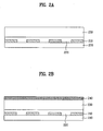
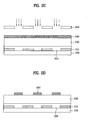
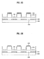
- FIGS. 2A to 2H are sectional views illustrating a method for manufacturing a plasma display panel in accordance with a first embodiment of the present invention
- FIG. 3 is a sectional view of a black top green sheet in accordance with the present invention.
- FIGS. 4A to 4D are sectional views illustrating a method for manufacturing a plasma display panel in accordance with a second embodiment of the present invention.
- FIGS. 5A to 5D are sectional views illustrating a method for manufacturing a plasma display panel in accordance with a third embodiment of the present invention.
- FIGS. 6A to 6C are sectional views illustrating a method for manufacturing a plasma display panel in accordance with a fourth embodiment of the present invention.
- FIGS. 2A to 2H are views illustrating a method for manufacturing a plasma display panel in accordance with a first embodiment of the present invention.
- the method for manufacturing the plasma display panel in accordance with the first embodiment will be described.
- a lower dielectric 220 is formed on a lower glass 200, on which address electrodes 210 are provided. Then, a barrier rib material 230 is formed on the lower dielectric 220. In order to improve the luminance of the plasma display panel, the barrier rib material 230 preferably includes a white substance.
- a black top material 240 is formed on the barrier rib material 230.
- the barrier rib material 240 is manufactured in a green sheet type and laminated on the lower glass 200, or is manufactured in a paste type and printed on the lower glass 200.
- the black top material 240 preferably includes a photosensitive substance. More preferably, the photosensitive substance is a photosensitive monomer.
- the black top material 240 is patterned.
- ultraviolet rays are selectively irradiated onto the black top material 240 using a mask 250.
- portions of the black top material 240, which are exposed to the ultraviolet rays, are removed by a developing process, thus forming black tops 260, as shown in FIG. 2D.
- the barrier rib material 230 is patterned using the black tops 260 as a mask.
- the patterning of the barrier rib material 230 is achieved by an etching or sanding method.
- the black tops 260 are not damaged during the patterning of the barrier rib material 230 using the etching or sanding method.
- FIG. 2F illustrates barrier ribs 270 obtained by patterning the barrier rib material 230.
- fluorescent materials 280 are applied to the upper surface of the dielectric 220 and the side surfaces of the barrier ribs 270.
- Red (R), Green (G), and Blue (B) fluorescent materials 280 are alternately applied, and sub-pixels, on which the R, G, and B fluorescent materials 280 are respectively formed, form one pixel.
- the fluorescent materials 280 and the black tops 260 are simultaneously baked.
- the width of the black tops 260 is contracted to be narrower than that of the barrier ribs 270, and preferably to be 80 ⁇ 90% of that of the barrier ribs 270.
- the contraction of the width of the black tops 260 is caused by the composition of the black top material 240.
- the black top material 240 further includes a glass composite, a binder, and an initiator. The contraction degree of the black tops 260 during the baking process is varied according to the amount of the binder.
- the amount of the binder in the black top material 260 is preferably 30 ⁇ 50% of the total amount of the black top material 260.
- the plasma display panel manufactured by the above method has the black tops formed on the white barrier ribs, and thus has an improved contrast. As described above, the width of the black tops is adjusted, thereby preventing the deterioration of the luminance of the plasma display panel.
- the plasma display panel has the black tops including the photosensitive substance formed on the barrier ribs and does not require a DFR layer, thus preventing the addition of steps of the manufacturing process. Further, since the fluorescent materials and the black tops are simultaneously baked, it is possible to simultaneously achieve the removal of organic matters and the adjustment of the width of the black tops.
- FIG. 3 is a sectional view of a black top green sheet in accordance with the present invention.
- the black top green sheet of the present invention will be described.
- the black top green sheet of the present invention comprises a black paste layer 300, and first and second films 310 and 320 provided at both surfaces of the black paste layer 300.
- the black paste layer 300 is made of a black-colored material having a light absorbing property, the viscosity of which is changed by ultraviolet rays irradiated thereonto. That is, the black paste layer 300 preferably includes a photosensitive material, which has the viscosity with the first and second films 310 and 320, and is hardened by ultraviolet rays irradiated thereonto and loses the viscosity. More preferably, the black paste layer 300 further includes a black inorganic pigment, an organic binder made of an organic matter, and a solvent.
- the above photosensitive material is a photosensitive polymer, which includes a polymer and a photosensitizer. Since the photosensitive material has a negative property, the bonding force of the photosensitive is increased when it is exposed to light.
- the first and second films 310 and 320 are formed on the upper and lower surfaces of the black paste layer 300, and serve as protection films. In order to perform an exposing process, which will be described later, preferably, at least one of the first and second films 310 and 320 is transparent. Further, in order to easily attach and remove the first and second films 310 and 320 to and from the black paste layer 300, preferably, the first and second films 310 and 320 have surface characteristics, which reduce the viscosity of the black paste layer 300.
- the above black top green sheet serves as not only a material for forming black tops on the surface of barrier ribs, but also a black matrix. Further, the black top green sheet may serve various purposes for forming a black pattern layer. Preferably, the black top green sheet is first patterned and then formed on the surface of structures, such as barrier ribs, rather than is first formed directly on the upper surface of the structures and then patterned. That is, although structures, such as the black tops, to which a black material layer is applied, are complicated and the thickness of the layer is limited so that the layer cannot be formed by a printing method, the black top green sheet is used to easily form the black material layer having a small thickness. Particularly, in case that a layer to be formed has a fine thickness or cannot be patterned by etching, the black top green sheet is useful.
- FIGS. 4A to 4D are sectional views illustrating a method for manufacturing a plasma display panel in accordance with a second embodiment of the present invention.
- the method for manufacturing the plasma display panel in accordance with the second embodiment will be described.
- the black top green sheet as shown in FIG. 3, is prepared. Then, as shown in FIG. 4A, the black top green sheet is selectively exposed to light. Specifically, a mask 400 is located on the black top green sheet in such a manner that portions of the black top green sheet corresponding to barrier ribs are not exposed to the light, and then the black top green sheet is selectively exposed to the light. Since the black paste layer 300 includes the organic binder and the solvent so that the viscosity of the black paste layer 300 is maintained, the black paste layer 300 is dried and hardened in a subsequent process, thus being decreased in terms of volume. Accordingly, in consideration of the decrease of the volume of the black paste layer 300, the mask 400 preferably has a pattern, which causes portions of the black green sheet having a width wider than that of the upper surface of the barrier ribs not to be exposed to the light.
- the bonding force between molecules of the polymer in the exposed portions 300' of the black paste layer 300 is increased, and the exposed portions 300' of the black paste layer 300 lose the viscosity.
- other portions of the black paste layer 300 i.e., non-exposed portions of the black paste layer 300, maintain the viscosity.
- a lower plate 410 provided with barrier ribs 420 is prepared, and the black top green sheet, from which the second protection film 320 is removed, is arranged on the lower plate 410. Then, the barrier ribs 420 and the black paste layer 300 are compressed against each other, and preferably compressed against each other using a roller.
- the first film 310 and the exposed portions 300 of the black paste layer 300 attached to the first film 00 are separated from the lower plate 410.
- the non-exposed portions of the black paste layer 300 are firmly compressed against the barrier ribs 420, thus not separated from the lower plate 410.
- the black tops in order to improve the white ray reflecting property of the barrier ribs and the improvement of the contrast due to the black tops formed on the upper surfaces of the barrier ribs, the black tops preferably have a thickness of below 30% of that of the barrier ribs.
- Processes for forming other parts except for the process for forming the barrier ribs and the black tops in the method of this embodiment are the same as those in the conventional method. Accordingly, it is possible to easily separate the exposed portions of the black paste layer from the lower plate, while increasing the viscosity of the non-exposed portions of the black paste layer with the barrier ribs. Further, since the black paste layer is selectively exposed to light according to the pattern of the barrier ribs, and is then transcribed onto the barrier ribs, it is possible to adjust the thickness of the black paste layer. Moreover, the barrier ribs are not exposed to an etchant for a long period of time, thus not being distorted.
- FIGS. 5A to 5D are sectional views illustrating a method for manufacturing a plasma display panel in accordance with a third embodiment of the present invention.
- the method for manufacturing the plasma display panel in accordance with the third embodiment will be described.
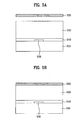
- a barrier rib material 550 is prepared, and is formed on a lower glass 510, on which address electrodes 530 and a dielectric 540 are sequentially provided.
- the barrier rib material 550 is manufactured in a green sheet type and laminated on the lower glass 510, or is manufactured in a paste type and formed on the lower glass 510 by printing or coating.
- the barrier rib material 550 is obtained by mixing a mixture, obtained by mixing several tens of % of an oxide in a powdery state, such as Al 2 O 3 , for improving reflection property and controlling permittivity with PbO or non-PbO glass powder, with an organic solvent.
- a black top material 555 is formed on the barrier rib material 550.
- the black top material 555 includes a photosensitive substance.
- the black top material 555 is manufactured in a green sheet type and laminated on the barrier rib material 550, or is manufactured in a paste type and formed on the barrier rib material 550 by printing or coating.
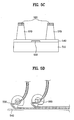
- the barrier rib material 550 and the black top material 555 are exposed to light, and are developed, thus forming barrier ribs 570 and black tops 580.
- a mask is aligned on the upper surface of the black top material 555.
- the mask has light shielding portions and light transmitting portions, which are alternately formed at the same interval.
- the light transmitting portions transmit light so that the light is irradiated onto the barrier rib material 550 under the light transmitting portions and hardens the barrier rib material 550, and the light shielding portions shield light so that the light is not irradiated onto the barrier rib material 550 under the light shielding portions.
- the barrier ribs 570 and the black tops 580 are formed by developing the barrier rib material 550 and the black top material 555.
- the above exposure and development is performed by a sanding, etching, or photosensitive method, thus removing the barrier rib material 550 and the black top material 555 under the light shielding portions.
- the barrier rib material 550 and the black top material 555 are simultaneously formed using two coating heads, as shown in FIG. 5D.
- FIGS. 6A to 6C are sectional views illustrating a method for manufacturing a plasma display panel in accordance with a fourth embodiment of the present invention.
- the method for manufacturing the plasma display panel in accordance with the fourth embodiment will be described.
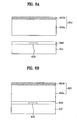
- a multi-layer green sheet 650 is prepared.
- the multi-layer green sheet 650 includes a barrier rib material layer 650a, and a black top material layer 650b including a photosensitive substance. That is, in the fourth embodiment, the barrier rib material and the black top material of the third embodiment are combined into a single green sheet, and the green sheet is formed on a lower plate of the plasma display panel. Accordingly, preferably, the multi-layer green sheet 650 of the fourth embodiment includes components of the barrier rib material and the black top material of the third embodiment.
- the multi-layer green sheet 650 is formed on a lower glass 610, on which address electrodes 630 and a dielectric 640 are sequentially provided.
- the multi-layer green sheet 650 is laminated on the lower glass 610.
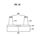
- the multi-layer green sheet 650 is exposed to light, and is developed, thus forming barrier ribs and black tops.
- the multi-layer green sheet 650 is selectively exposed to the light using a mask in the same manner as the method of the third embodiment.
- barrier ribs 670 and black tops 680 are formed by developing the multi-layer green sheet 550.
- the above exposure and development is performed by a sanding, etching, or photosensitive method.
- the black tops and the barrier ribs are simultaneously formed without the formation of the conventional DFR layer, thus reducing production costs of the plasma display panel and shortening the manufacturing process of the plasma display panel.
- the plasma display panel manufactured by the above method uses barrier ribs and a black top material including a photosensitive substance, thus simplifying a process for manufacturing the plasma display panel and reducing the production costs of the plasma display panel.
- the barrier ribs are made of a white material
- the black tops, which are formed on the barrier ribs reduce the reflectance of external light, thus maximizing the contrast of the plasma display panel.
- the above method may be applied to other display panels, such as an OLED and an LCD, as well as a plasma display panel.
Landscapes
- Physics & Mathematics (AREA)
- Engineering & Computer Science (AREA)
- Plasma & Fusion (AREA)
- Electromagnetism (AREA)
- Manufacturing & Machinery (AREA)
- Gas-Filled Discharge Tubes (AREA)
Applications Claiming Priority (3)
| Application Number | Priority Date | Filing Date | Title |
|---|---|---|---|
| KR1020050061741A KR100710334B1 (ko) | 2005-07-08 | 2005-07-08 | 플라즈마 디스플레이 패널의 제조방법 |
| KR1020050082618A KR100774182B1 (ko) | 2005-09-06 | 2005-09-06 | 플라즈마 디스플레이 패널 및 그 제조방법 |
| KR1020050106134A KR100741776B1 (ko) | 2005-11-07 | 2005-11-07 | 블랙층 그린시트 및 이를 이용한 디스플레이 패널 제조방법 |
Publications (2)
| Publication Number | Publication Date |
|---|---|
| EP1742245A2 true EP1742245A2 (de) | 2007-01-10 |
| EP1742245A3 EP1742245A3 (de) | 2009-01-21 |
Family
ID=37075791
Family Applications (1)
| Application Number | Title | Priority Date | Filing Date |
|---|---|---|---|
| EP06291128A Withdrawn EP1742245A3 (de) | 2005-07-08 | 2006-07-07 | Schwarze Grünfolienoberschicht, Plasma-Anzeigetafel und Verfahren zur deren Herstellung |
Country Status (3)
| Country | Link |
|---|---|
| US (1) | US20070013308A1 (de) |
| EP (1) | EP1742245A3 (de) |
| JP (1) | JP2007019028A (de) |
Cited By (1)
| Publication number | Priority date | Publication date | Assignee | Title |
|---|---|---|---|---|
| EP1783805A3 (de) * | 2005-11-07 | 2009-01-21 | LG Electronics Inc. | Grünschicht für schwarze Schichten, Plasmaanzeigetafeln mit dieser Grünschicht und Verfahren zur Herstellung dieser Plasmaanzeigetafeln |
Families Citing this family (2)
| Publication number | Priority date | Publication date | Assignee | Title |
|---|---|---|---|---|
| EP3528049A1 (de) * | 2018-02-20 | 2019-08-21 | ASML Netherlands B.V. | Metrologieverfahren und -vorrichtung mit erhöhter bandbreite |
| CN113140577B (zh) * | 2021-04-21 | 2024-01-26 | 滁州惠科光电科技有限公司 | 一种阵列基板制备方法、阵列基板及显示面板 |
Family Cites Families (5)
| Publication number | Priority date | Publication date | Assignee | Title |
|---|---|---|---|---|
| US5909083A (en) * | 1996-02-16 | 1999-06-01 | Dai Nippon Printing Co., Ltd. | Process for producing plasma display panel |
| KR100477603B1 (ko) * | 2002-05-28 | 2005-03-18 | 엘지전자 주식회사 | 플라즈마 디스플레이 패널의 격벽 제조방법 |
| KR20030093549A (ko) * | 2002-06-03 | 2003-12-11 | 엘지전자 주식회사 | 플라즈마 디스플레이 패널의 격벽 제조방법 |
| KR20040104790A (ko) * | 2003-06-04 | 2004-12-13 | 엘지전자 주식회사 | 블랙 레지스트를 이용한 플라즈마 디스플레이 패널의 격벽및 그 제조방법 |
| JP2007019019A (ja) * | 2005-07-05 | 2007-01-25 | Lg Electronics Inc | プラズマディスプレイパネルの製造方法 |
-
2006
- 2006-07-07 US US11/482,192 patent/US20070013308A1/en not_active Abandoned
- 2006-07-07 EP EP06291128A patent/EP1742245A3/de not_active Withdrawn
- 2006-07-10 JP JP2006189124A patent/JP2007019028A/ja not_active Withdrawn
Cited By (1)
| Publication number | Priority date | Publication date | Assignee | Title |
|---|---|---|---|---|
| EP1783805A3 (de) * | 2005-11-07 | 2009-01-21 | LG Electronics Inc. | Grünschicht für schwarze Schichten, Plasmaanzeigetafeln mit dieser Grünschicht und Verfahren zur Herstellung dieser Plasmaanzeigetafeln |
Also Published As
| Publication number | Publication date |
|---|---|
| US20070013308A1 (en) | 2007-01-18 |
| EP1742245A3 (de) | 2009-01-21 |
| JP2007019028A (ja) | 2007-01-25 |
Similar Documents
| Publication | Publication Date | Title |
|---|---|---|
| KR20030036909A (ko) | 플라즈마 디스플레이 패널과 그 제조방법 | |
| JP3860673B2 (ja) | プラズマディスプレイパネルおよびその製造方法 | |
| KR100524302B1 (ko) | 플라즈마 디스플레이 패널 및 그 제조방법 | |
| EP1742245A2 (de) | Schwarze Grünfolienoberschicht, Plasma-Anzeigetafel und Verfahren zur deren Herstellung | |
| JPH09115452A (ja) | プラズマディスプレイパネルの障壁構造 | |
| JP4161479B2 (ja) | プラズマディスプレイ用部材およびプラズマディスプレイの製造方法 | |
| EP1912243B1 (de) | Plasmaanzeigetafel und Verfahren zu ihrer Herstellung | |
| US20090058298A1 (en) | Plasma display panel and method of fabricating the same | |
| JP2002056775A (ja) | プラズマディスプレイパネル用基板の製造方法、プラズマディスプレイパネル用基板及びプラズマディスプレイパネル | |
| JP4604752B2 (ja) | フラットディスプレイパネルの製造に用いるフォトマスクおよびフラットディスプレイパネルの製造方法 | |
| US7722423B2 (en) | Method of manufacturing plasma display panel with concave barrier wall portion | |
| US20070013307A1 (en) | Method for manufacturing plasma display panel | |
| KR20050008721A (ko) | 플라즈마 디스플레이 패널의 제조 방법 및 플라즈마디스플레이 패널 | |
| KR20050032849A (ko) | 플라즈마 디스플레이 패널 및 그 제조방법 | |
| US20080297049A1 (en) | Plasma display panel and method for fabricating the same | |
| KR100741776B1 (ko) | 블랙층 그린시트 및 이를 이용한 디스플레이 패널 제조방법 | |
| KR100743070B1 (ko) | 얇은 블랙립을 구비하는 플라즈마 디스플레이 패널 및 그의제조 방법 | |
| KR100467076B1 (ko) | 플라즈마 디스플레이 패널의 격벽 제조방법 | |
| US20070103075A1 (en) | Green sheet for black layers, plasma display panels using the green sheet and methods for fabricating the plasma display panels | |
| JP2006294501A (ja) | プラズマディスプレイ用部材 | |
| KR100741775B1 (ko) | 플라즈마 디스플레이 패널의 전극 형성 방법 | |
| JP2002216640A (ja) | ガス放電表示装置およびその製造方法 | |
| KR100560511B1 (ko) | 플라즈마 디스플레이 패널의 제조 방법 | |
| KR100323697B1 (ko) | 플라즈마 디스플레이 패널의 블랙매트릭스 형성방법과 그 구조 | |
| JP2001176401A (ja) | プラズマディスプレイ用部材およびその製造方法ならびにプラズマディスプレイ |
Legal Events
| Date | Code | Title | Description |
|---|---|---|---|
| PUAI | Public reference made under article 153(3) epc to a published international application that has entered the european phase |
Free format text: ORIGINAL CODE: 0009012 |
|
| 17P | Request for examination filed |
Effective date: 20060717 |
|
| AK | Designated contracting states |
Kind code of ref document: A2 Designated state(s): AT BE BG CH CY CZ DE DK EE ES FI FR GB GR HU IE IS IT LI LT LU LV MC NL PL PT RO SE SI SK TR |
|
| AX | Request for extension of the european patent |
Extension state: AL BA HR MK YU |
|
| RIC1 | Information provided on ipc code assigned before grant |
Ipc: H01J 17/49 20060101ALI20080923BHEP Ipc: H01J 9/20 20060101ALI20080923BHEP Ipc: H01J 9/24 20060101AFI20061026BHEP Ipc: H01J 9/227 20060101ALI20080923BHEP |
|
| PUAL | Search report despatched |
Free format text: ORIGINAL CODE: 0009013 |
|
| AK | Designated contracting states |
Kind code of ref document: A3 Designated state(s): AT BE BG CH CY CZ DE DK EE ES FI FR GB GR HU IE IS IT LI LT LU LV MC NL PL PT RO SE SI SK TR |
|
| AX | Request for extension of the european patent |
Extension state: AL BA HR MK RS |
|
| STAA | Information on the status of an ep patent application or granted ep patent |
Free format text: STATUS: THE APPLICATION HAS BEEN WITHDRAWN |
|
| 18W | Application withdrawn |
Effective date: 20090717 |