EP1744143A1 - Rastersondenmikroskopsonde und herstellungsverfahren dafür sowie rastersondenmikroskop und anwendungsverfahren dafür sowie nadelähnliches element und herstellungsverfahren dafür sowie elektronenelement und herstellungsverfahren dafür sowie ladungsdichtewellenquantum-phasenmikroskop und ladungsdichtewellenquantum-interferometer - Google Patents
Rastersondenmikroskopsonde und herstellungsverfahren dafür sowie rastersondenmikroskop und anwendungsverfahren dafür sowie nadelähnliches element und herstellungsverfahren dafür sowie elektronenelement und herstellungsverfahren dafür sowie ladungsdichtewellenquantum-phasenmikroskop und ladungsdichtewellenquantum-interferometer Download PDFInfo
- Publication number
- EP1744143A1 EP1744143A1 EP05736881A EP05736881A EP1744143A1 EP 1744143 A1 EP1744143 A1 EP 1744143A1 EP 05736881 A EP05736881 A EP 05736881A EP 05736881 A EP05736881 A EP 05736881A EP 1744143 A1 EP1744143 A1 EP 1744143A1
- Authority
- EP
- European Patent Office
- Prior art keywords
- substrate
- needle
- crystal
- probe
- point
- Prior art date
- Legal status (The legal status is an assumption and is not a legal conclusion. Google has not performed a legal analysis and makes no representation as to the accuracy of the status listed.)
- Withdrawn
Links
Images





Classifications
-
- G—PHYSICS
- G01—MEASURING; TESTING
- G01Q—SCANNING-PROBE TECHNIQUES OR APPARATUS; APPLICATIONS OF SCANNING-PROBE TECHNIQUES, e.g. SCANNING PROBE MICROSCOPY [SPM]
- G01Q70/00—General aspects of SPM probes, their manufacture or their related instrumentation, insofar as they are not specially adapted to a single SPM technique covered by group G01Q60/00
- G01Q70/16—Probe manufacture
-
- G—PHYSICS
- G01—MEASURING; TESTING
- G01Q—SCANNING-PROBE TECHNIQUES OR APPARATUS; APPLICATIONS OF SCANNING-PROBE TECHNIQUES, e.g. SCANNING PROBE MICROSCOPY [SPM]
- G01Q70/00—General aspects of SPM probes, their manufacture or their related instrumentation, insofar as they are not specially adapted to a single SPM technique covered by group G01Q60/00
- G01Q70/06—Probe tip arrays
-
- B—PERFORMING OPERATIONS; TRANSPORTING
- B82—NANOTECHNOLOGY
- B82Y—SPECIFIC USES OR APPLICATIONS OF NANOSTRUCTURES; MEASUREMENT OR ANALYSIS OF NANOSTRUCTURES; MANUFACTURE OR TREATMENT OF NANOSTRUCTURES
- B82Y15/00—Nanotechnology for interacting, sensing or actuating, e.g. quantum dots as markers in protein assays or molecular motors
-
- B—PERFORMING OPERATIONS; TRANSPORTING
- B82—NANOTECHNOLOGY
- B82Y—SPECIFIC USES OR APPLICATIONS OF NANOSTRUCTURES; MEASUREMENT OR ANALYSIS OF NANOSTRUCTURES; MANUFACTURE OR TREATMENT OF NANOSTRUCTURES
- B82Y35/00—Methods or apparatus for measurement or analysis of nanostructures
-
- G—PHYSICS
- G01—MEASURING; TESTING
- G01Q—SCANNING-PROBE TECHNIQUES OR APPARATUS; APPLICATIONS OF SCANNING-PROBE TECHNIQUES, e.g. SCANNING PROBE MICROSCOPY [SPM]
- G01Q70/00—General aspects of SPM probes, their manufacture or their related instrumentation, insofar as they are not specially adapted to a single SPM technique covered by group G01Q60/00
- G01Q70/08—Probe characteristics
- G01Q70/10—Shape or taper
- G01Q70/12—Nanotube tips
Definitions
- the present invention relates to a scanning probe microscope probe and manufacturing method therefor, a scanning probe microscope and using method therefor, a needle-like body and manufacturing method therefor, an electronic device and manufacturing method therefor, a charge density wave quantum phase microscope, and a charge density wave quantum interferometer.
- the present invention is suitably usable for production of a novel device from a charge density wave nano-structure, determination of a biomolecular structure, surface inspection of various substances including superconducting ones, and a semiconductor device, etc.
- conduction electrons in an electric conductor such as a metal can be macroscopically quantum-coherent with each other.
- the conduction electrons can be macroscopically quantum-coherent with each other only in two of the three states, namely, in the states of superconductivity and charge density wave (CDW), unless handled from outside.
- a CDW body shows a phase transition at room temperature
- a device and measuring device, utilizing the CDW macroscopic quantum phase are practically higher in potential than the semiconductor technology and have been attracting more and more attention.
- CDW three-terminal electric field/current driving device, femtosecond-speed memory device, etc. have been worked out and proved each as a new quantum functional device having a new effect (as in Appl. Phys. Lett. 80, 871 (2002 ), for example).
- the scanning probe microscope is an important tool for the nano-science and nano-technology, and is widely applied to surface inspection of various substances, development of materials and devices, etc.
- the conventional scanning probe microscope could not be any effective tool for studying the nano-scale nonuniform superconducting state. Therefore, there has been demanded a new tool, but any such effective tool has not yet been proposed.
- Another object of the present invention is, more generally, to provide a variety of needle-like bodies including the above-mentioned scanning probe microscope probe and manufacturing methods therefor, and an electronic device and manufacturing method therefor.
- the other object of the present invention is to provide a charge density wave quantum interferometer capable of measuring a local electric field with a high precision by actively utilizing macroscopic quantum phase information on a charge density wave.
- Further object of the present invention is to provide a scanning probe microscope suitably usable for study of the nano-scale nonuniform superconducting state, observation of a flux-line lattice, study of the state of electrons within a magnetic flux, and observation of an image of specimen surface irregularities, and use of the scanning probe microscope.
- the Inventors of the present invention actively prepared a theoretically designed CDW nano-structure from the standpoint of the materials science, and tried to make clear external stimulus-caused changes in electrical, elastic and optical properties of the materials of the nano-structure with an intention to apply the nano-structure effectively in various fields of industry.
- the Inventors intended to develop a smaller, higher-performance microscope which can actively utilize the macroscopic quantum phase information on CDW.
- Such a microscope is an indispensable tool for production of a device from a CDW nano-structure, and also it will be much contributed to determination of a biomolecular structure represented by DNA, development of a quantum computer that uses quantum phase information, etc.
- CDW is normally pinned under the influence of impurities and specimen end. When applied with an electric field larger than a threshold field, however, CDW will slide and contribute to electric conduction. The CDW sliding is a collective translation of electrons, which is a characteristic phenomenon of low-order conductors. When CDW slides through a pinning potential, there will develop an AC current having a frequency proportional to a DC current component carried by CDW, that is, a narrow-band signal (NBS) (also called “narrow-band noise (NBN)"). On the consumption that an excess current portion flowing when an electric field larger than the threshold one is applied is J CDW and the frequency of NBS is ⁇ NBS , ⁇ NBS ⁇ J CDW .
- NBS narrow-band signal
- a change in threshold electric field can be determined with a high precision through measurement of the frequency ⁇ NBS of NBS. Since the threshold electric field is changed by a slight stress developed in a CDW crystal, just connecting electrodes to a CDW needle to measure NBS can provide a high-precision microscope higher in functionality than an atomic force microscope (AFM). For example, use of a 100 nm-long CDW needle-like crystal makes it possible to provide a microscope having an optical resolution of 1 pm with the sensitivity of a frequency meter used being 1 Hz. In AFM, a shift of a probe of a cantilever is detected by irradiating the cantilever with laser light. However, since the above CDW microscope requires no such an optical system, so it can be designed very small. Thus, the CDW microscope is largely advantageous because it can be introduced directly into a living body like a syringe.
- the Inventors made a variety of experiments for growing a needle-like crystal at the tip of a cone formed from Si, for example, by using irradiation of an energy beam such as an electron beam, and found the fact that even if the energy beam is irradiated to the tip of a cone having a raw material deposited on the surface thereof, it is difficult to grow a needle-like crystal at the cone tip, while irradiation of the energy beam to a point, apart from the tip, of the cone permits to easily grow a needle-like crystal at the cone tip.
- an energy beam such as an electron beam
- the Inventors found that selective irradiation of an energy beam such as an electron beam to the surface of a substrate to recrystallize the beam-irradiated point of the substrate permits to grow a needle-like crystal in a form in which the substrate and crystal are contiguous to each other.
- Growing a CDWneedle-like crystal with these techniques and using the needle-like crystal as a probe make it possible to provide a CDW probe microscope.
- growing a needle-like crystal of any other material and using the needle-like crystal as a probe permit to implement various types of scanning probe microscopes.
- growing a needle-like semiconductor crystal, for example, by these methods permits to provide a micro semiconductor device.
- the Inventors found that for implementation of an effective tool for study of the nano-scale nonuniform superconducting state, it is effective to use, as a scanning probe microscope probe, a pressure-induced superconducting substance having superconductivity susceptive to a pressure and whose superconducting state can thus be controlled by applying a small pressure.
- the present invention was worked out based on the above Inventors' findings.
- a scanning probe microscope probe produced by depositing a raw material on the surface of a cone- or blade-shaped substrate and growing a needle-like crystal by using the raw material by irradiating an energy beam to a point on the substrate at a predetermined distance along the side surface from the substrate tip under such conditions as not to melt the substrate.
- a manufacturing method for a scanning probe microscope probe wherein a raw material is deposited on the surface of a cone-or blade-shaped substrate and a needle crystal is grown by using the raw material by irradiating an energy beam to a point on the substrate at a predetermined distance along the side surface from the substrate tip under such conditions as not to melt the substrate.
- a scanning probe microscope including a probe produced by depositing a raw material on the surface of a cone- or blade-shaped substrate and growing a needle-like crystal by using the raw material by irradiating an energy beam to a point on the substrate at a predetermined distance along the side surface from the substrate tip under such conditions as not to melt the substrate.
- a scanning probe microscope probe produced by supplying a raw material to the surface of a cone- or blade-shaped substrate and growing a needle-like crystal by using the raw material by irradiating an energy beam to a point on the substrate at a predetermined distance along the side surface from the substrate tip under such conditions as not to melt the substrate.
- a manufacturing method for a scanning probe microscope probe wherein a raw material is supplied to the surface of a cone-or blade-shaped substrate and a needle-like crystal is grown by using the rawmaterial by irradiating an energy beam to a point on the substrate at a predetermined distance along the side surface from the substrate tip under such conditions as not to melt the substrate.
- a scanning probe microscope including a probe produced by supplying a raw material to the surface of a cone- or blade-shaped substrate and growing a needle-like crystal by using the raw material by irradiating an energy beam to a point on the substrate at a predetermined distance along the side surface from the substrate tip under such conditions as not to melt the substrate.
- a scanning probe microscope probe produced by depositing a first rawmaterial on the surface of a cone- or blade-shaped substrate, supplying a second rawmaterial to the surface and growing a needle-like crystal by using the first and second raw materials by irradiating an energy beam to a point on the substrate at a predetermined distance along the side surface from the substrate tip under such conditions as not to melt the substrate.
- a manufacturing method for a scanning probe microscope probe wherein a first raw material is deposited on the surface of a cone- or blade-shaped substrate, a second raw material is supplied to the surface and a needle-like crystal is grown by using the first and second raw materials by irradiating an energy beam to a point on the substrate at a predetermined distance along the side surface from the substrate tip under such conditions as not to melt the substrate.
- a scanning probe microscope including a probe produced by depositing a first raw material on the surface of a cone- or blade-shaped substrate, supplying a second raw material to the surface and growing a needle-like crystal by using the first and second raw materials by irradiating an energy beam to a point on the substrate at a predetermined distance along the side surface from the substrate tip under such conditions as not to melt the substrate.
- the above first to ninth aspects of the present invention uses a substrate formed from a material whose melting point is so high that it will not be softened when irradiated with an energy beam, for example, 800°C or higher.
- the substrate may have a triangular pyramid shape or quadrangular pyramid shape in addition to the circular cone shape. Namely, its sectional area has only to be smaller toward the tip.
- the energy beam may be, for example, an electron beam, ion beam or laser beam.
- the laser beam may be laser beam generated by excimer laser, YAG laser, Ar laser or the like.
- the sectional shape of the energy beam is not limited to any special one but it may be circular, elliptic or rectangular.
- the energy beam should have a flat rectangular sectional shape.
- the energy beam By irradiating the energy beam over the plurality of conical portions, needle-like crystals can collectively be grown on the conical portions.
- An energy beam having such a flat rectangular sectional shape can easily be obtained by shaping a laser beam through an optical system including a lens, etc.
- the raw material can be deposited or supplied by any of the deposition methods such as the vacuum evaporation, sputtering, chemical vapor deposition (CVD), metalorganic chemical vapor deposition (MOCVD), molecular beam epitaxy (MBE) and the like or by an appropriate combination of them.
- the laser beam When the laser beam is irradiated, generally, between an energy beam-irradiated point and tip of the substrate tip, there is a temperature gradient of above 10°C/ ⁇ m and below 100°C/ ⁇ m, starting at the substrate tip (at the lowest temperature).
- the thickness of the needle-like crystal is determined as necessary, but it is generally above 5 nm and below 1 ⁇ m.
- the needle-like crystal should preferably be grown in vacuum or in hydrogen gas in order to prevent oxidation.
- the needle-like crystal is formed from MX p (where M is at least one element selected from a group of Ta and Nb, X is at least one element selected from a group of S, Se and Te, and 1.8 ⁇ p ⁇ 2.2), MX q (where M is at least one element selected from a group of Ta and Nb, X is at least one element selected from a group of S, Se and Te, and 2.7 ⁇ q ⁇ 3.3) or MX r (where M is at least one element selected from a group of Ta and Nb, X is at least one element selected from a group of S, Se and Te, and 3.6 ⁇ r ⁇ 4.4) .
- MX p is TaSe 2 or TaS 2
- MX q is NbSe 3 or NbS 3
- MX r is NbTe 4 or the like.
- the needle-like crystal may be of a metal such as Ni or Cu or a superconducting material (oxide superconductor or the like).
- a manufacturing method for a needle-like body wherein a raw material is deposited on the surface of a cone- or blade-shaped substrate and a needle-like crystal is grown by using the raw material by irradiating an energy beam to a point on the substrate at a predetermined distance along the side surface from the substrate tip under such conditions as not to melt the substrate.
- a manufacturing method for a needle-like body wherein a raw material is supplied to the surface of a cone- or blade-shaped substrate and a needle-like crystal is grown by using the raw material by irradiating an energy beam to a point on the substrate at a predetermined distance along the side surface from the substrate tip under such conditions as not to melt the substrate.
- a manufacturing method for a needle-like body wherein a first raw material is deposited on the surface of a cone- or blade-shaped substrate, a second rawmaterial is supplied to the surface and a needle-like crystal is grown by using the first and second raw materials by irradiating an energy beam to a point on the substrate at a predetermined distance along the side surface from the substrate tip under such conditions as not to melt the substrate.
- the needle-like bodies may include a needle-like crystal used to form the scanning probe microscope probe and needle-like crystals for other applications, and the needle-like crystal may be formed from any of various materials.
- a manufacturing method for an electronic device wherein a raw material is deposited on the surface of a cone- or blade-shaped substrate and a needle-like crystal is grown by using the rawmaterial by irradiating an energy beam to a point on the substrate at a predetermined distance along the side surface from the substrate tip under such conditions as not to melt the substrate.
- a fourteenth aspect of the present invention there is provided a manufacturing method for an electronic device, wherein a raw material is supplied to the surface of a cone- or blade-shaped substrate and a needle-like crystal is grown by using the rawmaterial by irradiating an energy beam to a point on the substrate at a predetermined distance along the side surface from the substrate tip under such conditions as not to melt the substrate.
- a manufacturing method for an electronic device wherein a first raw material is deposited on the surface of a cone-or blade-shaped substrate, a second raw material is supplied to the surface and a needle-like crystal is grown by using the first and second raw materials by irradiating an energy beam to a point on the substrate at a predetermined distance along the side surface from the substrate tip under such conditions as not to melt the substrate.
- the electronic devices include various ones such as a semiconductor device as well as a superconducting device, ferroelectric device, magnetic device, etc.
- a scanning probe microscope probe produced by irradiating an energy beam to a predetermined point on the surface of a substrate to recrystallize the energy beam-irradiated point for growing a needle-like crystal.
- a manufacturing method for a scanning probe microscope probe wherein an energy beam is irradiated to a predetermined point on the surface of a substrate to recrystallize the energy beam-irradiated point for growing a needle-like crystal.
- a scanning probe microscope including a probe produced by irradiating an energy beam to a predetermined point on the surface of a substrate to recrystallize the energy beam-irradiated point for growing a needle-like crystal.
- a manufacturing method for a needle-like body wherein an energy beam is irradiated to a predetermined point on the surface of a substrate to recrystallize the energy beam-irradiated point for growing a needle-like crystal.
- a manufacturing method for an electronic device wherein an energy beam is irradiated to a predetermined point on the surface of a substrate to recrystallize the energy beam-irradiated point for growing a needle-like crystal.
- the needle-like crystal is grown on the tip of the substrate by irradiating the energy beam to a point on the substrate at a predetermined distance from the substrate tip.
- the needle-like crystal is grown by irradiating the energy beam to a predetermined point on the substrate surface.
- a charge density wave quantum phase microscope using a probe formed from a charge density wave crystal.
- a change in threshold electric field of the charge density wave crystal, caused when the probe formed from the charge density wave crystal is brought into contact with a specimen, is measured through measurement of the frequency of a narrow band signal (NBS).
- NBS narrow band signal
- the charge density wave state of the specimen can also be measured by utilizing a charge density wave tunneling developed between the probe and specimen when the probe has been brought closer to the specimen.
- a charge density wave quantum interferometer using a needle-like crystal formed from a charge density wave crystal.
- a change in threshold electric field, caused when a gate voltage is applied to the side surface of the needle-like crystal, is measured through measurement of the frequency of a narrow band signal.
- the above twenty-first and -second aspects may use any charge density wave crystal.
- the charge density wave crystal should be from MX p (where M is at least one element selected from a group of Ta and Nb, X is at least one element selected from a group of S, Se and Te, and 1.8 ⁇ p ⁇ 2.2), MX q (where M is at least one element selected from a group of Ta and Nb, X is at least one element selected from a group of S, Se and Te, and 2.7 ⁇ q ⁇ 3.3) or MX r (where M is at least one element selected from a group of Ta and Nb, X is at least one element selected from a group of S, Se and Te, and 3.6 ⁇ r ⁇ 4.4). More specifically, MX p is TaSe 2 or TaS 2 , MX q is NbSe 3 or NbS 3 , and MX r is NbTe 4 or the like.
- the charge density wave crystal is typically a needle-like crystal.
- the charge density wave crystal or needle-like crystal includes a tubular crystal such as a nano-tube as well. It is not limited to a single crystal but it may be a polycrystal.
- the twenty-first aspect constructed as above, it is possible to precisely measure a change in threshold electric field of a charge density wave due to a stress developed in the charge density wave crystal probe having been brought into contact with the surface of a specimen throughmeasurement of the frequency of a narrow band signal . Otherwise, the state of charge density wave of the specimen can be measured by utilizing the charge density wave tunneling developed between the probe and the surface of the specimen when the probe is brought closer to the specimen surface. Also, this twenty-first aspect needs not any optical system an AFM needs for detection of a displacement of a probe.
- a scanning probe microscope using a probe formed from a pressure-induced superconducting substance is provided.
- the pressure-induced superconducting substance is not limited to any inorganic type but may be of an organic type. Namely, an appropriate one of such pressure-induced superconducting substances may be selected based on an intended application.
- LBCO La 2-x Ba x CuO 4
- the pressure-induced superconducting substances include also La 2-x-y R y Ba x CuO 4 (abbreviated to "LRBCO" where R is a rare earth element such as Nd) which is a related substance of La 2-x Ba x CuO 4 , especially, the one in which x is approximately 1/8 and 0 ⁇ y ⁇ approximately 0.5 (typically, 0 ⁇ y ⁇ 0.5).
- the probe made of a pressure-induced superconducting substance is typically formed from a needle-like crystal (including a tubular crystal such as nano-tube).
- the tip of the probe When the probe made of the pressure-induced superconducting substance is brought into contact with the surface of a specimen, the tip of the probe is applied with a pressure, and the pressure causes the probe tip to be superconducting state so that the current (I) -voltage (V) characteristic between the probe and specimen will be changed.
- the I-V characteristic is changed due to the Andreev reflection taking place at the boundary between the superconductor and normal conductor.
- the Andreev reflection is such that since an electron (hole) incident from inside the normal conductor invades as a Cooper pair the superconductor, a hole (electron) in the same phase comes back.
- the change in I-V characteristic can be used to make various measurements or observations.
- a using method for a scanning probe microscope using a probe made of a pressure-induced superconducting material wherein the probe is scanned along the surface of a specimen while a constant current is being supplied between the probe and specimen.
- the irregularities of the specimen surface will cause the probe tip to change between the normal conducting state and the superconducting state and the voltage between the probe and specimen will thus be changed and the current-voltage characteristic between the probe and specimen will be changed. Imaging the change permits to view the irregularities of the specimen surface.
- the specimen is a superconducting material
- the current-voltage characteristic between the probe and specimen will vary depending upon whether the probe formed from the pressure-induced superconducting material exists on the superconducting region or in the non-superconducting region. Therefore, with the twenty-fourth aspect, it is possible to observe flux-line lattice and the superconductivity and non-superconductivity nonuniformstates. Also, it is possible to measure the mobility of carriers in the specimen.
- a using method for a scanning probe microscope using a probe made of a pressure-induced superconducting material wherein the probe is scanned along the surface of a specimen while the height of the probe is being changed to keep constant the voltage between the probe and specimen.
- the irregularities of the specimen surface can be viewed by imaging the change of the probe height.
- the twenty-third to -fifth aspects constructed as above it is possible to easily observe, with the utilization of the Andreev reflection, for example, the state of a superconducting specimen, in which a nano-scale nonuniform superconducting state, flux-line lattice or the like exists, by scanning the probe made of the pressure-induced superconducting substance along the surface of the specimen while a constant current is supplied between the probe and specimen. Also, it is similarly possible to easily view an image of the irregularities on the specimen surface. Further, with utilization of both the above, it is possible to precisely image the flux-line lattice by removing the irregularities of the specimen surface.
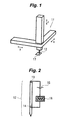
- FIG. 1 there is schematically illustrated the CDW quantum phase microscope as the first embodiment of the present invention.
- the CDW quantum phase microscope includes a piezoelectric controller 11 similar to that adopted in ordinary scanning probe microscopes, and a CDW needle-like crystal-made probe 12 so installed under the piezoelectric controller 11 that it can be scanned three-dimensionally in the x-, y- and z-directions by the piezoelectric controller 11.
- the probe 12 includes electrodes 13 and 14 between which there is connected an external circuit including a power source 15 and frequency meter 16.
- the frequency of NBS can be measured by the frequency meter 16 to measure a change in threshold electric field.
- the above CDW quantum phase microscope is to be used as will be discussed below. It should be noted here that the microscope is used to inspect a specimen made of a CDW nano-structure as an example.
- the probe 12 is scanned while being kept in contact with the surface of a specimen 17 made of the CDW nano-structure as shown in FIG. 1.
- the tip of the probe 12 is displaced, which causes a stress in the probe 12.
- the stress will cause the threshold electric field of the probe 12 to change, and the change in threshold electric field will cause the frequency of NBS flowing through the probe 12 to change.
- the change of the NBS frequency is converted into a surface image.
- the conversion into a surface image in other words, visualization of a surface shape of an object, may be made through visualization of the output of a frequency-voltage (current) converter or visualization of a control signal providing a feedback.
- the CDW quantum phase microscope may be used in another way as will be described below:
- the CDW quantum phase microscope may be used in still another way as will be described below. It should be noted that the CDW tunneling is utilized in this use of the CDW quantum phase microscope.
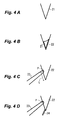
- the probe 12 is scanned over the surface of the specimen 17 made of the CDW nano-structure while being brought closer to the surface. It is assumed here that the phase of CDW at the tip of the probe 12 is ⁇ p and the phase of CDW on the surface of the specimen 17 is ⁇ s . When the tip of the probe 12 is displaced as it is scanned, ⁇ s will correspondingly change, resulting in a change of ⁇ p - ⁇ s , so that the tunneling current flowing between the probe 12 and specimen 17 will change. A change of this current or voltage is converted into a surface image.
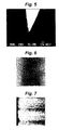
- the probe 12 made of a CDW needle-like crystal is produced as will be described below:
- the Ta film was 100 nm in thickness and Se film was 200 nm in thickness.
- the spot size of the electron beam 23 was 1 ⁇ m, acceleration voltage was 25 kV, irradiation current amount was 1 ⁇ 10 -7 ⁇ A and irradiation time was 30 min. Also, the electron beam 23 was irradiated in a vacuum of 3 to 4 ⁇ 10 -6 Torr.
- FIG. 5 is a scanning electron microscope (SEM) micrograph of the needle-like crystal.
- SEM scanning electron microscope
- FIG. 6 is a micrograph showing an excellent atomic image obtained.
- FIG. 7 is a micrograph of a CDW image obtained by the CDW quantum phase microscope.
- a CDW quantum phase microscope which actively utilizes macroscopic quantum phase information on CDW.
- the CDW quantum phase microscope is a high-precision one higher in functionality than AFM. For example, use of a 100 nm-long CDW probe 12 permits to implement a microscope having a resolution of 1 pm with the sensitivity of a frequency meter 16 used being 1 Hz. Also, since this CDW quantum phase microscope needs not any optical system used in AFM or the like, it can advantageously be designed correspondingly smaller.
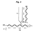
- the CDW quantum phase microscope uses a probe 32 made of Si or the like and installed below one end of a cantilever 31 as shown in FIG. 8. The other end of the cantilever 31 is installed to a piezoelectric controller (not shown).
- a CDW needle-like crystal 33 is provided integrally on the cantilever 31. Electrodes 34 and 35 are provided at both ends, respectively, of the CWD needle-like crystal 33, and an external circuit including a power source 36 and frequency meter 37 is connected between the electrodes 34 and 35.
- the frequency meter 37 can be used to measure the frequency of NBS, and a change in threshold electric field of the CDW needle-like crystal 33 be measured based on the measured NBS frequency.
- the above CDW quantum phase microscope is to be used as will be discussed below. It should be noted here that the microscope is used to inspect a specimen made of a CDW nano-structure as an example.
- the probe 32 is scanned over the surface of a specimen 17 made of the CDW nano-structure while being kept in contact with the specimen surface as shown in FIG. 8.
- the tip of the probe 32 is displaced and the one end of the cantilever 31 is thus displaced, which causes the CDW needle-like crystal 33 on the cantilever 31 to expand and contract, which will cause a stress to develop in the CDW needle-like crystal 33.
- the stress will cause the threshold electric field of the CDW needle-like crystal 33 to change, which will cause the frequency of NBS flowing through the CDW needle-like crystal 33 to change. And the change of the NBS frequency is converted into a surface image.
- the above second embodiment is similar to the aforementioned first embodiment except for respects other than the above-mentioned ones.
- the second embodiment has similar advantages to those of the first embodiment.
- FIG. 9 schematically illustrates the CDW quantum interferometer.
- the CDW quantum interferometer includes a CDW needle-like crystal 41, electrodes 42 and 43 provided at both ends, respectively, of the CDW needle-like crystal 41 and an external circuit composed of a power source 44 and frequency meter 45 and connected between the electrodes 42 and 43 as shown in FIG. 9.
- a gate electrode 46 On the central side surface of the CDW needle-like crystal 41, there is provided a gate electrode 46 which can apply a gate voltage to the CDW needle-like crystal 41.
- the frequency meter 45 can be used to measure the frequency of NBS, and a change in threshold electric field of the needle-like crystal 41 be measured based on the measured NBS frequency.
- the CDW quantum interferometer is to be used as will be discussed below:
- a CDW quantum interferometer which actively utilizes macroscopic quantum phase information on CDW.
- the CDW quantum interferometer can measure the local electric field with a high precision.
- the magnetic probe microscope uses a ferromagnetic material-made probe 12 prepared like the first embodiment. More particularly, for example, a Ni film is formed on the surface of the cone 21 and an electron beam 23 is irradiated to the Ni film as in the first embodiment to grow a needle-like crystal of Ni. This needle-like crystal is used to form the probe 12.
- the above fourth embodiment is similar to the aforementioned first embodiment except for respects other than the above-mentioned ones.
- a magnetic probe microscope using an exellent probe 12 formed from a ferromagnetic material.
- This magnetic material probe microscope can be used to inspect a ferromagnetic material with a high precision.
- the diamagnetic probe microscope uses a diamagnetic material-made probe 12 prepared like the first embodiment. More particularly, for example, a Cu film is formed on the surface of the cone 21 and an electron beam 23 is irradiated to the Cu film as in the first embodiment to grow a needle-like crystal of Cu. This needle-like crystal is used to form the probe 12.
- the above fifth embodiment is similar to the aforementioned first embodiment except for respects other than the above-mentioned ones.
- the fifth embodiment it is possible to implement a diamagnetic probe microscope using an excellent probe 12 formed from a diamagnetic material.
- This diamagnetic probe microscope can be used to inspect a diamagnetic material with a high precision.
- the multi-probe CDW quantum phase microscope uses a probe 53 prepared by forming multiple cones 52 in a two-dimensional array on a substrate 51 and growing a CDW needle-like crystal on the tip of each cone 52 in the similar manner to that adopted to make the probe as the first embodiment.
- the above sixth embodiment is similar to the aforementioned first embodiment except for respects other than the above-mentioned ones.
- the multi-probe CDW quantumphase microscope according to the sixth embodiment can be used to inspect a wide range of a CDW specimen with a high precision.
- multiple blade-shaped portions 62 are formed like stripes in parallel with each other on a substrate 61 and probes 63 are formed in a one-dimensional array on the tip of each blade-shaped portion 62 as shown in FIG. 11.
- the general view of the plurality of blade-shaped portions 62 is such that the probes 63 are disposed in a two-dimensional array.
- Each of the probes 63 is formed by irradiating an electron beam 23 to a point on the substrate 61 apart from the tip of the blade-shaped portion 62 as in the first embodiment.
- the above seventh embodiment is similar to the aforementioned first embodiment except for respects other than the above-mentioned ones.
- the multi-probe CDW quantum phase microscope as the seventh embodiment can be used to inspect a wide range of a CDW specimen collectively and with a high precision.
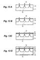
- multiple cones 72 are formed in a two-dimensional array on a n-type GaAs substrate 71, for example, and a needle-like semiconductor crystal 73 of n-type GaAs, for example, is formed on the tip of each of the cones 72 in the similar manner to that adopted to produce the first embodiment, as shown in FIG. 12.
- a Schottky electrode material is formed to bury around the needle-like semiconductor crystal 73 on the insulating film 74 to form a gate electrode 75 as shown in FIG. 13B.
- an ohmic electrode material is formed on the insulating layer 76 to form a drain electrode 77 which is in ohmic contact with the upper end of the needle-like semiconductor crystal 73 as shown in FIG. 13D.
- the ohmic electrode material is formed on the rear side of the n-type GaAs substrate 71 to form a source electrode 78.
- an integrated FET in which micro Schottky gate FETs formed from the needle-like semiconductor crystal 73 are disposed in a two-dimensional array can easilybe produced without use of lithography except in the process of forming the cones 72.
- the gate electrodes 75 and drain electrodes 77 are patterned on each FET as shown in FIG. 14.
- the gate electrodes 75 are connected to each other by predetermined wiring (not shown) and also the drain electrodes 77 are connected to each other by predetermined wiring (not shown) .
- FETs can be driven independently of each other.
- the two-dimensional quantum dot array can easily be produced.
- the eleventh embodiment of the present invention will be explained.
- the probe 12 made of the CDW needle-like crystal is produced in a manner different from that adopted to produce the first embodiment.
- a CDW crystal substrate 91 is first prepared and its surface is irradiated to a predetermined point thereon with an electron beam 23 at room temperature as shown in FIG. 16A.
- the spot size of the electron beam 23 may be about 50 nm to 1 ⁇ m, for example.
- the CDW crystal substrate 91 is heated to a temperature nearly equal to its melting point at the point irradiated with the electron beam 23.
- the CDW crystal substrate 91 thus melted is recrystallized to grow the CDW needle-like crystal 24 as shown in FIG. 16B.
- the CDW needle-like crystal 24 may be, for example, about 5 nm to 1 ⁇ m in thickness (diameter), 10 nm to 2 ⁇ m in length or 10 to 500 nm, and 100 or less in aspect ratio (length/thickness) as a rule.
- the electron beam 23 was irradiated to the predetermined point on the surface of the CDW crystal substrate 91 formed from the TaSe 2 crystal.
- the CDW crystal substrate 91 has a square shape of which each side is about 40 ⁇ m long.
- the electron beam 23 was irradiated to a spot of 1 ⁇ m in size with an irradiation current of 8 ⁇ 10 -8 A at an acceleration voltage of 25 kV for 30 min. Also, the electron beam 23 was irradiated in a vacuum of 3 to 4 ⁇ 10 -6 Torr.
- the CDW needle-like crystal 24 made of the single crystal TaSe 2 needle-like crystal (nano-fiber) of about 50 nm in diameter was grown to a length of about 150 nm contiguously with the CDW crystal substrate 91 on the CDW crystal substrate 91 made of the TaSe 2 crystal.
- the CDW needle-like crystal 24 suitable for use in a CDW quantum phase microscope can be provided.
- FIG. 18 is a phase diagram of La 2-x Ba x CuO 4 .
- the spin/charge stripe order is stabilized at a lower temperature so that the system becomes insulative and the superconductivity is inhibited.
- the spin/charge stripe order will be inhibited and the superconductivity be recovered as shown in FIG. 19.
- the pressure coefficient of T c , dT c /dP will be -3K/kbar, which is 2 or 3 orders of magnitude higher than that of the conventional superconductor.
- a weight of about 0.1 ⁇ gw to the LBCO probe 112 having a tip of several nanometers in diameter permits to implement the probe tip superconductive.
- the tip of the LBCO probe 112 having a superconductivity susceptible to such a pressure into contact with the surface of the specimen 113 so as to apply the tip of the LBCO probe 112 with a pressure higher than the pressure under which the superconductivity is recovered, the tip of the LBCO probe 112 having been insulative becomes superconductive so that the I-V characteristic between the LBCO probe 112 and specimen 113 will be changed due to the Andreev reflection.
- the LBCO probe 112 should be cooled to a temperature lower than the superconducting critical temperature when the pressure is applied and to a temperature higher than the superconducting critical temperature when no pressure is applied.
- the above I-V characteristic change can be utilized to make the following measurement, for example:
- the LBCO probe 112 is produced as will be discussed below:
Landscapes
- Chemical & Material Sciences (AREA)
- Health & Medical Sciences (AREA)
- General Health & Medical Sciences (AREA)
- Engineering & Computer Science (AREA)
- Nuclear Medicine, Radiotherapy & Molecular Imaging (AREA)
- Radiology & Medical Imaging (AREA)
- General Physics & Mathematics (AREA)
- Physics & Mathematics (AREA)
- Nanotechnology (AREA)
- Crystallography & Structural Chemistry (AREA)
- Life Sciences & Earth Sciences (AREA)
- Molecular Biology (AREA)
- Analytical Chemistry (AREA)
- Crystals, And After-Treatments Of Crystals (AREA)
- Testing Or Measuring Of Semiconductors Or The Like (AREA)
Applications Claiming Priority (4)
| Application Number | Priority Date | Filing Date | Title |
|---|---|---|---|
| JP2004128772A JP4413066B2 (ja) | 2004-04-23 | 2004-04-23 | 電荷密度波量子位相顕微鏡及び電荷密度波量子干渉計 |
| JP2004128770A JP2005308651A (ja) | 2004-04-23 | 2004-04-23 | 走査プローブ顕微鏡およびその使用方法 |
| JP2004128771A JP2005308652A (ja) | 2004-04-23 | 2004-04-23 | プローブ顕微鏡探針及びその製造方法並びにプローブ顕微鏡並びに針状体及びその製造方法並びに電子素子及びその製造方法 |
| PCT/JP2005/008259 WO2005103646A1 (ja) | 2004-04-23 | 2005-04-22 | 走査プローブ顕微鏡探針及びその製造方法並びに走査プローブ顕微鏡及びその使用方法並びに針状体及びその製造方法並びに電子素子及びその製造方法並びに電荷密度波量子位相顕微鏡並びに電荷密度波量子干渉計 |
Publications (1)
| Publication Number | Publication Date |
|---|---|
| EP1744143A1 true EP1744143A1 (de) | 2007-01-17 |
Family
ID=35197087
Family Applications (1)
| Application Number | Title | Priority Date | Filing Date |
|---|---|---|---|
| EP05736881A Withdrawn EP1744143A1 (de) | 2004-04-23 | 2005-04-22 | Rastersondenmikroskopsonde und herstellungsverfahren dafür sowie rastersondenmikroskop und anwendungsverfahren dafür sowie nadelähnliches element und herstellungsverfahren dafür sowie elektronenelement und herstellungsverfahren dafür sowie ladungsdichtewellenquantum-phasenmikroskop und ladungsdichtewellenquantum-interferometer |
Country Status (4)
| Country | Link |
|---|---|
| US (1) | US7553335B2 (de) |
| EP (1) | EP1744143A1 (de) |
| KR (1) | KR20070012803A (de) |
| WO (1) | WO2005103646A1 (de) |
Families Citing this family (7)
| Publication number | Priority date | Publication date | Assignee | Title |
|---|---|---|---|---|
| KR20080006590A (ko) * | 2005-04-07 | 2008-01-16 | 이 창 훈 | 프로브, 프로브의 제조방법 및 프로브의 응용 |
| KR100761059B1 (ko) | 2006-09-29 | 2007-09-21 | 파크시스템스 주식회사 | 오버행 샘플 측정이 가능한 주사 탐침 현미경 |
| US7635392B2 (en) * | 2007-08-14 | 2009-12-22 | Qimonda Ag | Scanning probe microscopy cantilever, corresponding manufacturing method, scanning probe microscope, and scanning method |
| US10481174B2 (en) * | 2015-03-11 | 2019-11-19 | Yeda Research And Development Co. Ltd. | Superconducting scanning sensor for nanometer scale temperature imaging |
| CN105572423B (zh) * | 2016-01-22 | 2018-06-26 | 复旦大学 | 一种基于无液氦室温孔超导磁体的强磁场扫描探针显微镜 |
| CN112960644A (zh) * | 2021-02-03 | 2021-06-15 | 中国科学院长春光学精密机械与物理研究所 | 基于针尖增强的电子束诱导碳基纳米结构的可控生长方法 |
| KR102512651B1 (ko) | 2021-03-25 | 2023-03-23 | 연세대학교 산학협력단 | 주사탐침 현미경용 프로브 및 이를 포함하는 이진 상태 주사탐침 현미경 |
Family Cites Families (5)
| Publication number | Priority date | Publication date | Assignee | Title |
|---|---|---|---|---|
| US3717814A (en) * | 1971-09-23 | 1973-02-20 | Bell Telephone Labor Inc | Cophasing diversity communication system with pilot feedback |
| JPH081382B2 (ja) | 1990-10-31 | 1996-01-10 | インターナショナル・ビジネス・マシーンズ・コーポレイション | ナノメートル・スケールのプローブ及びその製造方法 |
| JP2002181682A (ja) | 2000-12-14 | 2002-06-26 | Jeol Ltd | 電子対測定装置および走査形トンネル顕微鏡 |
| JP2002255699A (ja) * | 2001-02-26 | 2002-09-11 | Komatsu Ltd | 環状結晶体及びその製造方法 |
| JP4688400B2 (ja) * | 2001-12-04 | 2011-05-25 | エスアイアイ・ナノテクノロジー株式会社 | 走査型プローブ顕微鏡用探針 |
-
2005
- 2005-04-22 US US11/568,223 patent/US7553335B2/en not_active Expired - Fee Related
- 2005-04-22 EP EP05736881A patent/EP1744143A1/de not_active Withdrawn
- 2005-04-22 KR KR1020067020386A patent/KR20070012803A/ko not_active Withdrawn
- 2005-04-22 WO PCT/JP2005/008259 patent/WO2005103646A1/ja not_active Ceased
Non-Patent Citations (1)
| Title |
|---|
| See references of WO2005103646A1 * |
Also Published As
| Publication number | Publication date |
|---|---|
| US7553335B2 (en) | 2009-06-30 |
| WO2005103646A1 (ja) | 2005-11-03 |
| KR20070012803A (ko) | 2007-01-29 |
| US20070272855A1 (en) | 2007-11-29 |
Similar Documents
| Publication | Publication Date | Title |
|---|---|---|
| US10903411B2 (en) | Semiconductor Josephson junction and a transmon qubit related thereto | |
| Zeljkovic et al. | Interplay of chemical disorder and electronic inhomogeneity in unconventional superconductors | |
| Xiang et al. | Quantum melting of a disordered Wigner solid | |
| US7553335B2 (en) | Scanning probe microscope probe and manufacturing method therefor, scanning probe microscope and using method therefor, needle-like body and manufacturing method therefor, electronic device and manufacturing method therefor, charge density wave quantum phase microscope, and charge density wave quantum interferometer | |
| Calahorra et al. | Exploring piezoelectric properties of III–V nanowires using piezo-response force microscopy | |
| Sachin et al. | Altermagnetic Superconducting Diode Effect in Mn $ _ {3} $ Pt/Nb Heterostructures | |
| Seredinski et al. | Supercurrent in graphene Josephson junctions with narrow trenches in the quantum Hall regime | |
| US20240389476A1 (en) | High temperature superconducting devices and methods thereof | |
| JP4413066B2 (ja) | 電荷密度波量子位相顕微鏡及び電荷密度波量子干渉計 | |
| Guo | Reconfigurable graphene complex oxide nanostructures | |
| Wright | Growth and applications of epitaxial transition metal nitride thin film heterostructures | |
| JP2005308652A (ja) | プローブ顕微鏡探針及びその製造方法並びにプローブ顕微鏡並びに針状体及びその製造方法並びに電子素子及びその製造方法 | |
| Ariskina | Local magnetic identification and characterization of superconducting graphite interfaces at room temperature | |
| Werder et al. | Anodic Oxidation Nanolithography with Atomic Force Microscope | |
| Yildiz et al. | Local probing of superconductivity at oxide interfaces with atomic force microscopy | |
| Zhang | Nanoscale Characterization and Engineering of Topological and Magnetic Materials | |
| Susła et al. | Scanning tunneling microscopy/spectroscopy of ferromagnetic Ni clusters on graphite and BSCCO high-Tc superconductor | |
| Collomb | Development of graphene-based sensors for scanning Hall microscopy and imaging of vortex matter in unconventional superconductors | |
| Yang | Nonlinear transport in noncentrosymmetric materials | |
| Li | Josephson Junctions and SQUIDs Based on CVD Graphene | |
| Tang | Electronic Properties in Nanowire-based Complex Oxide Devices | |
| Zhang | The Growth of Large-Scale Single-Crystal Monolayer Transition Metal Disulfide Materials in High-Vacuum System Based on Passivated Semiconductor | |
| Park | Lateral and Vertical Electronic Transport Properties of Topological Insulator-Based Van Der Waals Heterostructures Grown by Molecular Beam Epitaxy | |
| Somnath | Monday Morning, November 7, 2016 | |
| Hasegawa et al. | Scanning Tunnelling Spectroscopy of Layered Cuprates and Transition Metal Chalcogenides |
Legal Events
| Date | Code | Title | Description |
|---|---|---|---|
| PUAI | Public reference made under article 153(3) epc to a published international application that has entered the european phase |
Free format text: ORIGINAL CODE: 0009012 |
|
| 17P | Request for examination filed |
Effective date: 20061123 |
|
| AK | Designated contracting states |
Kind code of ref document: A1 Designated state(s): DE FI NL |
|
| AX | Request for extension of the european patent |
Extension state: AL BA HR LV MK YU |
|
| RIN1 | Information on inventor provided before grant (corrected) |
Inventor name: IDO, MASAYUKI Inventor name: NISHIDA, MUNEHIROGRAD.SCHOOL OF ENG.,HOKKAIDO UNI Inventor name: MOMONO, NAOKI Inventor name: TAKESHI TOSHIMA Inventor name: OHKAWA, HIROYUKI Inventor name: INAGAKI, KATSUHIKO Inventor name: ODA, MIGAKU Inventor name: TANDA, SATOSHI |
|
| RIN1 | Information on inventor provided before grant (corrected) |
Inventor name: IDO, MASAYUKI Inventor name: NISHIDA, MUNEHIROGRAD.SCHOOL OF ADV.SCIENCES OF MA Inventor name: MOMONO, NAOKI Inventor name: TAKESHI TOSHIMA Inventor name: OHKAWA, HIROYUKI Inventor name: INAGAKI, KATSUHIKO Inventor name: ODA, MIGAKU Inventor name: TANDA, SATOSHI |
|
| RBV | Designated contracting states (corrected) |
Designated state(s): DE FI NL |
|
| STAA | Information on the status of an ep patent application or granted ep patent |
Free format text: STATUS: THE APPLICATION HAS BEEN WITHDRAWN |
|
| 18W | Application withdrawn |
Effective date: 20080505 |