EP1744400A2 - Système d'antenne à large bande - Google Patents
Système d'antenne à large bande Download PDFInfo
- Publication number
- EP1744400A2 EP1744400A2 EP06114894A EP06114894A EP1744400A2 EP 1744400 A2 EP1744400 A2 EP 1744400A2 EP 06114894 A EP06114894 A EP 06114894A EP 06114894 A EP06114894 A EP 06114894A EP 1744400 A2 EP1744400 A2 EP 1744400A2
- Authority
- EP
- European Patent Office
- Prior art keywords
- antenna system
- conductor
- broadband antenna
- feed
- ground plane
- Prior art date
- Legal status (The legal status is an assumption and is not a legal conclusion. Google has not performed a legal analysis and makes no representation as to the accuracy of the status listed.)
- Granted
Links
Images


Classifications
-
- H—ELECTRICITY
- H01—ELECTRIC ELEMENTS
- H01Q—ANTENNAS, i.e. RADIO AERIALS
- H01Q1/00—Details of, or arrangements associated with, antennas
- H01Q1/12—Supports; Mounting means
- H01Q1/22—Supports; Mounting means by structural association with other equipment or articles
- H01Q1/2291—Supports; Mounting means by structural association with other equipment or articles used in Bluetooth® or Wi-Fi® devices of Wireless Local Area Networks [WLAN]
-
- H—ELECTRICITY
- H01—ELECTRIC ELEMENTS
- H01Q—ANTENNAS, i.e. RADIO AERIALS
- H01Q5/00—Arrangements for simultaneous operation of antennas on two or more different wavebands, e.g. dual-band or multi-band arrangements
- H01Q5/50—Feeding or matching arrangements for broad-band or multi-band operation
-
- H—ELECTRICITY
- H01—ELECTRIC ELEMENTS
- H01Q—ANTENNAS, i.e. RADIO AERIALS
- H01Q9/00—Electrically-short antennas having dimensions not more than twice the operating wavelength and consisting of conductive active radiating elements
- H01Q9/04—Resonant antennas
- H01Q9/16—Resonant antennas with feed intermediate between the extremities of the antenna, e.g. centre-fed dipole
- H01Q9/26—Resonant antennas with feed intermediate between the extremities of the antenna, e.g. centre-fed dipole with folded element or elements, the folded parts being spaced apart a small fraction of operating wavelength
-
- H—ELECTRICITY
- H01—ELECTRIC ELEMENTS
- H01Q—ANTENNAS, i.e. RADIO AERIALS
- H01Q9/00—Electrically-short antennas having dimensions not more than twice the operating wavelength and consisting of conductive active radiating elements
- H01Q9/04—Resonant antennas
- H01Q9/30—Resonant antennas with feed to end of elongated active element, e.g. unipole
- H01Q9/32—Vertical arrangement of element
- H01Q9/36—Vertical arrangement of element with top loading
Definitions
- the present invention is directed to broadband antennas. More particularly, the present invention relates to a small-sized broadband antenna system having an integrated matching circuit.
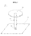
- FIG 1 illustrates a structure of a conventional quarter-wavelength monopole antenna system.
- an antenna system 100 consists of an antenna positioned perpendicularly to a ground plane 110.
- a radiation pattern is formed between the antenna 120 and the ground plane 110 by connecting a lower end of the antenna 120 to a power source 130 that supplies signals.
- An upper end of the antenna 120 may be terminated by a metal plate 140, which acts as a capacitance load against the ground plane 110 in order to shorten the height of the antenna 120.
- the height of the antenna 120 may be shortened by the metal plate 140, but this is not sufficient to meet the need for wireless products to be small and compact.
- the present invention provides a broadband antenna system capable of reducing the size of an antenna system and obtaining a broad bandwidth, without adversely affecting the antenna gain and radiation characteristics.
- a broadband antenna system comprising a ground plane, a metal plate parallel to the ground plane, and constituting a capacitance load against the ground plane, and a radiation structure connected perpendicularly to the ground plane and the metal plate, wherein the radiation structure includes a feed conductor to supply an electric signal, a short-circuit stub to transfer the supplied electric signal to the ground plane, a first plane comprising a conducting bridge to interconnect the feed conductor and the short-circuit stub, which is separated from the metal plate, and a second plane comprising a radiating conductor connected to the ground plane the metal plate, and coupled to a supplied signal to thereby radiate electromagnetic waves.
- a broadband antenna system comprising a ground plane, a metal plate parallel to the ground plane, and constituting a capacitance load against the ground plane, a radiation structure to interconnect the ground plane and the metal plate, wherein the radiation structure includes a feed conductor to supply an electric signal, a short circuit stub to transfer the supplied electric signal to the ground plane, a connecting bridge to interconnect the feed conductor and the short-circuit stub, which is separated from the metal plate, and a radiating conductor connected perpendicularly to the metal plate and the ground plane and coupled to the supplied electric signal, to thereby radiate electromagnetic waves.
- a broadband antenna system comprising a pair of feed wires, a pair of metal plates parallel to oppositely faced feed wires, and between which the feed wires are positioned, and a radiation structure to interconnect the feed wires and the metal plates, wherein the radiation structure includes a feed conductor separated from the metal plates, into which an electric signal is input through the feed wires on one side thereof, and a radiating conductor connected perpendicularly to the metal plate on the other side thereof and coupled to the electric signal to thereby radiate electromagnetic waves.
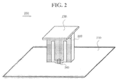
- FIG. 2 illustrates a construction of a broadband antenna system according to an exemplary embodiment of the present invention.
- the broadband antenna system 200 comprises a ground plane 210, a metal plate 230, a radiation structure 220, and a power source 240.
- the power source 240 supplies signals to be transferred to the radiation structure 220.
- the radiation structure 220 may be shaped like a rectangular parallelepiped.
- a conductor along which signals are transferred may be formed on the surfaces of opposite planes of the radiation structure 220. Further, opposite ends of the radiation structure 220 are connected perpendicularly to the ground plane 210 and the metal plate 230 respectively.
- the metal plate 230 is parallel to the ground plane 210, and acts as a capacitance load against the ground plane 210. Accordingly, since the broadband antenna system 200 may be represented as an equivalent circuit having a transmission conductor line that is shorter than a quarter-wavelength, the size of the broadband antenna system 200 may be reduced.
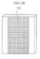
- Figures 3A and 3B a construction of the plane on which the conductor is formed is illustrated in Figures 3A and 3B.
- Figure 3A shows a front view of the radiation structure 220
- Figure 3B shows a rear view of the radiation structure 220.
- a feed conductor 220a, a short-circuit stub 220b, and a conducting bridge 220c are formed on the front side of the radiation structure 220.
- a radiation conductor 220d is formed on the rear side thereof.
- One end of the short-circuit stub 220b is connected to the ground plane 210 shown in Figure 2, and the other end is connected to the conducting bridge 220c.
- the conducting bridge 220c is separated from the metal plate 230 shown in Figure 2, and one end of the radiating conductor 220d is connected to the ground plane 210, and the other end is connected to the metal plate 230.
- electromagnetic waves are generated in the radiating conductor 220d as the input signal is coupled to the radiating conductor 220d, whereby the input signal is transmitted into a free space.
- the signal fed to the feed conductor 220a is transmitted to the short-circuit stub 220b through the conducting bridge 220c, and is then transmitted to the ground plane 210.
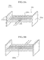
- FIGS. 4A and 4B illustrate a construction of a broadband antenna system according to another exemplary embodiment of the present invention.
- the broadband antenna system 400 illustrated in Figure 4A comprises a ground plane 410, a radiation structure 420 and a metal plate 430, which is similar in shape to the broadband antenna system depicted in Figure 2.
- the broadband antenna system 400 depicted in Figure 4A is constructed with three planes or layers (i.e., a front layer, a middle layer and a rear layer), on which the conductors are disposed.
- the broadband antenna system 200 of Figure 2 has two planes, on which the conductors are disposed, i.e., a first plane into which an electric signal is input, and a second plane from which electromagnetic waves radiate.
- a first plane into which an electric signal is input i.e., a first plane into which an electric signal is input
- a second plane from which electromagnetic waves radiate i.e., a second plane from which electromagnetic waves radiate.
- an electric signal is input into the middle layer, and electromagnetic waves radiate from both the front layer and the rear layer.
- the radiation structure 420 includes two rectangular parallelepipeds 422 and 424 which are constructed as shown in Figures 3A and 3B.
- the rectangular parallelepipeds 422 and 424 are oppositely coupled so that conductors, into which signals are input from the power source 440, are disposed on opposite faces of the middle layer, and radiating conductors are disposed on the other faces, i.e., the front layer and the rear layer.
- Figures 5A and 5B also illustrate a construction of a broadband antenna system according to another exemplary embodiment of the present invention.
- the broadband antenna system 500 depicted in Figure 5A comprises a ground plane 510, a metal plate 530 parallel to the ground plane 510 and acting as a capacitance load against the ground plane 510, and a radiation structure 520 to interconnect the ground plane 510 and the metal plate 530.
- the radiation structure 520 comprises a feed conductor 540 to provide an electric signal, two short-circuit stubs 520a and 520b to transfer the provided electric signal to the ground plane 510, a conducting bridge 522 to interconnect the feed conductor 540 and the short-circuit stubs 520a and 520b, which is separated from the metal plate 530, and two radiating conductors 520c and 520d connected perpendicularly to the metal plate 530 and the ground plane 510, and coupled to the provided electric signal to thereby radiate electromagnetic waves.
- the broadband antenna system 500 of Figure 5A comprises two short-circuit stubs 520a and 520b, and two radiating conductors 520c and 520d.
- Figure 5B is a top plan view of the radiation structure 520, which corresponds to a planar structure of a coaxial cable.
- An internal conductor of the coaxial cable, to which a signal is transferred, corresponds to the feed conductor 540, and an external conductor thereof corresponds to two short-circuit stubs 520a and 520b, and two radiating conductors 520c and 520d.
- the short-circuit stubs 520a and 520b can be distinguished from the radiating conductors 520c and 520d by truncating a part of the external conductor of the coaxial cable. The truncated part is indicated by the reference numeral 544 in Figure 5B.
- the two short-circuit stubs 520a and 520b, and the two radiating conductors 520c and 520d are opposite one another, relative to the feed conductor 540.
- Figure 5C shows the structure of the radiation structure 520 when viewed in the "A" direction of Figure 5A
- Figure 5D shows the structure of the radiation structure 520 when viewed in the "B" direction of Figure 5A.
- Figure 6 illustrates a broadband antenna system 600 similar in shape to the broadband antenna system 500 depicted in Figure 5A.
- the broadband antenna system 600 comprises a ground plane 610, a metal plate 630 parallel to the ground plane 610 and acting as a capacitance load against the ground plane 610, and a radiation structure 620 to interconnect the ground plane 610 and the metal plate 630.
- the radiation structure 620 comprises a feed conductor 640 to provide an electric signal, short-circuit stubs 620a and 620b to transfer the provided electric signal to the ground plane 610, a conducting bridge 622 to interconnect the feed conductor 640 and the short-circuit stubs 620a and 620b, which is separated from the metal plate 630, and radiating conductors 620c and 620d connected perpendicularly to the metal plate 630 and the ground plane 610, and coupled to the provided electric signal to thereby radiate electromagnetic waves.
- the broadband antenna system 600 of Figure 6 comprises two short-circuit stubs 620a and 620b, and two radiating conductors 620c and 620d, which are opposite one another, relative to the feed conductor 640.
- the feed conductor 640, the short-circuit stubs 620a and 620b, and the radiating conductors 620c and 620d may be formed of wire conductors.
- FIGS 7A and 7B illustrate a construction of a broadband antenna system according to a still further exemplary embodiment of the present invention.
- the broadband antenna system 700 comprises a pair of feed wires 740, metal plates 730a and 730b parallel to the feed wires 740 (oppositely faced), and between which the feed wires 740 are disposed, and a radiation structure 720 to interconnect the feed wires 740 and the metal plates 730a and 730a.
- the feed conductor 720a On one side of the radiation structure 720 is formed the feed conductor 720a which can receive an input electric signal transmitted from the feed wire 740 since stubs are formed thereon. Since the feed wires 740 have positive (+) and negative (-) poles, the broadband antenna system 700 depicted in Figure 7A can operate as a dipole antenna. Further, the feed conductor 720a is separated from the metal plates 730a and 730b.
- a radiating conductor 720b connected perpendicularly to the metal plates 730a and 730b and coupled to the provided electric signal, to thereby generate electromagnetic waves.
- the feed wires 740 are connected perpendicularly to the feed conductor 720a.
- FIGs 8A and 8B illustrate a construction of a broadband antenna system according to a still further exemplary embodiment of the present invention, which is similar to that of the broadband antenna system depicted in Figures 7A and 7B.
- This broadband antenna system 800 comprises a pair of feed wires 840, metal plates 830a and 830b which are parallel to the feed wires 840 and which are oppositely faced and between which the feed wires 840 are disposed, and a radiation structure 820 to interconnect the feed wire 840 and the metal plates 830a and 830b.
- the feed conductor 820a On one side of the radiation structure 820 is formed the feed conductor 820a which can receive an input electric signal transmitted from the feed wire 840 since stubs are formed thereon.
- the feed wires 840 have positive (+) and negative (-) poles
- the broadband antenna system 800 depicted in Figure 8A can operate as a dipole antenna.
- the feed conductor 820a is separated from the metal plates 830a and 830b.
- a radiating conductor 820b connected perpendicularly to the metal plates 830a and 830b, and coupled to the supplied signal to thereby generate electromagnetic waves.
- the feed wires 840 and the feed conductor 820a are formed so as to be interconnected on the same plane.
- VSWR voltage standing wave ratio
- Figure 10 illustrates measurement results obtained from the AgilentTM network analyzer when a prototype of a broadband antenna system according to the present invention is measured. Referring to this, when an S11 parameter is 2, a bandwidth in the range of about 4.8 GHz to about 6.9 GHz is obtained.
- the broadband antenna system according to the present invention can be applied to a broadband wireless local area network (WLAN), a multi input multi output (MIMO) system, and a wireless digital television. Further, a broadband antenna system in an array form can be constructed of several broadband antenna systems.
- WLAN wireless local area network
- MIMO multi input multi output
- a broadband antenna system in an array form can be constructed of several broadband antenna systems.
- a small-sized monopole/dipole broadband antenna system is provided which is applicable to a variety of wireless devices requiring broadband communication functionality and compactness.
Landscapes
- Engineering & Computer Science (AREA)
- Computer Networks & Wireless Communication (AREA)
- Details Of Aerials (AREA)
- Variable-Direction Aerials And Aerial Arrays (AREA)
- Aerials With Secondary Devices (AREA)
- Waveguide Aerials (AREA)
Applications Claiming Priority (1)
| Application Number | Priority Date | Filing Date | Title |
|---|---|---|---|
| KR1020050050516A KR100654458B1 (ko) | 2005-06-13 | 2005-06-13 | 광대역 안테나 시스템 |
Publications (3)
| Publication Number | Publication Date |
|---|---|
| EP1744400A2 true EP1744400A2 (fr) | 2007-01-17 |
| EP1744400A3 EP1744400A3 (fr) | 2007-03-14 |
| EP1744400B1 EP1744400B1 (fr) | 2013-07-31 |
Family
ID=36954937
Family Applications (1)
| Application Number | Title | Priority Date | Filing Date |
|---|---|---|---|
| EP06114894.6A Ceased EP1744400B1 (fr) | 2005-06-13 | 2006-06-02 | Système d'antenne à large bande |
Country Status (4)
| Country | Link |
|---|---|
| US (2) | US7425921B2 (fr) |
| EP (1) | EP1744400B1 (fr) |
| KR (1) | KR100654458B1 (fr) |
| CN (1) | CN1881687B (fr) |
Families Citing this family (13)
| Publication number | Priority date | Publication date | Assignee | Title |
|---|---|---|---|---|
| US7274339B2 (en) * | 2005-09-16 | 2007-09-25 | Smartant Telecom Co., Ltd. | Dual-band multi-mode array antenna |
| US8259021B2 (en) * | 2008-12-22 | 2012-09-04 | Industrial Technology Research Institute | Electromagnetic radiation apparatus and method for forming the same |
| TWI489693B (zh) * | 2011-03-25 | 2015-06-21 | Wistron Corp | 天線模組 |
| KR101339787B1 (ko) | 2012-10-12 | 2013-12-11 | 한국과학기술원 | 안테나 격리도 향상을 위한 구조물 |
| KR20140059552A (ko) * | 2012-11-08 | 2014-05-16 | 삼성전자주식회사 | 수평 방사 안테나 장치 및 이를 구비하는 전자기기 |
| EP2765650A1 (fr) * | 2013-02-08 | 2014-08-13 | Nxp B.V. | Antenne de prothèse auditive |
| US9431712B2 (en) | 2013-05-22 | 2016-08-30 | Wisconsin Alumni Research Foundation | Electrically-small, low-profile, ultra-wideband antenna |
| US9337540B2 (en) | 2014-06-04 | 2016-05-10 | Wisconsin Alumni Research Foundation | Ultra-wideband, low profile antenna |
| CN105048608A (zh) * | 2015-05-26 | 2015-11-11 | 上海大学 | 一种环境电磁波能量收集整流器 |
| CN108933326A (zh) * | 2017-05-24 | 2018-12-04 | 南京濠暻通讯科技有限公司 | 一种螺旋柱面天线 |
| RU2679487C1 (ru) * | 2018-02-26 | 2019-02-11 | Российская Федерация, от имени которой выступает Государственная корпорация по атомной энергии "Росатом" (Госкорпорация "Росатом") | Вибраторная антенна |
| JP7007432B1 (ja) | 2020-07-22 | 2022-01-24 | Dxアンテナ株式会社 | アンテナ装置 |
| CN114696089B (zh) * | 2020-12-28 | 2025-08-15 | 深圳三星通信技术研究有限公司 | 一种辐射天线及其辐射单元 |
Citations (1)
| Publication number | Priority date | Publication date | Assignee | Title |
|---|---|---|---|---|
| US3967276A (en) | 1975-01-09 | 1976-06-29 | Beam Guidance Inc. | Antenna structures having reactance at free end |
Family Cites Families (16)
| Publication number | Priority date | Publication date | Assignee | Title |
|---|---|---|---|---|
| US5181044A (en) * | 1989-11-15 | 1993-01-19 | Matsushita Electric Works, Ltd. | Top loaded antenna |
| JPH08250916A (ja) | 1995-03-07 | 1996-09-27 | Mitsubishi Electric Corp | アンテナ |
| JPH0955620A (ja) | 1995-08-12 | 1997-02-25 | Hironori Nakamura | 無指向性マイクロウェーブ利得アンテナ |
| US6208306B1 (en) * | 1998-04-16 | 2001-03-27 | Emc Automation, Inc. | Compact, broadband antennas based on folded, top-loaded broadband dipoles with high-pass tuning elements |
| DE69914528T2 (de) * | 1998-06-04 | 2004-07-08 | Matsushita Electric Industrial Co., Ltd., Kadoma | Monopolantenne |
| DE60121507T2 (de) * | 2000-05-26 | 2006-12-07 | Matsushita Electric Industrial Co., Ltd., Kadoma | Antenne, Antennenanordnung und Funkgerät |
| ATE448584T1 (de) * | 2001-01-26 | 2009-11-15 | Agency Science Tech & Res | Breitband-aufhängungsplattenantennen mit geringer kreuzpolarisation |
| US6664930B2 (en) | 2001-04-12 | 2003-12-16 | Research In Motion Limited | Multiple-element antenna |
| JP2003188633A (ja) | 2001-12-20 | 2003-07-04 | Mitsumi Electric Co Ltd | 複合アンテナ装置 |
| DE10209977A1 (de) | 2002-03-07 | 2003-10-02 | Kathrein Werke Kg | Antennenanordnung mit einem Flächendipol |
| CN2563761Y (zh) * | 2002-04-18 | 2003-07-30 | 京信通信系统(广州)有限公司 | 宽频带移动通信室内吸顶式全向天线 |
| JP3996451B2 (ja) | 2002-06-19 | 2007-10-24 | 八木アンテナ株式会社 | シリンダダイポールアンテナ |
| US6950066B2 (en) * | 2002-08-22 | 2005-09-27 | Skycross, Inc. | Apparatus and method for forming a monolithic surface-mountable antenna |
| JP2004201278A (ja) * | 2002-12-06 | 2004-07-15 | Sharp Corp | パターンアンテナ |
| JP2004228984A (ja) | 2003-01-23 | 2004-08-12 | Alps Electric Co Ltd | アンテナ装置 |
| US7046199B2 (en) * | 2003-02-13 | 2006-05-16 | Skycross, Inc. | Monolithic low profile omni-directional surface-mount antenna |
-
2005
- 2005-06-13 KR KR1020050050516A patent/KR100654458B1/ko not_active Expired - Fee Related
- 2005-12-29 US US11/319,426 patent/US7425921B2/en not_active Expired - Fee Related
- 2005-12-31 CN CN2005101376573A patent/CN1881687B/zh not_active Expired - Fee Related
-
2006
- 2006-06-02 EP EP06114894.6A patent/EP1744400B1/fr not_active Ceased
-
2008
- 2008-08-05 US US12/186,171 patent/US7764242B2/en not_active Expired - Fee Related
Patent Citations (1)
| Publication number | Priority date | Publication date | Assignee | Title |
|---|---|---|---|---|
| US3967276A (en) | 1975-01-09 | 1976-06-29 | Beam Guidance Inc. | Antenna structures having reactance at free end |
Also Published As
| Publication number | Publication date |
|---|---|
| EP1744400B1 (fr) | 2013-07-31 |
| US7425921B2 (en) | 2008-09-16 |
| EP1744400A3 (fr) | 2007-03-14 |
| CN1881687A (zh) | 2006-12-20 |
| US20060279463A1 (en) | 2006-12-14 |
| KR100654458B1 (ko) | 2006-12-06 |
| CN1881687B (zh) | 2011-05-11 |
| US20090033559A1 (en) | 2009-02-05 |
| US7764242B2 (en) | 2010-07-27 |
Similar Documents
| Publication | Publication Date | Title |
|---|---|---|
| US7764242B2 (en) | Broadband antenna system | |
| AU2007215840B2 (en) | Small-size wide-band antenna and radio communication device | |
| US11095040B2 (en) | Antenna and mimo antenna | |
| KR100836213B1 (ko) | 안테나, 무선장치, 안테나 설계 방법 및 안테나의 동작주파수 측정 방법 | |
| US6603430B1 (en) | Handheld wireless communication devices with antenna having parasitic element | |
| EP1551079A1 (fr) | Antenne à microruban miniaturisée à ultra-large bande | |
| US8786509B2 (en) | Multi polarization conformal channel monopole antenna | |
| US7248224B2 (en) | Antenna device having radiation characteristics suitable for ultrawideband communications | |
| EP2984709B1 (fr) | Antenne réseau et techniques associées | |
| US20100295750A1 (en) | Antenna for diversity applications | |
| CN1318213A (zh) | 电容调谐宽带天线结构 | |
| US20050237244A1 (en) | Compact RF antenna | |
| Tang et al. | A broadband high-efficiency dipole array based on frequency selective surface and integrated feeding structure | |
| WO2000052783A1 (fr) | Antenne a large bande d'un circuit d'adaptation et element radiant sur plaque de masse | |
| JP7407487B1 (ja) | 伝送装置及びアンテナ | |
| US8810332B2 (en) | Electromagnetic coupler and information communication device with same mounted thereon | |
| CN1147967C (zh) | 印刷式偶极天线 | |
| CN116960623A (zh) | 一种天线和电子设备 | |
| TWI451632B (zh) | 高增益迴圈陣列天線系統及電子裝置 | |
| US6297779B1 (en) | Antenna module for portable computer | |
| CN220856921U (zh) | 偶极天线装置 | |
| TWI467853B (zh) | 雙頻天線及應用該雙頻天線之無線通訊裝置 | |
| TWI333716B (en) | Multi-frequency antenna and a related electric device | |
| EP2309592A2 (fr) | Antenne à bande unique | |
| US20060176218A1 (en) | Gain-adjustable antenna |
Legal Events
| Date | Code | Title | Description |
|---|---|---|---|
| PUAI | Public reference made under article 153(3) epc to a published international application that has entered the european phase |
Free format text: ORIGINAL CODE: 0009012 |
|
| AK | Designated contracting states |
Kind code of ref document: A2 Designated state(s): AT BE BG CH CY CZ DE DK EE ES FI FR GB GR HU IE IS IT LI LT LU LV MC NL PL PT RO SE SI SK TR |
|
| AX | Request for extension of the european patent |
Extension state: AL BA HR MK YU |
|
| PUAL | Search report despatched |
Free format text: ORIGINAL CODE: 0009013 |
|
| AK | Designated contracting states |
Kind code of ref document: A3 Designated state(s): AT BE BG CH CY CZ DE DK EE ES FI FR GB GR HU IE IS IT LI LT LU LV MC NL PL PT RO SE SI SK TR |
|
| AX | Request for extension of the european patent |
Extension state: AL BA HR MK YU |
|
| RIC1 | Information provided on ipc code assigned before grant |
Ipc: H01Q 9/36 20060101AFI20061002BHEP Ipc: H01Q 9/26 20060101ALI20070206BHEP Ipc: H01Q 5/00 20060101ALI20070206BHEP |
|
| 17P | Request for examination filed |
Effective date: 20070906 |
|
| 17Q | First examination report despatched |
Effective date: 20071005 |
|
| AKX | Designation fees paid |
Designated state(s): DE FI NL |
|
| RAP1 | Party data changed (applicant data changed or rights of an application transferred) |
Owner name: SAMSUNG ELECTRONICS CO., LTD. |
|
| REG | Reference to a national code |
Ref country code: DE Ref legal event code: R079 Ref document number: 602006037590 Country of ref document: DE Free format text: PREVIOUS MAIN CLASS: H01Q0009360000 Ipc: H01Q0001220000 |
|
| GRAP | Despatch of communication of intention to grant a patent |
Free format text: ORIGINAL CODE: EPIDOSNIGR1 |
|
| RIC1 | Information provided on ipc code assigned before grant |
Ipc: H01Q 1/22 20060101AFI20130109BHEP Ipc: H01Q 9/36 20060101ALI20130109BHEP Ipc: H01Q 9/26 20060101ALI20130109BHEP |
|
| GRAS | Grant fee paid |
Free format text: ORIGINAL CODE: EPIDOSNIGR3 |
|
| GRAA | (expected) grant |
Free format text: ORIGINAL CODE: 0009210 |
|
| AK | Designated contracting states |
Kind code of ref document: B1 Designated state(s): DE FI NL |
|
| REG | Reference to a national code |
Ref country code: DE Ref legal event code: R096 Ref document number: 602006037590 Country of ref document: DE Effective date: 20130926 |
|
| REG | Reference to a national code |
Ref country code: NL Ref legal event code: T3 |
|
| PLBE | No opposition filed within time limit |
Free format text: ORIGINAL CODE: 0009261 |
|
| STAA | Information on the status of an ep patent application or granted ep patent |
Free format text: STATUS: NO OPPOSITION FILED WITHIN TIME LIMIT |
|
| 26N | No opposition filed |
Effective date: 20140502 |
|
| REG | Reference to a national code |
Ref country code: DE Ref legal event code: R097 Ref document number: 602006037590 Country of ref document: DE Effective date: 20140502 |
|
| PGFP | Annual fee paid to national office [announced via postgrant information from national office to epo] |
Ref country code: DE Payment date: 20180522 Year of fee payment: 13 Ref country code: FI Payment date: 20180522 Year of fee payment: 13 |
|
| PGFP | Annual fee paid to national office [announced via postgrant information from national office to epo] |
Ref country code: NL Payment date: 20180523 Year of fee payment: 13 |
|
| REG | Reference to a national code |
Ref country code: DE Ref legal event code: R119 Ref document number: 602006037590 Country of ref document: DE |
|
| REG | Reference to a national code |
Ref country code: FI Ref legal event code: MAE |
|
| PG25 | Lapsed in a contracting state [announced via postgrant information from national office to epo] |
Ref country code: FI Free format text: LAPSE BECAUSE OF NON-PAYMENT OF DUE FEES Effective date: 20190602 |
|
| REG | Reference to a national code |
Ref country code: NL Ref legal event code: MM Effective date: 20190701 |
|
| PG25 | Lapsed in a contracting state [announced via postgrant information from national office to epo] |
Ref country code: NL Free format text: LAPSE BECAUSE OF NON-PAYMENT OF DUE FEES Effective date: 20190701 Ref country code: DE Free format text: LAPSE BECAUSE OF NON-PAYMENT OF DUE FEES Effective date: 20200101 |