EP1744860B1 - Herstellung und verwendung von mikroperforierten substraten - Google Patents
Herstellung und verwendung von mikroperforierten substraten Download PDFInfo
- Publication number
- EP1744860B1 EP1744860B1 EP05716445A EP05716445A EP1744860B1 EP 1744860 B1 EP1744860 B1 EP 1744860B1 EP 05716445 A EP05716445 A EP 05716445A EP 05716445 A EP05716445 A EP 05716445A EP 1744860 B1 EP1744860 B1 EP 1744860B1
- Authority
- EP
- European Patent Office
- Prior art keywords
- substrate
- voltage
- current
- heat
- region
- Prior art date
- Legal status (The legal status is an assumption and is not a legal conclusion. Google has not performed a legal analysis and makes no representation as to the accuracy of the status listed.)
- Expired - Lifetime
Links
Images






Classifications
-
- B—PERFORMING OPERATIONS; TRANSPORTING
- B26—HAND CUTTING TOOLS; CUTTING; SEVERING
- B26D—CUTTING; DETAILS COMMON TO MACHINES FOR PERFORATING, PUNCHING, CUTTING-OUT, STAMPING-OUT OR SEVERING
- B26D7/00—Details of apparatus for cutting, cutting-out, stamping-out, punching, perforating, or severing by means other than cutting
- B26D7/08—Means for treating work or cutting member to facilitate cutting
- B26D7/10—Means for treating work or cutting member to facilitate cutting by heating
-
- B—PERFORMING OPERATIONS; TRANSPORTING
- B26—HAND CUTTING TOOLS; CUTTING; SEVERING
- B26F—PERFORATING; PUNCHING; CUTTING-OUT; STAMPING-OUT; SEVERING BY MEANS OTHER THAN CUTTING
- B26F1/00—Perforating; Punching; Cutting-out; Stamping-out; Apparatus therefor
- B26F1/26—Perforating by non-mechanical means, e.g. by fluid jet
- B26F1/28—Perforating by non-mechanical means, e.g. by fluid jet by electrical discharges
Definitions
- This invention relates to methods and devices for the production of micro-structured substrates and their application in natural sciences and technology, in particular in analysis and detection systems based on artificial and biological lipid membranes.
- US 4,777,338 discloses a spark perforation of synthetic plastic film which is carried out by applying electrodes to opposite ends of a portion of the film submerged in a water bath that is at a temperature above the onset temperature of glass transition of the film. Short fast rise time electrical pulses of an amplitude sufficient to ensure dielectric breakdown of the film are applied.
- US 6,348,675 discloses a method of producing a plastic film wherein high-voltage pulses are impressed between a pair of electrodes thereby creating pores in the plastic film.
- the number of discharge sparks which are generated subsequent to a pore-opening discharge spark is controlled by monitoring the pore-opening discharge spark and subsequent discharge sparks within one of the high-voltage pulses.
- micromachined planar solid substrates also called 'carrier'
- sheets of insulating materials such as silicon/siliconnitride
- glass and plastics have replaced the classical tools for directed membrane access such as micropipettes (as in patch clamp) and TeflonsTM septa with conventional holes (as for BLM).
- Advantages include a much simplified handling during analysis, higher stability, better electrical parameters as well as the possibility to mass manufacture the new membrane carriers.
- Membrane carriers produced with other methods usually lack one or more characteristics required for membrane carriers such as high aspect ratio holes (preferably >10), chemical and physical surface properties (e.g. functional groups on surface for modification; roughness), hole diameter and in particular simplicity and low cost of production.
- an object of the present invention to provide for a method allowing the production of high quality perforated substrates, e.g. of high quality membrane carriers. It was also an object of the present invention to provide for a method of production of such high quality membrane carriers which method is easy to perform and reproducible. It was furthermore an object to provide for a method allowing the controlled production of holes in substrates, wherein the geometrical features of the holes can be easily controlled and influenced. It was also an object of the present invention to provide for a method allowing the mass production of perforated substrates. It was furthermore an object of the present invention to provide a method of hole production that can be applied to substrates that were hitherto difficult to process, such as glass.
- step b) causes an end of step b) within a user-predefined period after onset of said dielectric breakdown, said onset preferably being an increase in the number of charge carriers per unit time, by a factor of 2, preferably by at least one order of magnitude.
- said significant increase in electrical current is an increase in the number of charge carriers per unit time, by a factor of 2, preferably by at least one order of magnitude.
- said electronic feedback mechanism causes said end of step b) to occur - with or without a preset delay - at the time when said electrical current has reached a threshold value, preferably in the range of 0.01 to 10 mA, or at the time, when an increase in electrical current, (dI/dt), has reached a threshold value, preferably equal or larger than 0.01 A/s.
- said electronic feedback mechanism is fast enough to be able to cause an end of step b) within a period in the range of from 1 ns to 100 ms, preferably from 1 ns to 100 us, more preferably 100 ns to 10 us, after onset of said dielectric breakdown, or within the aforementioned period after said increase in electrical current has reached said threshold value.
- said electronic feedback mechanism causes an end of step b) within a period in the range of from 100 ns to 10 s, preferably 100 ns to 1 sec, after onset of said dielectric breakdown or after said increase in electrical current has reached said threshold value.
- step b) occurs without any intervention by a user once step b) has been initiated.
- steps b) and c) occur concomitantly.
- step c) is performed under control of a user, preferably by use of s aid electronic feedback mechanism, wherein, preferably said control of a user involves definition or regulation of the amount and/or the duration of said energy, preferably heat, applied to said region in step c).
- said electronic feedback mechanism provides for a regulation of amplitude and/or duration of said voltage and/or said current.
- said voltage is in the range of 10 2 V to 10 6 V, preferably in the range of from 10 3 V - 10 5 V.
- step c) is initiated before step b).
- step c) is continued after step b) has been ended.
- step b) occurs by the placement of electrodes at or near said region, preferably by placing one electrode on one side of that substrate and by placing another electrode on another side of said substrate, and by application of said voltage across said electrodes.
- said voltage is increased in amplitude up to a value, at which an increase in electrical current through said region occurs and/or where a dielectric breakdown (DEB) through said substrate occurs and/or where an electric arc occurs.
- DEB dielectric breakdown
- said current flows along a current path through said substrate region and changes viscosity and/or stiffness and/or brittleness of said substrate along and near said current path, wherein, preferably, said current softens and/or melts and/or evaporates said substrate along and near said current path, and/or wherein said current and/or said applied voltage cause the removal of substrate material along and near said current path, preferably by evaporation, ejection, electrostatic attraction or a combination thereof.
- step b) does not lead to a breakage of said substrate, and wherein, preferably, said current, current increase and voltage parameters are limited by a user to values, said values being more preferably determined experimentally for each substrate material and/or substrate material class, at which values no breakage of said substrate is caused.
- said applied voltage is purely DC.
- said applied voltage is purely AC.
- said applied voltage is a superposition of AC and DC voltages.
- the frequency of said applied AC voltage is in the range of from 10 2 to 10 12 Hz, preferably in the range of from 5x10 2 to 10 8 Hz, more preferably 1x10 3 to 1x10 7 Hz..
- said AC voltage is applied intermittently, preferably in pulse trains of a duration in the range of from 1 ms to 1000 ms, preferably 10 ms to 500 ms, with a pause in between of a duration of at least 1 ms, preferably of at least 10 ms.
- said applied AC voltage is used for performing step c).
- said applied AC voltage has parameters (e.g: amplitude, frequency, duty cycle) which are sufficient to establish an electric arc between a surface of said substrate and said electrodes, wherein, preferably, said electric arc is used for performing step c).
- said applied AC voltage leads to dielectric losses in said region of said substrate, said dielectric losses being sufficient to increase the temperature of said region.
- the frequency of said applied AC voltage is increased to reduce deviations of the current path from a direct straight line between the electrodes.
- the frequency of said applied AC voltage is increased to minimize the possible distance between neighbouring structures, preferably neighbouring holes.
- step c) heat is applied to said region of said substrate using a heated electrode or a heating element placed near by the electrode.
- said heated electrode is an electric heating filament and is also used to apply said voltage to said region in step b).
- step c) heat is applied to said region of said substrate additionally or only by using an external heat source, such as a laser or other focussed light source, or by using a gas flame.
- an external heat source such as a laser or other focussed light source
- step c heat is applied to said region of said substrate by applying an AC voltage to said region.
- said AC voltage is applied to said region by electrodes placed on opposite sides of said substrate, preferably at least one electrode being placed on one side of said substrate and at least one electrode being placed on another side of said substrate.
- said electrodes placed on opposite sides of said substrate are also used for performing step b).
- said AC voltage is sufficient to cause dielectric losses in said region of said substrate leading to an increase in temperature in said region.
- said AC voltage is in the range of 10 3 V-10 6 V, preferably 2x10 3 V - 10 5 V, and has a frequency in the range of from 10 2 Hz to 10 12 Hz, preferably in the range of from 5x10 2 to 10 8 Hz, more preferably 1x10 3 to 1x10 7 Hz.
- said structure being formed is a hole having a diameter in the range of from 0.01 ⁇ m to 50 ⁇ m, preferably 0.1 ⁇ m to 10 ⁇ m, and more preferably 0.3 ⁇ m to 5 ⁇ m.
- said structure being formed is a cavity having a diameter in the range of from 0.1 ⁇ m to 100 ⁇ m.
- said voltage is applied by electrodes placed on opposite sides of said substrate, and said structure being formed is a channel-like structure obtained by a relative movement of said electrodes in relation to said substrate.
- said structure preferably said hole has an aspect ratio greater than 1, preferably greater than 5.
- said electrically insulating substrate is selected from a group comprising carbon-based polymers, such as polypropylene, fluoropolymers, such as Teflon, silicon-based substrates, such as glass, quartz, silicon nitride, silicon oxide, silicon based polymers such as Sylgard, semiconducting materials such as elemental silicon.
- carbon-based polymers such as polypropylene, fluoropolymers, such as Teflon
- silicon-based substrates such as glass, quartz, silicon nitride, silicon oxide, silicon based polymers such as Sylgard, semiconducting materials such as elemental silicon.
- said region where a structure is to be formed has a thickness in the range of from 10 -9 m to 10 -2 m, preferably 10 -7 m to 10 -3 m, more preferably 10 -5 m to 5x10 -4 m, most preferably >10 -6 m.
- said substrate is provided in step a) within a material (solid, liquid or gas) that reacts with a surface of said substrate during steps b) and/or c).
- a material solid, liquid or gas
- a surface of said structure is smoothed by further application of heat, preferably by application of heat through step c).
- further heat is applied to said substrate, preferably to said region of said substrate, optionally up to the melting point of said substrate material, so as to reduce tensions and/or cracks due to tensions in said substrate. This is also sometimes referred to as tempering.
- said further application of heat occurs by an electric arc formed between two electrodes, preferably two electrodes which are used for performing step b).
- said electrically insulating substrate is a substrate, wherein dielectric breakdown occurs using a small voltage ,in the absence of additional heat or energy, preferably using a voltage in the range below 10 kV, and wherein step c) is omitted altogether.
- the device according to the further invention further comprises means to receive and hold said electrically insulating substrate while said structure is being formed in said region of said substrate.
- the user-predefined procedures one, such as turning off said voltage supply output once a user specified trans-substrate current threshold is exceeded, and/or said current and/or voltage analysis circuit being capable of controlling said means to apply energy.
- said voltage supply is a regulated voltage supply that obtains feedback signals from the process of forming a structure, such as for example current flow and heat, and subsequently adjusts the voltage parameters, such as amplitude, frequency, and duty cycle in a predefined, preferably user-defined manner, so as to produce the desired structure.
- a regulated voltage supply that obtains feedback signals from the process of forming a structure, such as for example current flow and heat, and subsequently adjusts the voltage parameters, such as amplitude, frequency, and duty cycle in a predefined, preferably user-defined manner, so as to produce the desired structure.
- said means to apply heat is an electric heating filament, preferably controlled by said control unit mentioned above.
- said means to apply energy is a laser or other focussed light source or high energy radiation source or a flame, for example from a micro torch.
- said means to apply energy preferably heat is an AC voltage supply connected to said at least two electrodes, or, if present to further sets of electrodes.
- said AC voltage supply is combined with said voltage supply mentioned above, to one single voltage supply, capable of generating an AC voltage component which can cause an AC current sufficient to heat said substrate and, preferably, to cause a dielectric breakdown through said substrate.
- a distance between the at least two electrodes is in the range from 0.01 to 60 mm, preferably 0.1 to 15 mm and more preferably between 0.5 to 8 mm.
- the device according to the present invention further comprises said electrically insulating substrate in a position substantially between said at least two electrodes and accessible to said means to apply heat.
- the device according to the present invention further comprises means to avoid electric arcs between said electrodes bypassing said substrate by ionizing the surrounding medium, e.g. air, such as rubber seals or glass plates tightly attaching to the substrate a nd effectively increasing the distance t hat a n electric a rc between the electrodes would have to take when bypassing said substrate.
- the surrounding medium e.g. air, such as rubber seals or glass plates tightly attaching to the substrate a nd effectively increasing the distance t hat a n electric a rc between the electrodes would have to take when bypassing said substrate.
- the device according to the present invention further comprises means for further modifying a surface of said substrate by a physical reaction initiated and/or maintained by the voltage and current used for forming said structure, or by a chemical reaction with an additional material that reacts with said surface of said substrate during the process of forming a structure.
- said means for further modifying said surface of said substrate is a container for receiving said substrate and, additionally, a medium, such as a gas or liquid, surrounding said substrate.
- the device according to the present invention further comprises means to modify said structure formed, in a postprocessing step by heat application to said substrate such as to smoothen a substrate surface and/or to change the size of said structure.
- the device according to the present invention further comprises an electrically insulating substrate in which a structure is to be formed.
- said structure is a hole having an aspect ratio greater than 1, preferably greater than 5, more preferably > 10, or wherein said structure is an array of such holes.
- said substrate is made from a material selected from a group comprising carbon-based polymers, such as polypropylene, fluoropolymers, such as Teflon, silicon-based substrates, such as glass, quartz, silicon nitride, silicon based polymers such as Sylgard, semiconducting materials such as elemental silicon, wherein, preferably, said substrate is made from glass, quartz or silicon oxide or silicon nitride, or a mixture of any of the foregoing.
- carbon-based polymers such as polypropylene, fluoropolymers, such as Teflon
- silicon-based substrates such as glass, quartz, silicon nitride, silicon based polymers such as Sylgard
- semiconducting materials such as elemental silicon
- a device comprising a substrate according to the present invention to support, capture or carry a biological object, such as a biological cell, or a lipid-based membranous object or structure.
- said substrate separates at least two fluid compartments which are accessed by electrodes in such a way that the fluid compartments are only connected through said hole of said substrate.
- the objects of the present invention are also solved by a use of the substrate according to the present invention or the device according to the present invention for patch clamp measurements, black lipid membrane measurements, in micro fluidic devices, or for performing nucleic acid hybridization experiments.
- dielectric breakdown in the literature and in general refers to a voltage induced insulator - conductor transition in an electrically insulating material and consequently a current flow through such an electrically insulating material.
- DEB dielectric breakdown
- One explanation for this phenomenon assumes atoms in insulating materials have very tightly-bound electrons, resisting free electron flow very well.
- insulators cannot resist indefinite amounts of voltage. But, unlike the situation with conductors where current is in a linear proportion to applied voltage, current through an insulator is very nonlinear: for voltages below a certain threshold level, virtually no electric charges will flow, but if the voltage exceeds that threshold, there will be a rush of current. Once current is forced through an insulating material, breakdown of that material's molecular structure has usually occurred. The thickness of an insulating material plays a role in determining its breakdown voltage.
- dielectric breakdown is meant to signify any voltage induced electric/dielectric process leading to a change in the material structure of the substrate.
- CDEB controlled dielectric breakdown
- dielectric loss is meant to signify the transformation of electromagnetic energy into any other kind of energy, preferably h eat, within the dielectric material.
- electrical arc is meant to signify a plasma resulting from a current flowing through usually nonconductive media such as air or another gas.
- the arc occurs between two conductive electrodes and may produce high temperatures sufficient to e.g. melt glass.
- the term "aspect ratio” is meant to characterise the ratio between the depth and diameter of a hole/recess/channel. Holes having a high aspect ratio are holes having a small diameter compared to their depth or height.
- the present invention provides devices and methods for the formation of micro holes in insulating substrates.
- the substrates are useable in many applications.
- the invention describes in detail their use for the controlled access to regions of biological membranes.
- the machined substrates are consequently applicable as replacement of e.g. standard patch clamp pipettes and BLM septa.
- the invention uses the effect that under certain conditions at a critical electric field strength across insulating substrates a dielectric breakdown (DEB) occurs which creates a track through this insulator.
- DEB dielectric breakdown
- Using strong electric fields allows to also perforate thicker substrates.
- the transition insulator-conductor, causing the dielectric breakdown usually occurs very suddenly at high voltages for practically interesting substrate thicknesses, a very steep increase in current across the substrate results. Without precise control of the current magnitude and duration, this current increase is usually too violent for the formation of small holes and other small structures.
- at voltages/electric fields sufficient to cause DEB under ambient conditions in rather brittle materials, such as glass usually an irregular breaking of the substrate occurs, rendering the final substrate useless for most applications.
- the current during D EB as well as the voltage application interval (and consequently current flow) after DEB onset is actively controlled ( adjusted/ limited) a s p art of a process feedback control so that the current and voltage driven melting/evaporation/removal of the substrate material occurs in a controlled manner.
- the DEB track and consequently the hole diameter can be reproducibly predefined. This allows to reproducibly form holes in the range of 1 - 10 um and possibly below, which has hitherto not been achieved.
- Controlling pressure and composition of the surrounding gas as well as the substrate properties (surface and bulk) during the DEB process provides the means for (quasi) simultaneous physicochemical surface modification of the substrate due to the partial ionization of gas and surface components. This may be advantageous in cases where specific substrate surfaces are required for tight membrane adhesion.
- the structure being formed in the substrate is a “cavity” a “hole” or a “channel”.
- the term “cavity” is meant to signify a structure which can be described as a recess within the structure without actually extending through the substrate. In contrast thereto, this is the characteristic of a "hole” which essentially extends from one side of the substrate to the other side of the substrate.
- channel and hole are used synonymously, with a “channel” usually referring to a hole structure that may be slightly more extended than a normal “hole”, in that it may extend from one side of the substrate for a substantial length within the substrate, and only thereafter stretch to the other side of the substrate, if at all.
- channels are holes having a high aspect ratio.
- channels In contrast to these trans-substrate channels, sometimes reference is also made to structures as being "channels" which are cavities that extend along a surface of the substrate, without actually stretching through the substrate, i.e. without stretching from one surface to another opposite surface.
- step b when used herein in connection with a process step, e.g. as in “step b) is ended” is meant to signify that such process step b) is actively ended under control by the user and/or upon the initiative and/or desire of the u ser. T his is in contrast to an " uncontrolled finishing" of such step.
- the application of an electric field is interrupted, the application of heat nevertheless may continue and may result in a melting of areas around the formed structure, thus leading to a subsequent change of the geometry and size of the structure (for example a decrease of hole diameter, because molten material may fill in the formed hole again).
- the invention also provides devices and methods for the formation of micro holes in materials usually not or difficult to machine by DEB such as glass and crystalline materials (e.g. quartz).
- DEB such as glass and crystalline materials (e.g. quartz).
- the invention uses a combination of controlled heating of the substrate and CDEB to achieve holes and/or channels in the substrate. Focal heating of the substrate makes it possible to define precisely the substrate location where CDEB will take place. Varying the substrate temperature and temperature distribution provides additional means for controlling the hole and/or channel properties.
- the invention further extends these CDEB methods by using alternating or modulated voltages for the hole formation. Causing the drop in electrical substrate resistance by heat contributed by dielectric losses inside the substrate material and/or electric arcs touching the substrate surface upon an application of an appropriate AC voltage, the CDEB process can be applied to materials with higher insulator - conductor transition temperatures and voltages, respectively (like glass), without an additional heat source. At the limit, the invention makes it possible to perforate substrates solely through AC voltage induced heat generation caused e.g. by electric and dielectric losses inside the substrate and electric arcs on the outside.
- (local) substrate heating preceding or being part of the initial phase of the actual CDEB process is controlled or seamlessly integrated into the CDEB as part of the invention such that at ambient temperatures usually brittle materials, such as e.g. glass, are sufficiently softened as not to break during CDEB.
- the device and methods of this invention can be used for the formation of hole and channel like structures in insulating substrates, in particular useful for electrophysiological and other measurements and set-ups where independent access to parts of biological membranes and cells is required.
- carrier and “substrate” will be used synonymously and interchangeably throughout this patent application, with the term substrate referring more to the actual material to be micromachined and the term carrier indicating its actual function.
- hole structures in insulating or semiconducting substrates with current micromachining tools such as reactive ion etching or laser ablation is difficult, expensive and in most cases limited by size and geometry.
- the precise location of the hole structure is less important compared to e.g. microelectronic circuits.
- the hole diameter can vary within a rather large range (e.g. up to 50%) for the intended biological applications without significantly impacting the experimental quality and results.
- DEB dielectric breakdown
- This phenomenon occurs in insulators in electric fields (e.g. insulators sandwiched between two electrodes) when the applied voltage and electric field strength, respectively, increases to values where an "insulator-to-conductor" transition occurs.
- I V/R (I.. current, V .. voltage and R .. resistance)
- P R x I 2
- insulating material is transformed or removed (e.g. by burning, evaporation or material ejection) which can lead to the appearance of cavities, hole or tunnel like structures.
- This phenomenon is known for decades and mostly a parasitic effect in high voltage circuits or sensitive electronic components as e.g. FET transistors (gate electrodes). It has also been used in industrial environments to e.g. perforate thin plastic packaging sheets to permit gas exchange. Because it appears difficult to separate between the various effects high voltages of different frequencies exert on dielectric materials, in this patent application the term DEB is used for all voltage induced electric/dielectric processes leading to a local (if locally applied) change in the material structure of the substrate. In particular, this concerns local increases in substrate temperature upon voltage application, which can be used to visibly modify the substrate material. For the primary applications in electrophysiology, these modifications will be hole formations.
- DEB has been used in the past for the formation of small holes (ca. 20 - 50 um minimum) in plastic substrates for BLM measurements.
- small holes ca. 20 - 50 um minimum
- micro holes significantly below this diameter are required for carriers for patch clamp like measurements (cell size usually ⁇ 25 um) and stable and commercially usable lipid membrane (Note: the BLM stability is inversely correlated to the membrane diameter) devices.
- the BLM stability is inversely correlated to the membrane diameter
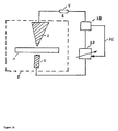
- FIG. 1 A shows a possible realisation, in which the voltage is controlled by a process controlled and optionally current limiting high voltage p ower supply. Depending on the p roperties/control characteristics of the voltage source, the current may also be limited by an optional resistor R, which is in series with the substrate.
- CDEB duration and consequently voltage application is e.g. set by a timer which is triggered at a p reset trans-substrate current level usually indicating the onset of the DEB process.
- the onset of the DEB process is indicated by a very steep and strong current increase. Because of the exponential nature of this current increase during DEB, CDEB requires a fast trigger.
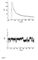
- Figure 3A shows a micro hole formed with CDEB in polypropylene (upper panel) as well as the current-voltage trace recorded when the trans-substrate voltage was raised to the critical DEB value (lower panel). Smaller holes (diameter ⁇ 1 um) were consistently produced by further limiting the current upon an increase in the series resistance R.
- the distance between the electrodes and carrier to be structured can be varied. If the electrodes touch the substrate ('contact mode'), the necessary DEB voltage is reduced to a minimum. However, contaminations and mechanical influences on the substrate deriving from the electrodes may occur. Using a gap between the substrate material and the electrodes may increase the necessary DEB voltage, reduces however the risk of electrode interferences with the substrate surface.
- a gap between substrate surface and electrode allows for the ionization of the gas molecules between them, providing the means for a modification of the substrate surface through activated gas molecules.
- the gas composition between the electrodes and substrate is controlled in such a way that during DEB the ionized gas molecules interact with the substrate surface in a manner beneficial for the intended application (e.g. cell adhesion).
- An example is the usage of pure oxygen which leads to the generation of activated oxygen molecules/ions/radicals during DEB which in turn can oxidize the substrate surface.
- Another way to concurrently modify the surface during DEB is the prior coverage of the surface with materials that, upon the ionization and heating process during DEB, undergo a chemical modification beneficial for the application of the substrate (e.g. for better membrane adhesion).
- the surface properties of the CDEB formed hole and its surroundings can also be controlled by selection of a substrate material that during DEB is fully or in part transformed into a material of choice.
- the electrodes can be surrounded by an insulating material such as PDMS (polydimethyl siloxane) that also tightly seals to the substrate surface.
- PDMS polydimethyl siloxane
- Another possibility of avoiding DEB processes bypassing the substrate is the usage of substrates surrounded by media that have a much higher breakdown voltage than the substrate material itself (e.g. silicon oil).
- the electrodes may also be surrounded by liquids of various dielectric properties (e.g. water, dichloromethane) to modify the DEB outcome as well as to modify the temperature distribution at the structuring site.
- the classical DEB method as well as the here described CDEB method still lack the ability to perforate most substrates of interest, e.g. substrates that do not easily melt/burn, have crystalline structures, are to brittle or require DEB voltages that are not useable for substrates in practice (glass, quartz).
- the necessary DEB voltage must be decreased or at least modulated and, in some cases, material properties must be changed or initialized before the actual DEB hole production process takes place so that the material is e.g. soft enough as not to b reak during hole production (e.g. g lass).
- CDEB structuring can be applied to essentially any insulating material, since all insulators show at some specific electric field strength a full or partial transition into a conducting state. Consequently, a wide selection of substrate materials ought to exist allowing for an optimal selection of substrate/carrier parameters such as membrane and cell adhesion and electric/dielectric properties for e.g. Patch Clamp on a Chip applications.
- the reduction of the insulator-to-conductor transition field strength by raising the substrate temperature is a central part of this invention.
- Heating the substrate either extrinsically with an additional external energy source or intrinsically by e.g. dielectric losses caused by AC voltage components before CDEB takes place, can both sufficiently reduce the required DEB voltage and alter the material properties so that materials, where the dielectric breakdown point is usually difficult to achieve or side effects come into play, can be microstructured.
- heating can be locally restricted.
- Heating the substrate or usually parts thereof in a defined manner makes materials accessible to CDEB that usually can not be modified at a useable thickness or that tend to break because of brittleness at normal (ambient) temperatures.
- making round holes in glass cover slides (e.g. Menzel S1) by 'normal' CDEB is virtually impossible due to the required high voltages and also the breakage of the glass slides once DEB takes place at these high voltages; injecting an appropriate amount of additional heat at the intended CDEB site reduces the electric resistance sufficiently to initiate DEB leading to round and largely smooth holes in the slide.
- An intended effect of this method is the production of high aspect ratio holes. Because the necessary DEB voltage is lowered by heat injection, relatively thick substrates (compared to e.g.
- the invention claims the particular use of this thermally supported DEB process.
- a heat source is added to the perforation device ( Figure 1B , 1C , 1D ).
- Heating the substrate can achieve the following: (I) softening (if necessary up to the point of melting) of the substrate material or parts thereof (II) reduction of the necessary DEB voltage caused by a lowered electrical resistance of the substrate.
- the heat and energy source can inject energy/heat in different ways. It is possible to apply energy/heat from one or both sides (referring to the position of the electrodes) of a substrate.
- Various heat sources are suitable, e.g. lasers ( Figure 1C , e.g. infrared laser for glass), heating filaments ( Figure 1B ) and flames. Due to the fact that flames consist of (partially) ionized gas molecules and consequently have a higher electrical conductivity than cold gas (e.g. surrounding air) they can be used as an electrode for the voltage application during CDEB ( Figure 1D ). For this reason a metal or other electrically conducting part which is in contact with the flame (e.g. the metal opening of the burner releasing the flame) is connected to the DEB voltage source.
- the invention claims the use of directed and locally restricted heating of the substrate with the goal to induce only locally the above described heating effects on the substrate material and consequently direct the location of the CDEB process on the substrate.
- the flame of a gas burner is focussed and positioned at the substrate surface where the hole is to be formed ( Figure 1D ).
- a laser spot can be positioned at the substrate surface ( Figure 1C ).
- the combination of high precision laser spot positioning and normal CDEB defines a device and method for high precision CDEB micro-perforation.
- the invention claims that (locally) adjusting the substrate temperature to specific levels or ranges is a way of controlling the hole/channel properties. This becomes immediately clear considering e.g. the differences in viscosity, surface tension and electrical resistance of the substrate material at different temperatures. Also the control of the heat distribution across the carrier is an additional method to modulate the CDEB outcome on the hole/channel properties. Appropriate ways of controlling the heat distribution involve the size and placement of the heat source (e.g. heating filament size and distance to the substrate surface), the amount heat coupling from the heat source into the substrate per time unit as well as the duration and possibly modulation of the heat application.
- the heat source e.g. heating filament size and distance to the substrate surface
- the deposition process can be combined with the CDEB process.
- the substrate may be 'clamped' at some locations to certain constant heat reservoirs to maintain the desired heat distribution.
- An additional function can be assigned to substrate heating and is part of this invention, which may occur either by an extrinsic heat source or an appropriate trans-substrate/trans-hole current generated after CDEB.
- the produced structures can be post-processed by melting/annealing/tempering. This is an appropriate way to e.g. change the diameter of CDEB produced holes, to smoothen the surface roughness inside and outside the hole mouth or to eliminate mechanic tensions of the material surrounding the hole. In tests, the hole diameter could be reduced up to a factor 1.6 (as determined by conductance measurements in saline solution) by such a prolonged heat application.
- Substrate heating and CDEB can be combined in various ways to achieve the desired holes/channels and surface properties.
- the invention uses most commonly: (I) heating of the substrate to a preset value and consequent application of the DEB voltage and (II) application of a specific DEB voltage and heating of the substrate until DEB occurs.
- heat and voltage may be reduced after DEB with or without a delay in a way suited for the CDEB process, e.g. abrupt reduction or 'fading' out.
- the formed structures may be post-processed. For instance, the heat produced by the electric arc passing the substrate at a hole site modifies the hole by melting surface material. That way, the structure itself as well as its surface properties can be modified.
- a very simple and elegant way of combining substrate heating source and DEB source is the u se of a s ingle modulated or alternating voltage source.
- This method consists of at least two components: (1) local heating of the substrate through (1A) dielectric losses of the substrate material induced by a changing voltage/electrical field across this substrate region and/or (1B) through electric arcs forming between the electrodes and substrate surface and (2) DC voltage induced normal CDEB.
- a suitable device employing this method can consist of only two electrodes, which are connected to a controlled voltage source providing the necessary AC-DC voltage superposition -as well as any kind of a sufficiently insulating mechanic support for the substrate ( Figure 1A and 2 ).
- the invention claims the use of electric arcs forming at sufficiently high AC voltage amplitudes and frequencies capable of heating localized substrate areas sufficient for DC voltage supported DEB hole formation.
- substrate material at the structuring site is sufficiently softened or even molten before the actual hole producing CDEB step takes place.
- heat initialization In particular for brittle or crystal materials this becomes important. If this is not taken into account, the substrate may break because of brittleness (usually at the structuring site) and become unusable.
- the voltages can sometimes still be raised until DEB occurs, usually causing material to break out of the substrate, forming a brittle structure not useable for most applications. For instance, this can be observed when placing a thin glass slide between closely spaced high voltage electrodes (e.g.
- a special and very useful realisation of this invention is the usage of alternating or modulated voltages with no or only small DC components for CDEB.
- an AC voltage is applied across the substrate region to perforate.
- the dielectric losses of the substrate upon this AC field/voltage application and/or the electric arc which may form lead to such a strong local substrate heating that a hole can form through the substrate (i.e. essentially pointing from one electrode to the other).
- the actual hole causing process usually occurs through thermally induced very sudden volume increase as well as evaporation of the substrate material, which in turn leads to an 'ejection' of liquid and gaseous substrate material out of the forming hole structure.
- the subsequent pulses of the train differ in AC power and frequency and trigger current
- reducing the AC frequency from 60 kHz to 20 kHz during the pulse train improved the hole quality.
- pulse trains were applied repeatedly, with each train termination triggered by DEB onset (i.e. t rigger current level reached), yielding very small (diameter ⁇ 2 um) and open holes in e.g. Menzel S1 glass slides. With the same cover slides it was observed that only at 'parameter islands' open holes were produced. In between, holes were probably closed by tiny a mounts of molten g lass moving into the center of the hole, probably by surface tension.
- CDEB parameters can be chosen such as to combine heat initialization and perforation step.
- CDEB methods can be combined with an additional tempering step.
- large mechanical tensions can form inside the substrate (e.g. with glass) at the hole location. Moving the substrate temperature up, e.g. in the range of the substrate softening temperature, usually reduces these tensions rendering the substrates long term stable and widely applicable.
- Increasing the frequency of the AC voltage component is a method to better define the location of the forming substrate hole. This becomes immediately apparent considering the fact that the capacitive current component of the current flowing between the perforation electrodes increases with increasing frequency while the ohmic current stays essentially unchanged so that the overall current, which is increasingly dominated by the capacitive component, follows the direct way between the electrodes, more and more unaltered by ohmic obstacles. Since the capacitive current does not necessarily follow the ohmic path (i.e. lowest ohmic resistance), already existing holes or cavities and other structural or material property inhomogeneities lead to lesser deviations of the current path and consequently to a more precise hole location with increasing frequency. This extends the method to multiple perforations of one substrates with holes closely spaced.
- the usage of higher AC frequencies leads to a method suited for the production of e.g. high density arrays of micro cavities and other structures (e.g. surface channels) suited for applications in these fields.
- the CDEB process is either terminated before full opening of the hole or prolonged so that the hole is closed again with molten substrate material. Moving the substrate during CDEB leads to the formation of channels. For these latter purposes the intrinsically heat supported CDEB method is clearly preferred.
- micro-structured carriers made by thermally supported CDEB with the means for electrophysiological measurements provides the basis for new and inexpensive devices monitoring electrical currents through biological membranes.
- the carrier separates two or more fluid compartments that are only connected through the CDEB produced hole.
- the biological membranes to be analysed are placed on one side of the carrier across the hole sealing it tightly.
- Figure 4 illustrates the usage of a CDEB micro structured carrier as support for an artificial lipid membrane in a BLM set-up; the lipid membrane is usually provided by a giant unilamellar vesicle positioned at the hole opening.
- Figure 5 illustrates the usage of a micro structured carrier, processed by thermally supported CDEB, as support for a patch clamp type set-up with biological cells.
- Figure 1A is a schematic diagram (side view) illustrating an embodiment of a device for CDEB based manufacturing of defined micro structures such as holes, consisting of the insulating substrate material to be structured (1) between electrodes (2); the electrodes can have various forms (2) and distances to the substrate material; the electrodes are connected to an adjustable and process controlled high voltage source (3); the latter consists of an adjustable voltage source (3A) receiving feedback (3C) from a current monitor (3B) that modifies, that is, usually disables, voltage source output after a preset d elay (delay usually zero or near zero) once a specified trans-substrate current (or current pattern) has been reached (DEB onset). Trigger level and voltage source properties are usually set or programmed by the operator.
- An optional series resistance R (4) may be connected in series with the electrodes to limit the current during CDEB.
- a series resistor is particularly useful when only very small currents are permissible for substrate perforation and stray capacitances and/or timing of the voltage source render the precise current control difficult and imprecise, respectively.
- the voltage source usually controls the CDEB process in such a way that the maximum current and the duration of current flow after DEB onset is adjusted.
- DEB onset can be detected in various ways; most suitably, DEB is usually detected by a trigger monitoring the trans-substrate current. In a preferred embodiment, a steep increase in this current by usually more than one order of magnitude indicates DEB onset.
- the substrate material and electrodes may be surrounded by a controlled gas composition and pressure (5).
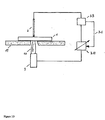
- FIG. 1B illustrates an embodiment of a device for extrinsically heat supported CDEB.
- Heat is supplied by a heating filament (6) controlling the substrate temperature.
- the heating filament also serves as counter electrode (6).
- the electrode (6) is directly heated by an electric current applied to terminals (7).
- the heated electrode was connected to ground while the opposite electrode supplied the voltage ("hot" end).
- the electrode (6) can also be indirectly heated by surrounding the electrode with a suitable heating element.
- One realisation used to produce holes of 1 - 10 um diameter in Menzel S1 cover slides consisted of a feedback controlled 0- 30 kV, 0 - 300 uA voltage source, connected to a 0.1 - 2 mm Pt-wire electrode on one side of the slide (distance ca.
- Figure 1C illustrates an embodiment of a device for extrinsically heat supported DEB.
- the substrate temperature is locally controlled by a laser (8, beam indicated as dashed line). Additionally, a pyrometer can be used to supply feedback to the laser for precise substrate temperature adjustment.
- D EB is initiated by a short laser pulse.
- the voltage source (3) is controlled according to the description of Figure 1A .
- Figure ID illustrates an embodiment of a device for extrinsically heat supported DEB based on a device as in Figure 1A (resistance omitted for simplicity) with a modified electrode (2).
- One electrode (2) is replaced by a burner (9) focussing a flame (10) onto the substrate surface.
- Undesired global heating and deformation of the substrate can b e avoided b y h eat shields (11), e.g. Schott CERANTM plates, providing only restricted access to the substrate surface (usually recommended is a second heat shield (11) on top of (1) avoiding heat caused deformations of (1)).
- the flame outlet of the burner is metallic it can be directly connected to the feedback controlled high voltage DEB source (3).
- FIG. 2A is a schematic diagram illustrating a possible embodiment of a current-voltage source for formation of CDEB structures, such as holes for carriers of biological membranes.
- the operator (1) sets via a computer (2) with attached digital-analog/analog-digital converter (3) the voltage (4) and maximum current (4) of the controllable high voltage source (6) (e.g. EuroTest CPP300304245, Germany). Voltage is applied to the carrier (9) via electrodes (8) and an optional current limiting resistor (7).
- the resistor may be necessary when the internal current limitation of the voltage source is not precise or does not respond quickly enough for some substrates or large capacitances in parallel to the electrodes render the current limitation circuits of the voltage source inefficient for quick response.
- the current through the substrate (9) is monitored by the computer via a current monitoring signal ( 5) coming from a current monitor, which may be part of the voltage source.
- a current monitoring signal coming from a current monitor, which may be part of the voltage source.
- a timer is triggered that sets the duration of the controlled current flow. This consequently sets the electric energy at a given voltage, which is partially transformed into heat energy, driving the actual hole forming process.
- the current flow interval after DEB detection can be set to zero.
- FIG. 2B is a schematic diagram illustrating a possible embodiment of a current-voltage source for intrinsically heat supported CDEB based on AC voltages only.
- the DEB voltage electrodes (2) are connected to ground and the output of a high voltage transformer (3, e.g. flyback transformer without rectifier from CRT type monitor), respectively.
- the transformer output is also grounded via a resistor (4), serving as trans-substrate current monitor.
- the transformer is driven via a transistor (5, e.g. IGBT or power npn).
- the transistor is driven by pulse trains usually received from a computer controlled AD/DA converter.
- the increased trans-substrate current leads to an increased voltage drop across (4) which is sensed by the trigger (8).
- the trigger signal (activ Low!) disables via an AND gate (7) the transistor (5) and consequently further high voltage generation, even if the computer did not yet process the trigger signal (10).
- the voltage drop across (4) and consequently trans-substrate current at which high voltage generation is stopped is set by the trigger level line (12).
- Figure 3A shows a microscopic image (upper picture) of a hole produced with CDEB in a 20 um thick polypropylene (PP) sheet.
- the hole diameter is ca. 5 um (aspect ratio ca. 4).
- the lower part shows the current-voltage curve (uA - kV) recorded while the trans-substrate voltage was increased until DEB occurred.
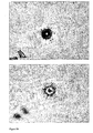
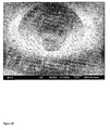
- Figure 3B shows microscopic images of holes produced with thermally supported CDEB (according to Figure 1D ) in a ca. 170 um thick glass cover slide.
- the hole diameter is ca. 3 um.
- Upper picture torch side of the substrate/hole; lower picture: opposite side of the substrate/hole.
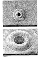
- Figure 3C s hows electron microscopic images of the heating filaments ide of holes produced with thermally supported C DEB (according t o Figure 1B ) in a ca. 170 um thick glass cover slide (Menzel S1) at different magnifications (upper panel 1500x/lower panel 5000x, scale bar see figure). At 1500x, glass filaments ejected during CDEB and now covering the substrate surface are visible.
- Figure 3D shows an electron microscopic image of the voltage electrode side of holes produced with thermally supported DEB (according to Figure 1B ) in a ca. 170 um thick glass cover slide (Menzel S1, scale bar see figure).
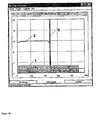
- Figure 3E shows the time course of the current (3) - voltage (2) relationship during the thermally supported perforation of a standard microscopic cover slide (Menzel S1 20x20) with a pure DC voltage (vertical axis indicating kV and 30*uA, i.e. maximum substrate current shown is 600 uA, horizontal axis in milliseconds).
- the DEB process is initiated by a short heating pulse using a Pt filament (ca. 1x1 mm2 active area parallel to the slide surface) mounted c lose (ca. 0.3 m m) to the slide surface.
- the heating filament serves also as ground electrode.
- the voltage electrode was mounted ca 0.5 mm from the cover slide opposite the ground electrode.
- the current heating the filament is indicated (1).
- the filament heating current interval was preset; the DC voltage of ca. 12 kV was shut-down immediately after dielectric breakdown detection.
- the trigger signal used for this shut-down was a sudden raise of several orders of magnitude of the substrate current (3) accompanying the hole formation (see figure at ca. 530 ms).
- the hole was ca. 3 um in diameter (aspect ratio ca. 50).
- This cover slide was used in a patch clamp setup and produced a giga seal with Jurkat-cells in Ringer solution within less than 5 sec after moving of a cell over the hole by suction.
- the optimal heating current was determined experimentally and is shown in arbitrary units; heat produced by the Pt-filament was controlled by the duty cycle of the 5V/10 kHz heating power supply.
- Figure 3F depicts the conditions during a combined AC - DC voltage produced CDEB.
- the AC voltage was supplied intermittently (two series of 10 pulses of 60 and 40 ms (2 nd series shown), respectively, with 5 ms between AC pulses; pulse 10 not applied because of trigger signal induced AC and DC shut down) to better control the substrate heating process, thus avoiding micro cracks in the substrate caused by mechanical tensions.
- the AC current induced heating of the substrate leads to a dielectric breakdown during which substrate material is ejected leading to a ca. 3 um hole (aspect ratio ca. 50) and usually the deposition of thin filaments ejected from the hole on the substrate surface.
- a strong increase in AC current during DEB was used as trigger signal for immediate AC and DC voltage shut down to avoid closing the hole by excess molten glass.
- DEB also leads to a typical increase in DC current (3).
- Substrate Cover slide (Menzel S1 18x18). The horizontal axis is in milliseconds, the vertical axis shows V in kV units and current in uA*30, the maximum substrate current (DC component) shown is 600 uA.
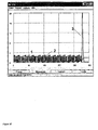
- Figure 3G depicts the time course of a hole formation by intrinsically heat supported CDEB (AC only) in a standard microscopic cover slide (Menzel S1).
- the AC current flowing through the primary coil of a high voltage transformer during substrate structuring is shown (1).
- the current flow as well as electric arcs between the electrodes and the substrate as well as dielectric losses inside the substrate lead to a fast (nearly approaching exponential growth) temperature increase causing melting, evaporation and ejection of substrate material out of the forming hole. This material can be found as thin filaments at the substrate surface.
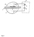
- Figure 4 shows a possible realisation of a device using CDEB micro structured carriers for electrical membrane measurements.
- the carrier (1) separates two fluid compartments having any shape and boundaries (8, 9) which are only connected through the carrier channel (2) formed by CDEB.
- One side of the channel is covered by a biological membrane (3).
- voltages applied through the fluid immersed (redox) electrodes (4) lead to a current that is only dependent on the properties of the biological membrane it self.
- Current voltage measurements may be performed with a suitable device (5) allowing to set the voltage (6) and measure the current (7).
- the device (5) may be substituted with a voltage measuring device.
- Figure 5 shows a possible realisation of a device using CDEB micro structured carriers for electrical membrane measurements on biological cells such as patch clamp measurements.
- the carrier (1) separates two fluid compartments (6, 7) which are only connected through the CDEB produced channel (2).
- One side of the channel is covered by a biological cell (3).
- voltages applied through the fluid immersed (redox) electrodes (4) lead to a current that is only dependent on the properties of the cell membrane.
- redox fluid immersed
- Current voltage measurements may be performed with a suitable device (5), such as a patch clamp amplifier (e.g. Axon Instruments).
- Figure 6 illustrates the sealing process of a K562 cell to a CDEB produced carrier used in a patch clamp configuration (upper panel) and subsequent single channel recordings in cell attached mode (lower panel).
- Menzel S1 cover slides were perforated using an intrinsically heat supported CDEB process (AC only, train of 4 pulses with 200 ms duration separated by 100 ms off-time, V c a. 20 000 V at 40 kHz, t rigger current (here, the current through the primary coil of the high voltage transformer was monitored) was linearly raised form 2000 mA (first pulse) to 2400 mA (last pulse), pointed palladium electrodes with 2.5 mm electrode distance; the slide was tempered after hole formation by short (ca.
- AC intrinsically heat supported CDEB process
Landscapes
- Life Sciences & Earth Sciences (AREA)
- Forests & Forestry (AREA)
- Engineering & Computer Science (AREA)
- Mechanical Engineering (AREA)
- Physics & Mathematics (AREA)
- Optics & Photonics (AREA)
- Physical Or Chemical Processes And Apparatus (AREA)
- Immobilizing And Processing Of Enzymes And Microorganisms (AREA)
Claims (65)
- Verfahren zum Bilden eines Lochs oder Höhlung oder Kanals in einer Region eines elektrisch isolierenden Substrats (1), umfassend die Schritte:a) Bereitstellen eines elektrisch isolierenden Substrats (1),b) Anlegen einer Spannung mittels einer Spannungsquelle (3) an eine Region des elektrisch isolierenden Substrats, wobei die Spannung ausreicht, um einen signifikanten Anstieg an elektrischem Strom durch die Region und einen dielektrischen Durchschlag (DEB) durch die Region zu verursachen,c) Aufbringen von Wärme auf die Region, um die Temperatur der Region zu erhöhen, um die Stelle zu definieren, an der ein dielektrischer Durchschlag stattfinden soll, wobei die Wärme entweder aus einer Energie- oder Wärmequelle oder aus Bestandteilen der Spannung stammt, die in Schritt b) angelegt wird, wobei die Wärme so aufgebracht wird, dass die Amplitude der Spannung verringert wird, die in Schritt b) erforderlich ist, um den Anstieg des Stroms durch die Region zu verursachen,wobei das Verfahren auf eine solche Weise durchgeführt wird, dass Substratmaterial in der Region hinreichend aufgeweicht oder geschmolzen wird, bevor ein Loch-produzierender Schritt eines kontrollierten dielektrischen Durchschlags (CDEB) stattfindet, und wobei
Schritt b) unter Verwendung eines elektronischen Feedback-Mechanismus durchgeführt und beendet wird, der gemäß Benutzer-vordefinierten Parametern betrieben wird, wobei der elektronische Feedback-Mechanismus die Eigenschaften der angelegten Spannung und/oder des elektrischen Stroms kontrolliert,
dadurch gekennzeichnet, dass der elektronische Feedback-Mechanismus einen Analyseschaltkreis umfasst, der ein Strom-Analyseschaltkreis oder ein Spannungs- und Strom-Analyseschaltkreis ist, allein oder als Teil einer Benutzer-programmierten Vorrichtung, wobei der Analyse-Schaltkreis in der Lage ist, die Ausgangsparameter der Spannungsquelle in Bezug auf eine Spannung durch das Substrat und einen Stromfluss gemäß Benutzer-vordefinierten Prozeduren zu kontrollieren, und weiterhin dadurch gekennzeichnet, dass in Schritt c) Wärme in einer gerichteten und lokal beschränkten Weise nur auf die Region aufgebracht wird. - Verfahren nach Anspruch 1, wobei der elektronische Feedback-Mechanismus ein Ende des Schrittes b) innerhalb einer Benutzer-vordefinierten Periode nach Beginn des dielektrischen Durchschlags bewirkt, wobei der Beginn bevorzugt ein Anstieg der Anzahl an Ladungsträgern pro Zeiteinheit um einen Faktor von 2, bevorzugt um wenigstens eine Größenordnung ist.
- Verfahren nach einem der vorangehenden Ansprüche, wobei der signifikante Anstieg an elektrischem Strom ein Anstieg in der Anzahl der Ladungsträger pro Zeiteinheit um einen Faktor von 2, bevorzugt um wenigstens eine Größenordnung ist.
- Verfahren nach einem der Ansprüche 2-3, wobei der elektronische Feedback-Mechanismus bewirkt, dass das Ende des Schrittes b), mit oder ohne eine voreingestellte Verzögerung, zu dem Zeitpunkt stattfindet, wenn der elektrische Strom einen Schwellenwert erreicht hat, bevorzugt im Bereich von 0,01 bis 10 mA, oder zu dem Zeitpunkt, wenn ein Anstieg des elektrischen Stroms, (dI/dt), einen Schwellenwert erreicht hat, bevorzugt gleich oder größer als 0,01 A/s.
- Verfahren nach einem der vorangehenden Ansprüche, wobei der elektronische Feedback-Mechanismus schnell genug ist, um ein Ende des Schrittes b) innerhalb einer Periode im Bereich von 1 ns bis 100 ms, bevorzugt von 1 ns bis 100 us, bevorzugter von 100 ns bis 10 us, nach dem Beginn des dielektrischen Durchschlags verursachen zu können, oder innerhalb der zuvor erwähnten Periode, nachdem der Anstieg des elektrischen Stroms den Schwellenwert erreicht hat.
- Verfahren nach Anspruch 5, wobei der elektronische Feedback-Mechanismus ein Ende des Schrittes b) innerhalb einer Periode im Bereich von 100 ns bis 10 s, bevorzugt von 100 ns bis 1 s, nach dem Beginn des dielektrischen Durchbruchs oder nachdem der Anstieg des elektrischen Stroms den Schwellenwert erreicht hat, bewirkt.
- Verfahren nach einem der Ansprüche 2-6, wobei das Ende des Schrittes b) ohne einen Eingriff durch einen Benutzer stattfindet, sobald Schritt b) initiiert worden ist.
- Verfahren nach einem der vorangehenden Ansprüche, wobei der Analyse-Schaltkreis in der Lage ist, die Energie- oder Wärmequelle, sofern vorhanden, zu kontrollieren.
- Verfahren nach einem der vorangehenden Ansprüche, wobei die Schritte b) und c) zusammen stattfinden.
- Verfahren nach einem der vorangehenden Ansprüche, wobei Schritt c) unter Kontrolle eines Benutzers stattfindet, bevorzugt unter Verwendung des elektronischen Feedback-Mechanismus.
- Verfahren nach Anspruch 10, wobei die Kontrolle eines Benutzers das Definieren oder die Regulierung der Menge und/oder der Dauer der Wärme beinhaltet, die auf die Region in Schritt c) aufgebracht wird.
- Verfahren nach einem der vorangehenden Ansprüche, wobei der elektronische Feedback-Mechanismus eine Regulierung der Amplitude und/oder der Dauer der Spannung und/oder des Stroms ermöglicht.
- Verfahren nach einem der vorangehenden Ansprüche, wobei die Spannung im Bereich von 102 V bis 106 V liegt, bevorzugt im Bereich von 103 V - 105 V.
- Verfahren nach einem der vorangehenden Ansprüche, wobei Schritt c) vor Schritt b) begonnen wird.
- Verfahren nach einem der vorangehenden Ansprüche, wobei Schritt c) fortgesetzt wird, nachdem Schritt b) beendet worden ist.
- Verfahren nach einem der vorangehenden Ansprüche, wobei Schritt b) stattfindet, indem Elektroden an die Region oder in deren Nähe gebracht werden, bevorzugt indem eine Elektrode auf eine Seite des Substrats gebracht wird und indem eine andere Elektrode auf eine andere Seite des Substrats gebracht wird, und indem die Spannung über die Elektroden angelegt wird.
- Verfahren nach einem der vorangehenden Ansprüche, wobei am Beginn des Schrittes b) die Spannung in der Amplitude bis auf einen Wert gesteigert wird, bei dem ein Anstieg an elektronischem Strom durch die Region stattfindet und/oder bei dem ein dielektrischer Durchbruch (DEB) durch das Substrat stattfindet und/oder bei dem ein elektrischer Bogen auftritt.
- Verfahren nach einem der vorangehenden Ansprüche, wobei der Strom entlang eines Stromwegs durch die Substratregion fließt und die Viskosität und/oder Steifheit und/oder Sprödigkeit des Substrats entlang und nahe dem Stromweg verändert.
- Verfahren nach Anspruch 18, wobei der Strom das Substrat entlang und nahe dem Stromweg aufweicht und/oder schmilzt und/oder verdampft, und/oder wobei der Strom und/oder die angelegte Spannung das Entfernen von Substratmaterial entlang und nahe dem Stromweg bewirkt, bevorzugt mittels Verdampfung, Auswurf, elektrostatischer Anziehung oder einer Kombination davon.
- Verfahren nach einem der Ansprüche 18-19, wobei Schritt b) nicht zu einem Brechen des Substrats führt, und wobei bevorzugt der Strom, der Stromanstieg und die Spannungsparameter durch einen Benutzer auf Werte begrenzt werden, wobei die Werte bevorzugter experimentell für jedes Substratmaterial und/oder Substratmaterialklasse bestimmt werden, wobei bei diesen Werten kein Brechen des Substrats verursacht wird.
- Verfahren nach einem der vorangehenden Ansprüche, wobei die angelegte Spannung eine reine Gleichspannung (DC) ist.
- Verfahren nach einem der Ansprüche 1-20, wobei die angelegte Spannung eine reine Wechselspannung (AC) ist.
- Verfahren nach einem der Ansprüche 1-20, wobei die angelegte Spannung eine Überlagerung von Wechsel- und Gleichspannungen ist.
- Verfahren nach einem der Ansprüche 22-23, wobei die Frequenz der angelegten Wechselspannung im Bereich von 102 bis 1012 Hz, bevorzugt im Bereich von 5 x 10² bis 108 Hz, bevorzugter 1 x 10³ bis 1 x 10⁷ Hz ist.
- Verfahren nach einem der Ansprüche 22-24, wobei die Wechselspannung in intermittierender Weise angelegt wird, bevorzugt in Puls-Stößen mit einer Dauer im Bereich von 1 ms bis 1000 ms, bevorzugt 10 ms bis 500 ms, mit einer Pause dazwischen mit einer Dauer von wenigstens 1 ms, bevorzugt wenigstens 10 ms.
- Verfahren nach einem der Ansprüche 22-25, wobei die angelegte Wechselspannung verwendet wird, um Schritt c) durchzuführen.
- Verfahren nach einem der Ansprüche 22-26, wobei die angelegte Wechselspannung Parameter hat (z. B. Amplitude, Frequenz, Tastgrad), die ausreichen, um einen elektrischen Bogen zwischen einer Oberfläche des Substrats und den Elektroden herzustellen.
- Verfahren nach Anspruch 27, wobei der elektrische Bogen dazu verwendet wird, um Schritt c) durchzuführen.
- Verfahren nach einem der Ansprüche 26-28, wobei die angelegte Wechselspannung zu dielektrischen Verlusten in der Region des Substrats fühlt, wobei die dielektrischen Verluste ausreichen, um die Temperatur der Region zu erhöhen.
- Verfahren nach einem der Ansprüche 22-29, wobei die Frequenz der angelegten Wechselspannung erhöht wird, um Abweichungen des Stromwegs von einer geraden Linie zwischen den Elektroden zu verringern.
- Verfahren nach einem der Ansprüche 22-30, wobei die Frequenz der angelegten Wechselspannung erhöht wird, um die mögliche Distanz zwischen benachbarten Strukturen, bevorzugt benachbarten Löchern zu minimieren.
- Verfahren nach einem der vorangehenden Ansprüche, wobei in Schritt c) Wärme an die Region des Substrats unter Verwendung einer beheizten Elektrode oder eines Heizelements angebracht wird, welches in der Nähe der Elektrode platziert ist.
- Verfahren nach Anspruch 32, wobei die beheizte Elektrode ein elektrisches Heizfilament ist und auch dazu verwendet wird, um die Spannung an der Region in Schritt b) anzulegen.
- Verfahren nach einem der vorangehenden Ansprüche, wobei in Schritt c) Wärme auf die Region des Substrats angebracht wird zusätzlich oder nur unter Verwendung einer externen Wärmequelle, wie etwa eines Lasers oder einer anderen fokussierten Lichtquelle, oder unter Verwendung einer Gasflamme.
- Verfahren nach einem der vorangehenden Ansprüche, wobei in Schritt c) Wärme auf die Region des Substrats durch Anlegen einer Wechselspannung an die Region angebracht wird.
- Verfahren nach Anspruch 35, wobei die Wechselspannung an die Region mittels Elektroden angelegt wird, die auf gegenüberliegenden Seiten des Substrates platziert sind, wobei bevorzugt wenigstens eine Elektrode auf einer Seite des Substrats platziert ist und wenigstens eine Elektrode auf einer anderen Seite des Substrats platziert ist.
- Verfahren nach Anspruch 36, wobei die Elektroden, die auf einander gegenüberliegenden Seiten des Substrates platziert sind, auch zum Durchführen von Schritt b) verwendet werden.
- Verfahren nach einem der Ansprüche 35-37, wobei die Wechselspannung ausreicht, um dielektrische Verluste in der Region des Substrats zu bewirken, was zu einem Steigen der Temperatur in der Region führt.
- Verfahren nach Anspruch 38, wobei die Wechselspannung im Bereich von 103 V - 106 V, bevorzugt 2 x 10³ V - 105 V liegt, und eine Frequenz im Bereich von 102 Hz bis 1012 Hz, bevorzugt im Bereich von 5 x 10² bis 108 Hz, bevorzugter 1 x 10³ bis 1 x 10⁷ Hz hat.
- Verfahren nach einem der vorangehenden Ansprüche, wobei die Struktur, die gebildet wird, ein Loch mit einem Durchmesser im Bereich von 0,01 µm bis 50 µm, bevorzugt 0,1 µm bis 10 µm und bevorzugter 0,3 µm bis 5 µm ist.
- Verfahren nach einem der Ansprüche 1-39, wobei die Struktur, die gebildet wird, eine Höhlung mit einem Durchmesser im Bereich von 0,1 µm bis 100 µm ist.
- Verfahren nach einem der Ansprüche 1-39, wobei die Spannung mittels Elektroden angelegt wird, die auf einander gegenüberliegenden Seiten des Substrates platziert sind, und wobei die Struktur, die gebildet wird, eine kanalartige Struktur ist, die durch eine relative Bewegung der Elektroden im Verhältnis zu dem Substrat erhalten wird.
- Verfahren nach einem der vorangehenden Ansprüche, wobei die Struktur, bevorzugt das Loch, ein Seitenverhältnis größer 1, bevorzugt größer als 5 hat.
- Verfahren nach einem der vorangehenden Ansprüche, wobei das elektrisch isolierende Substrat ausgewählt ist aus einer Gruppe, umfassend Kohlenstoff-basierende Polymere, wie etwa Polypropylen, Fluorpolymere, wie etwa Teflon, Silizium-basierte Substrate, wie etwa Glas, Quarz, Siliziumnitrid, Siliziumoxid, Silizium-basierende Polymere, wie etwa Sylgard, halbleitende Materialien, wie etwa elementares Silizium.
- Verfahren nach einem der vorangehenden Ansprüche, wobei die Region, in der eine Struktur gebildet werden soll, eine Dicke im Bereich von 10-9 m bis 10-2 m, bevorzugt 10-7 m bis 10-3 m, bevorzugter 10-5 m bis 5 x 10⁻⁴ m, am bevorzugtesten > 10-6 m hat.
- Verfahren nach einem der vorangehenden Ansprüche, wobei das Substrat in Schritt a) innerhalb eines Materials (Feststoff, Flüssigkeit oder Gas) bereitgestellt wird, das mit einer Oberfläche des Substrats während der Schritte b) und/oder c) reagiert.
- Verfahren nach einem der vorangehenden Ansprüche, wobei nach Bildung der Struktur, eine Oberfläche der Struktur durch weiteres Aufbringen von Wärme, bevorzugt durch Aufbringen von Wärme während des Schrittes c) geglättet wird.
- Verfahren nach einem der vorangehenden Ansprüche, wobei nach Bildung der Struktur ihre Form darauffolgend durch weiteres Aufbringen von Wärme, bevorzugt durch Aufbringen von Wärme während Schritt c) geändert wird.
- Verfahren nach einem der Ansprüche 47-48, wobei das weitere Aufbringen von Wärme mittels eines elektrischen Bogens stattfindet, der zwischen zwei Elektroden gebildet wird, bevorzugt zwei Elektroden, die dazu verwendet werden, um Schritt b) durchzuführen.
- Vorrichtung zum Durchführen des Verfahrens nach einem der vorangehenden Ansprüche, umfassend wenigstens zwei Elektroden (2), die mit einer Spannungsquelle (3) verbunden sind, welche durch einen Strom durch das Substrat kontrolliert wird, und wobei die Vorrichtung weiterhin eine Analyse- und Kontrolleinheit umfasst, die Teil der Spannungsquelle sein kann,
dadurch gekennzeichnet dass sie weiterhin Mittel zum Aufbringen von Wärme auf das Substrat in einer gerichteten und lokal beschränkten Weise umfasst, wobei die Mittel eine Elektrode (2) oder besagte wenigstens zwei Elektroden (2,2), oder eine weitere Wärmequelle (6, 7, 8, 9, 10) sind, und
dadurch gekennzeichnet, dass die Analyse- und Kontrolleinheit einen Analyse-Schaltkreis umfasst, der ein Strom-Analyse-Schaltkreis oder ein Spannungs- und Strom-Analyse-Schaltkreis ist, alleine oder als ein Teil einer Benutzer-programmierten Vorrichtung, wobei der Analyse-Schaltkreis in der Lage ist, die Ausgangsparameter der Spannungsquelle in Bezug auf eine Spannung über das Substrat und Stromfluss gemäß Benutzer-vordefinierten Prozeduren zu kontrollieren, so dass das Verfahren auf eine solche Weise durchgeführt wird, dass Substratmaterial an der Region hinreichend aufgeweicht oder geschmolzen wird, bevor ein Loch-produzierender Schritt eines kontrollierten dielektrischen Durchbruchs stattfindet. - Vorrichtung nach Anspruch 50, wobei der Analyse-Schaltkreis in der Lage ist, das Mittel zum Aufbringen von Wärme zu kontrollieren.
- Vorrichtung nach einem der Ansprüche 50-51, wobei es keine zusätzliche Wärmequelle gibt.
- Vorrichtung nach einem der Ansprüche 50-52, weiterhin umfassend Mittel zum Aufnehmen und Halten des elektrisch isolierenden Substrats, während die Struktur in der Region des Substrats gebildet wird.
- Vorrichtung nach einem der Ansprüche 50-53, wobei die Spannungsquelle eine regulierte Spannungsquelle ist, die Feedback-Signale aus dem Prozess der Bildung einer Struktur erhält, wie etwa beispielsweise Stromfluss und Wärme, und anschließend die Spannungsparameter, wie etwa Amplitude, Frequenz und Tastgrad in einer vordefinierten, bevorzugt Benutzer-definierten, Weise einstellt, um die erwünschte Struktur zu erzeugen.
- Vorrichtung nach einem der Ansprüche 50-54, wobei das Mittel zum Aufbringen von Wärme ein elektrisches Heizfilament ist, bevorzugt kontrolliert durch die Kontrolleinheit von Anspruch 51.
- Vorrichtung nach einem der Ansprüche 50-54, wobei das Mittel zum Aufbringen von Wärme ein Laser oder eine andere fokussierte Lichtquelle oder eine hochenergetische Strahlungsquelle oder eine Flamme ist, zum Beispiel von einer Mikroflamme ("micro torch").
- Vorrichtung nach einem der Ansprüche 50-54, wobei das Mittel zum Aufbringen von Wärme eine Wechselspannungsquelle ist, die mit den wenigstens zwei Elektroden verbunden ist, oder, sofern vorhanden, mit weiteren Sätzen Elektroden.
- Vorrichtung nach Anspruch 57, wobei die Wechselspannungsquelle mit der Spannungsquelle von Anspruch 50 zu einer einzigen Spannungsquelle kombiniert ist, die in der Lage ist, eine Wechselspannungskomponente zu erzeugen, die einen Wechselstrom erzeugen kann, der ausreicht, um das Substrat zu erwärmen und bevorzugt einen dielektrischen Durchbruch durch das Substrat zu bewirken.
- Vorrichtung nach einem der Ansprüche 50-58, wobei eine Distanz zwischen den wenigstens zwei Elektroden im Bereich von 0,01 bis 60 mm, bevorzugt 0,1 bis 15 mm und bevorzugter zwischen 0,5 bis 8 mm liegt.
- Vorrichtung nach einem der Ansprüche 50-59, weiterhin umfassend das elektrisch isolierende Substrat in einer Position, die im wesentlichen zwischen den wenigstens zwei Elektroden ist und die dem Mittel zum Aufbringen von Wärme zugänglich ist.
- Vorrichtung nach einem der Ansprüche 50-60, weiterhin umfassend Mittel zum Vermeiden von elektrischen Bögen zwischen den Elektroden, die das Substrat umgehen, indem sie das umgebende Medium, z. B. Luft, ionisieren, wie etwa Gummisiegel oder Glasplatten, die eng an das Substrat anliegen und im Ergebnis die Distanz erhöhen, die ein elektrischer Bogen zwischen den Elektroden nehmen müsste, wenn er das Substrat umgeht.
- Vorrichtung nach einem der Ansprüche 50-61, weiterhin umfassend Mittel zum weiteren Modifizieren einer Oberfläche des Substrats mittels einer physikalischen Reaktion, die durch die Spannung und den Strom, der zum Bilden der Struktur verwendet wird, initiiert und/oder aufrechterhalten wird, oder mittels einer chemischen Reaktion mit einem zusätzlichen Material, das mit der Oberfläche des Substrats während des Prozesses der Strukturbildung reagiert.
- Vorrichtung nach Anspruch 62, wobei das Mittel zum weiteren Modifizieren der Oberfläche des Substrats ein Behälter zum Aufnehmen des Substrats und zusätzlich eines Mediums ist, wie etwa eines Gases oder einer Flüssigkeit, die das Substrat umgibt.
- Vorrichtung nach einem der Ansprüche 50-63, weiterhin umfassend Mittel zum Modifizieren der gebildeten Struktur in einem Nachverarbeitungsschritt durch Wärmeaufbringen auf das Substrat, um eine Substratoberfläche zu glätten und/oder die Größe der Struktur zu verändern.
- Vorrichtung nach einem der Ansprüche 50-64, weiterhin umfassend ein elektrisch isolierendes Substrat, in dem eine Struktur gebildet werden soll.
Priority Applications (1)
| Application Number | Priority Date | Filing Date | Title |
|---|---|---|---|
| EP10012452.8A EP2324975B1 (de) | 2004-04-01 | 2005-03-30 | Herstellung und Verwendung von mikroperforierten Substraten |
Applications Claiming Priority (3)
| Application Number | Priority Date | Filing Date | Title |
|---|---|---|---|
| CH2004000206 | 2004-04-01 | ||
| CH2004000279 | 2004-05-07 | ||
| PCT/EP2005/003319 WO2005097439A2 (en) | 2004-04-01 | 2005-03-30 | Manufacturing and use of microperforated substrates |
Related Child Applications (2)
| Application Number | Title | Priority Date | Filing Date |
|---|---|---|---|
| EP10012452.8A Division EP2324975B1 (de) | 2004-04-01 | 2005-03-30 | Herstellung und Verwendung von mikroperforierten Substraten |
| EP10012452.8 Division-Into | 2010-09-30 |
Publications (2)
| Publication Number | Publication Date |
|---|---|
| EP1744860A2 EP1744860A2 (de) | 2007-01-24 |
| EP1744860B1 true EP1744860B1 (de) | 2012-02-01 |
Family
ID=37684770
Family Applications (2)
| Application Number | Title | Priority Date | Filing Date |
|---|---|---|---|
| EP05716445A Expired - Lifetime EP1744860B1 (de) | 2004-04-01 | 2005-03-30 | Herstellung und verwendung von mikroperforierten substraten |
| EP10012452.8A Expired - Lifetime EP2324975B1 (de) | 2004-04-01 | 2005-03-30 | Herstellung und Verwendung von mikroperforierten Substraten |
Family Applications After (1)
| Application Number | Title | Priority Date | Filing Date |
|---|---|---|---|
| EP10012452.8A Expired - Lifetime EP2324975B1 (de) | 2004-04-01 | 2005-03-30 | Herstellung und Verwendung von mikroperforierten Substraten |
Country Status (4)
| Country | Link |
|---|---|
| US (1) | US8759707B2 (de) |
| EP (2) | EP1744860B1 (de) |
| AT (1) | ATE543617T1 (de) |
| WO (1) | WO2005097439A2 (de) |
Families Citing this family (31)
| Publication number | Priority date | Publication date | Assignee | Title |
|---|---|---|---|---|
| WO2007054220A1 (en) * | 2005-11-09 | 2007-05-18 | Christian Schmidt | Methods and devices for surface modification of micro-structured substrates |
| US7840537B2 (en) | 2006-12-22 | 2010-11-23 | Commvault Systems, Inc. | System and method for storing redundant information |
| US20100314723A1 (en) | 2007-07-20 | 2010-12-16 | Christian Schmidt | Manufacturing of optical structures by electrothermal focussing |
| WO2009059786A1 (en) * | 2007-11-09 | 2009-05-14 | Picodrill Sa | Electrothermal focussing for the production of micro-structured substrates |
| KR20110096060A (ko) | 2008-12-02 | 2011-08-26 | 피코드릴 에스 아 | 기판 내에 구조물을 도입하는 방법 |
| US8736026B2 (en) * | 2009-02-27 | 2014-05-27 | Picodrill Sa | Method of generating a hole or recess or well in a substrate |
| US8401996B2 (en) | 2009-03-30 | 2013-03-19 | Commvault Systems, Inc. | Storing a variable number of instances of data objects |
| US8578120B2 (en) | 2009-05-22 | 2013-11-05 | Commvault Systems, Inc. | Block-level single instancing |
| JP2013502704A (ja) * | 2009-08-19 | 2013-01-24 | ピコドリル エスアー | 基板に導電性ビアを製造する方法 |
| DE102010025967B4 (de) | 2010-07-02 | 2015-12-10 | Schott Ag | Verfahren zur Erzeugung einer Vielzahl von Löchern, Vorrichtung hierzu und Glas-Interposer |
| DE102010025968B4 (de) | 2010-07-02 | 2016-06-02 | Schott Ag | Erzeugung von Mikrolöchern |
| DE102010025965A1 (de) * | 2010-07-02 | 2012-01-05 | Schott Ag | Verfahren zur spannungsarmen Herstellung von gelochten Werkstücken |
| DE102010025969A1 (de) | 2010-07-02 | 2012-01-05 | Schott Ag | Locherzeugung mit Mehrfach-Elektroden |
| DE102010025966B4 (de) | 2010-07-02 | 2012-03-08 | Schott Ag | Interposer und Verfahren zum Herstellen von Löchern in einem Interposer |
| US8393175B2 (en) | 2010-08-26 | 2013-03-12 | Corning Incorporated | Methods for extracting strengthened glass substrates from glass sheets |
| US8935492B2 (en) | 2010-09-30 | 2015-01-13 | Commvault Systems, Inc. | Archiving data objects using secondary copies |
| WO2012133004A1 (ja) * | 2011-03-28 | 2012-10-04 | ピコドリル エスアー | 基板切断方法及び切断装置 |
| EP2564999A1 (de) | 2011-08-31 | 2013-03-06 | Asahi Glass Company, Limited | Verfahren zur Erzeugung eines Lochs oder einer Aussparung hoher Qualität in einem Substrat |
| EP2564996A1 (de) | 2011-08-31 | 2013-03-06 | Asahi Glass Company, Limited | Verfahren zur Erzeugung eines Lochs oder einer Aussparung oder eines Wells in einem elektrisch isolierenden oder halbleitenden Substrat |
| EP2812149A1 (de) * | 2012-02-10 | 2014-12-17 | Asahi Glass Company, Limited | Vorrichtung zum bohren eines substrats mit mehreren gleichspannungsausgängen sowie verfahren zum bohren eines substrats mit einer solchen vorrichtung |
| US9020890B2 (en) | 2012-03-30 | 2015-04-28 | Commvault Systems, Inc. | Smart archiving and data previewing for mobile devices |
| WO2014022681A1 (en) | 2012-08-01 | 2014-02-06 | Gentex Corporation | Assembly with laser induced channel edge and method thereof |
| US9633022B2 (en) | 2012-12-28 | 2017-04-25 | Commvault Systems, Inc. | Backup and restoration for a deduplicated file system |
| CO7010169A1 (es) * | 2013-01-29 | 2014-07-31 | Univ Nac De Colombia | Método y aparato para la perforación eléctrica de laminas |
| US10324897B2 (en) | 2014-01-27 | 2019-06-18 | Commvault Systems, Inc. | Techniques for serving archived electronic mail |
| JP6295897B2 (ja) * | 2014-09-05 | 2018-03-20 | 旭硝子株式会社 | ガラス基板に貫通孔を形成する装置および方法 |
| US10324914B2 (en) | 2015-05-20 | 2019-06-18 | Commvalut Systems, Inc. | Handling user queries against production and archive storage systems, such as for enterprise customers having large and/or numerous files |
| JP2017088467A (ja) * | 2015-11-16 | 2017-05-25 | 旭硝子株式会社 | ガラス基板に孔を形成する装置および方法 |
| CN106178138A (zh) * | 2016-09-07 | 2016-12-07 | 上海申淇医疗科技有限公司 | 一种药物球囊 |
| WO2018085249A1 (en) * | 2016-11-04 | 2018-05-11 | Corning Incorporated | Micro-perforated panel systems, applications, and methods of making micro-perforated panel systems |
| RU2702798C1 (ru) * | 2018-08-20 | 2019-10-11 | Федеральное государственное бюджетное учреждение науки, Институт Ядерной Физики им. Г.И. Будкера Сибирского отделения (ИЯФ СО РАН) | Способ изготовления высокоаспектных микроструктур |
Family Cites Families (11)
| Publication number | Priority date | Publication date | Assignee | Title |
|---|---|---|---|---|
| FR1418083A (fr) | 1964-08-07 | 1965-11-19 | Siderurgie Fse Inst Rech | Procédé et dispositif de marquage de matériaux |
| GB1089369A (en) | 1965-10-06 | 1967-11-01 | Meyer Lab Inc | Improvements in methods and apparatus for electrically perforating dielectric materials |
| GB1165458A (en) | 1967-06-22 | 1969-10-01 | Polyplaste H Rolf Spranger K G | A Method of Producing Fine Nozzle Openings of Small Nozzles made of Plastics Material |
| US3588431A (en) | 1968-09-05 | 1971-06-28 | Cincinnati Milacron Inc | Method and apparatus for electrical discharge machining using a substantially constant current density during a spark discharge |
| US3760153A (en) * | 1972-02-16 | 1973-09-18 | Du Pont | Apparatus for perforating thermoplastic sheet materials with an electric arc |
| JPS54126647A (en) * | 1978-03-27 | 1979-10-02 | Agency Of Ind Science & Technol | Working method by thermal shock |
| US4777338A (en) * | 1987-04-08 | 1988-10-11 | Cross James D | Perforation of synthetic plastic films |
| US5036176A (en) | 1988-03-24 | 1991-07-30 | Kabushiki Kaisha Komatsu Seisakusho | Plasma arc cutter and method of controlling the same |
| JP4004596B2 (ja) * | 1997-08-05 | 2007-11-07 | 一成 高木 | プラスチックフィルムの製造方法 |
| US6758961B1 (en) | 1997-12-17 | 2004-07-06 | Ecole Polytechnique Federale De Lausanne | Positioning and electrophysiological characterization of individual cells and reconstituted membrane systems on microstructured carriers |
| US6385500B1 (en) * | 1999-04-16 | 2002-05-07 | Cummins Engine Company, Inc. | Hybrid servomechanism for micro-electrical discharge machining |
-
2005
- 2005-03-30 AT AT05716445T patent/ATE543617T1/de active
- 2005-03-30 EP EP05716445A patent/EP1744860B1/de not_active Expired - Lifetime
- 2005-03-30 EP EP10012452.8A patent/EP2324975B1/de not_active Expired - Lifetime
- 2005-03-30 WO PCT/EP2005/003319 patent/WO2005097439A2/en not_active Ceased
- 2005-03-30 US US10/594,991 patent/US8759707B2/en active Active
Also Published As
| Publication number | Publication date |
|---|---|
| EP1744860A2 (de) | 2007-01-24 |
| EP2324975A1 (de) | 2011-05-25 |
| WO2005097439A8 (en) | 2007-02-01 |
| US20080047935A1 (en) | 2008-02-28 |
| EP2324975B1 (de) | 2016-12-21 |
| WO2005097439A3 (en) | 2006-03-02 |
| WO2005097439A2 (en) | 2005-10-20 |
| US8759707B2 (en) | 2014-06-24 |
| ATE543617T1 (de) | 2012-02-15 |
Similar Documents
| Publication | Publication Date | Title |
|---|---|---|
| US8759707B2 (en) | Manufacturing and use of microperforated substrates | |
| EP2227364B1 (de) | Elektrothermische fokussierung zur herstellung von mikrostrukturierten substraten | |
| EP2376263B1 (de) | Verfahren zur einführung einer struktur in ein substrat | |
| CN102958642B (zh) | 用于在工件中产生大量孔的方法和设备 | |
| JP5031991B2 (ja) | 2つ以上の固体基板間で液滴の移動を制御するデバイス | |
| US20130213467A1 (en) | Production of microholes | |
| TWI569883B (zh) | Electrostatic coating method and electrostatic coating device | |
| US20100314723A1 (en) | Manufacturing of optical structures by electrothermal focussing | |
| JP4247739B2 (ja) | 静電チャックによるガラス基板の吸着方法および静電チャック | |
| US20150251214A1 (en) | Method and apparatus for aligning nanowires deposited by an electrospinning process | |
| JP4844893B2 (ja) | 半導体ウエハを静電チャックにクランプさせるためのシステムと方法 | |
| US9211556B2 (en) | Method for controlling the temperature of a jetting device | |
| KR20060114710A (ko) | 미세한 구멍이 형성된 연신 폴리테트라플루오르에틸렌다공질체 및 그 제조방법 및 어블레이션가공방법 | |
| TWI626341B (zh) | 藉由靜電紡絲沉積聚合物薄膜 | |
| KR20070067640A (ko) | 깨지기 쉬운 물질로 이루어진 디스크인 웨이퍼를 분리하는방법 및 장치 | |
| KR102060222B1 (ko) | 미세 배선 형성 방법 | |
| WO2004033190A2 (en) | Film having a patterned fibrillar surface, and method and apparatus for making the film | |
| JPH11246975A (ja) | アモルファス炭化水素でコーティングする方法及びその装置 | |
| CN113573453A (zh) | 一种测量沿面介质阻挡放电等离子体激励器表面电荷的装置 | |
| KR102089659B1 (ko) | 개폐 가능한 방향 화합물 방출 장치 및 이를 이용한 방향 화합물 방출 장치의 개폐 방법 | |
| CN117463415A (zh) | 一种高通量的微液滴操控方法及装置 | |
| JP2010103160A (ja) | 非晶質薄膜の結晶化装置及び方法、並びに薄膜トランジスタの製造方法 | |
| Rossignol et al. | Experimental observation of the interaction between a microscopic cathode tip and electrical arc | |
| JP2006181902A (ja) | 樹脂製品の製造方法及び樹脂製品の成形装置 | |
| JP2011062666A (ja) | 成膜装置、その成膜装置を用いた振動子、及び成膜方法 |
Legal Events
| Date | Code | Title | Description |
|---|---|---|---|
| PUAI | Public reference made under article 153(3) epc to a published international application that has entered the european phase |
Free format text: ORIGINAL CODE: 0009012 |
|
| 17P | Request for examination filed |
Effective date: 20061019 |
|
| AK | Designated contracting states |
Kind code of ref document: A2 Designated state(s): AT BE BG CH CY CZ DE DK EE ES FI FR GB GR HU IE IS IT LI LT LU MC NL PL PT RO SE SI SK TR |
|
| R17D | Deferred search report published (corrected) |
Effective date: 20070201 |
|
| DAX | Request for extension of the european patent (deleted) | ||
| 17Q | First examination report despatched |
Effective date: 20070912 |
|
| RAP1 | Party data changed (applicant data changed or rights of an application transferred) |
Owner name: PICODRILL SA |
|
| RIN1 | Information on inventor provided before grant (corrected) |
Inventor name: PICODRILL SA |
|
| RIN1 | Information on inventor provided before grant (corrected) |
Inventor name: SCHMIDT, CHRISTIAN |
|
| GRAP | Despatch of communication of intention to grant a patent |
Free format text: ORIGINAL CODE: EPIDOSNIGR1 |
|
| GRAS | Grant fee paid |
Free format text: ORIGINAL CODE: EPIDOSNIGR3 |
|
| GRAA | (expected) grant |
Free format text: ORIGINAL CODE: 0009210 |
|
| AK | Designated contracting states |
Kind code of ref document: B1 Designated state(s): AT BE BG CH CY CZ DE DK EE ES FI FR GB GR HU IE IS IT LI LT LU MC NL PL PT RO SE SI SK TR |
|
| REG | Reference to a national code |
Ref country code: GB Ref legal event code: FG4D |
|
| REG | Reference to a national code |
Ref country code: AT Ref legal event code: REF Ref document number: 543617 Country of ref document: AT Kind code of ref document: T Effective date: 20120215 Ref country code: CH Ref legal event code: EP |
|
| REG | Reference to a national code |
Ref country code: DE Ref legal event code: R096 Ref document number: 602005032493 Country of ref document: DE Effective date: 20120329 |
|
| REG | Reference to a national code |
Ref country code: NL Ref legal event code: VDEP Effective date: 20120201 |
|
| LTIE | Lt: invalidation of european patent or patent extension |
Effective date: 20120201 |
|
| PG25 | Lapsed in a contracting state [announced via postgrant information from national office to epo] |
Ref country code: NL Free format text: LAPSE BECAUSE OF FAILURE TO SUBMIT A TRANSLATION OF THE DESCRIPTION OR TO PAY THE FEE WITHIN THE PRESCRIBED TIME-LIMIT Effective date: 20120201 Ref country code: LT Free format text: LAPSE BECAUSE OF FAILURE TO SUBMIT A TRANSLATION OF THE DESCRIPTION OR TO PAY THE FEE WITHIN THE PRESCRIBED TIME-LIMIT Effective date: 20120201 Ref country code: IS Free format text: LAPSE BECAUSE OF FAILURE TO SUBMIT A TRANSLATION OF THE DESCRIPTION OR TO PAY THE FEE WITHIN THE PRESCRIBED TIME-LIMIT Effective date: 20120601 |
|
| PG25 | Lapsed in a contracting state [announced via postgrant information from national office to epo] |
Ref country code: GR Free format text: LAPSE BECAUSE OF FAILURE TO SUBMIT A TRANSLATION OF THE DESCRIPTION OR TO PAY THE FEE WITHIN THE PRESCRIBED TIME-LIMIT Effective date: 20120502 Ref country code: PT Free format text: LAPSE BECAUSE OF FAILURE TO SUBMIT A TRANSLATION OF THE DESCRIPTION OR TO PAY THE FEE WITHIN THE PRESCRIBED TIME-LIMIT Effective date: 20120601 Ref country code: FI Free format text: LAPSE BECAUSE OF FAILURE TO SUBMIT A TRANSLATION OF THE DESCRIPTION OR TO PAY THE FEE WITHIN THE PRESCRIBED TIME-LIMIT Effective date: 20120201 Ref country code: BE Free format text: LAPSE BECAUSE OF FAILURE TO SUBMIT A TRANSLATION OF THE DESCRIPTION OR TO PAY THE FEE WITHIN THE PRESCRIBED TIME-LIMIT Effective date: 20120201 Ref country code: PL Free format text: LAPSE BECAUSE OF FAILURE TO SUBMIT A TRANSLATION OF THE DESCRIPTION OR TO PAY THE FEE WITHIN THE PRESCRIBED TIME-LIMIT Effective date: 20120201 |
|
| REG | Reference to a national code |
Ref country code: AT Ref legal event code: MK05 Ref document number: 543617 Country of ref document: AT Kind code of ref document: T Effective date: 20120201 |
|
| PG25 | Lapsed in a contracting state [announced via postgrant information from national office to epo] |
Ref country code: CY Free format text: LAPSE BECAUSE OF FAILURE TO SUBMIT A TRANSLATION OF THE DESCRIPTION OR TO PAY THE FEE WITHIN THE PRESCRIBED TIME-LIMIT Effective date: 20120201 |
|
| PG25 | Lapsed in a contracting state [announced via postgrant information from national office to epo] |
Ref country code: DK Free format text: LAPSE BECAUSE OF FAILURE TO SUBMIT A TRANSLATION OF THE DESCRIPTION OR TO PAY THE FEE WITHIN THE PRESCRIBED TIME-LIMIT Effective date: 20120201 Ref country code: RO Free format text: LAPSE BECAUSE OF FAILURE TO SUBMIT A TRANSLATION OF THE DESCRIPTION OR TO PAY THE FEE WITHIN THE PRESCRIBED TIME-LIMIT Effective date: 20120201 Ref country code: EE Free format text: LAPSE BECAUSE OF FAILURE TO SUBMIT A TRANSLATION OF THE DESCRIPTION OR TO PAY THE FEE WITHIN THE PRESCRIBED TIME-LIMIT Effective date: 20120201 Ref country code: MC Free format text: LAPSE BECAUSE OF NON-PAYMENT OF DUE FEES Effective date: 20120331 Ref country code: SE Free format text: LAPSE BECAUSE OF FAILURE TO SUBMIT A TRANSLATION OF THE DESCRIPTION OR TO PAY THE FEE WITHIN THE PRESCRIBED TIME-LIMIT Effective date: 20120201 Ref country code: CZ Free format text: LAPSE BECAUSE OF FAILURE TO SUBMIT A TRANSLATION OF THE DESCRIPTION OR TO PAY THE FEE WITHIN THE PRESCRIBED TIME-LIMIT Effective date: 20120201 Ref country code: SI Free format text: LAPSE BECAUSE OF FAILURE TO SUBMIT A TRANSLATION OF THE DESCRIPTION OR TO PAY THE FEE WITHIN THE PRESCRIBED TIME-LIMIT Effective date: 20120201 |
|
| REG | Reference to a national code |
Ref country code: CH Ref legal event code: PL |
|
| PLBI | Opposition filed |
Free format text: ORIGINAL CODE: 0009260 |
|
| PG25 | Lapsed in a contracting state [announced via postgrant information from national office to epo] |
Ref country code: SK Free format text: LAPSE BECAUSE OF FAILURE TO SUBMIT A TRANSLATION OF THE DESCRIPTION OR TO PAY THE FEE WITHIN THE PRESCRIBED TIME-LIMIT Effective date: 20120201 Ref country code: IT Free format text: LAPSE BECAUSE OF FAILURE TO SUBMIT A TRANSLATION OF THE DESCRIPTION OR TO PAY THE FEE WITHIN THE PRESCRIBED TIME-LIMIT Effective date: 20120201 |
|
| PLAX | Notice of opposition and request to file observation + time limit sent |
Free format text: ORIGINAL CODE: EPIDOSNOBS2 |
|
| 26 | Opposition filed |
Opponent name: SCHOTT AG Effective date: 20121031 |
|
| REG | Reference to a national code |
Ref country code: IE Ref legal event code: MM4A |
|
| GBPC | Gb: european patent ceased through non-payment of renewal fee |
Effective date: 20120501 |
|
| PG25 | Lapsed in a contracting state [announced via postgrant information from national office to epo] |
Ref country code: AT Free format text: LAPSE BECAUSE OF FAILURE TO SUBMIT A TRANSLATION OF THE DESCRIPTION OR TO PAY THE FEE WITHIN THE PRESCRIBED TIME-LIMIT Effective date: 20120201 Ref country code: CH Free format text: LAPSE BECAUSE OF NON-PAYMENT OF DUE FEES Effective date: 20120331 Ref country code: LI Free format text: LAPSE BECAUSE OF NON-PAYMENT OF DUE FEES Effective date: 20120331 Ref country code: IE Free format text: LAPSE BECAUSE OF NON-PAYMENT OF DUE FEES Effective date: 20120330 |
|
| REG | Reference to a national code |
Ref country code: DE Ref legal event code: R026 Ref document number: 602005032493 Country of ref document: DE Effective date: 20121031 |
|
| PLAF | Information modified related to communication of a notice of opposition and request to file observations + time limit |
Free format text: ORIGINAL CODE: EPIDOSCOBS2 |
|
| PG25 | Lapsed in a contracting state [announced via postgrant information from national office to epo] |
Ref country code: ES Free format text: LAPSE BECAUSE OF FAILURE TO SUBMIT A TRANSLATION OF THE DESCRIPTION OR TO PAY THE FEE WITHIN THE PRESCRIBED TIME-LIMIT Effective date: 20120512 Ref country code: GB Free format text: LAPSE BECAUSE OF NON-PAYMENT OF DUE FEES Effective date: 20120501 |
|
| PLBB | Reply of patent proprietor to notice(s) of opposition received |
Free format text: ORIGINAL CODE: EPIDOSNOBS3 |
|
| PG25 | Lapsed in a contracting state [announced via postgrant information from national office to epo] |
Ref country code: BG Free format text: LAPSE BECAUSE OF FAILURE TO SUBMIT A TRANSLATION OF THE DESCRIPTION OR TO PAY THE FEE WITHIN THE PRESCRIBED TIME-LIMIT Effective date: 20120501 |
|
| PG25 | Lapsed in a contracting state [announced via postgrant information from national office to epo] |
Ref country code: TR Free format text: LAPSE BECAUSE OF FAILURE TO SUBMIT A TRANSLATION OF THE DESCRIPTION OR TO PAY THE FEE WITHIN THE PRESCRIBED TIME-LIMIT Effective date: 20120201 |
|
| PG25 | Lapsed in a contracting state [announced via postgrant information from national office to epo] |
Ref country code: LU Free format text: LAPSE BECAUSE OF NON-PAYMENT OF DUE FEES Effective date: 20120330 |
|
| PG25 | Lapsed in a contracting state [announced via postgrant information from national office to epo] |
Ref country code: HU Free format text: LAPSE BECAUSE OF FAILURE TO SUBMIT A TRANSLATION OF THE DESCRIPTION OR TO PAY THE FEE WITHIN THE PRESCRIBED TIME-LIMIT Effective date: 20050330 |
|
| PLCK | Communication despatched that opposition was rejected |
Free format text: ORIGINAL CODE: EPIDOSNREJ1 |
|
| APBM | Appeal reference recorded |
Free format text: ORIGINAL CODE: EPIDOSNREFNO |
|
| APBP | Date of receipt of notice of appeal recorded |
Free format text: ORIGINAL CODE: EPIDOSNNOA2O |
|
| APAH | Appeal reference modified |
Free format text: ORIGINAL CODE: EPIDOSCREFNO |
|
| APBQ | Date of receipt of statement of grounds of appeal recorded |
Free format text: ORIGINAL CODE: EPIDOSNNOA3O |
|
| REG | Reference to a national code |
Ref country code: FR Ref legal event code: PLFP Year of fee payment: 12 |
|
| APBU | Appeal procedure closed |
Free format text: ORIGINAL CODE: EPIDOSNNOA9O |
|
| REG | Reference to a national code |
Ref country code: DE Ref legal event code: R100 Ref document number: 602005032493 Country of ref document: DE |
|
| PLBN | Opposition rejected |
Free format text: ORIGINAL CODE: 0009273 |
|
| STAA | Information on the status of an ep patent application or granted ep patent |
Free format text: STATUS: OPPOSITION REJECTED |
|
| 27O | Opposition rejected |
Effective date: 20160422 |
|
| REG | Reference to a national code |
Ref country code: FR Ref legal event code: PLFP Year of fee payment: 13 |
|
| REG | Reference to a national code |
Ref country code: FR Ref legal event code: PLFP Year of fee payment: 14 |
|
| REG | Reference to a national code |
Ref country code: DE Ref legal event code: R082 Ref document number: 602005032493 Country of ref document: DE Representative=s name: DENNEMEYER & ASSOCIATES S.A., LU Ref country code: DE Ref legal event code: R081 Ref document number: 602005032493 Country of ref document: DE Owner name: AGC INC., JP Free format text: FORMER OWNER: PICODRILL SA, LAUSANNE, CH |
|
| PGFP | Annual fee paid to national office [announced via postgrant information from national office to epo] |
Ref country code: DE Payment date: 20240320 Year of fee payment: 20 |
|
| PGFP | Annual fee paid to national office [announced via postgrant information from national office to epo] |
Ref country code: FR Payment date: 20240321 Year of fee payment: 20 |
|
| REG | Reference to a national code |
Ref country code: DE Ref legal event code: R071 Ref document number: 602005032493 Country of ref document: DE |
|
| REG | Reference to a national code |
Ref country code: DE Ref legal event code: R082 Ref document number: 602005032493 Country of ref document: DE Representative=s name: DENNEMEYER & ASSOCIATES RECHTSANWALTSGESELLSCH, DE |