EP1745404B1 - Schaltung zum verarbeiten von ausgangssignalen von kommunikationsstufen - Google Patents
Schaltung zum verarbeiten von ausgangssignalen von kommunikationsstufen Download PDFInfo
- Publication number
- EP1745404B1 EP1745404B1 EP05718767A EP05718767A EP1745404B1 EP 1745404 B1 EP1745404 B1 EP 1745404B1 EP 05718767 A EP05718767 A EP 05718767A EP 05718767 A EP05718767 A EP 05718767A EP 1745404 B1 EP1745404 B1 EP 1745404B1
- Authority
- EP
- European Patent Office
- Prior art keywords
- communication
- signal
- circuit
- communications device
- output signals
- Prior art date
- Legal status (The legal status is an assumption and is not a legal conclusion. Google has not performed a legal analysis and makes no representation as to the accuracy of the status listed.)
- Ceased
Links
Images

Classifications
-
- G—PHYSICS
- G06—COMPUTING OR CALCULATING; COUNTING
- G06K—GRAPHICAL DATA READING; PRESENTATION OF DATA; RECORD CARRIERS; HANDLING RECORD CARRIERS
- G06K7/00—Methods or arrangements for sensing record carriers, e.g. for reading patterns
- G06K7/0008—General problems related to the reading of electronic memory record carriers, independent of its reading method, e.g. power transfer
Definitions
- the invention relates to a circuit for processing output signals of at least two communication stages, which the output signals of a communication stages can be generated by means of the communication stages.
- the invention further relates to a data carrier having a circuit of the kind specified in the first paragraph.
- the invention further relates to a communications device having a circuit of the kind specified in the first paragraph.
- a circuit of the above kind, a data carrier of the above kind and a communications device of the above kind are known from patent document WO 03/079281 .
- a portable communications device namely a mobile telephone, having a communication station configuration comprising a first communication stage for contactless communication with at least one data carrier external to the mobile telephone, and having a data carrier configuration comprising a second communication stage for contactless communication with at least one communications station that is also external to the mobile telephone.
- a detection circuit that is designed to detect the presence of an external data carrier or an external communication station in a communication zone of the communication station configuration incorporated in the mobile telephone and the data carrier configuration incorporated in the mobile telephone.
- an activation circuit that cooperates with the detection circuit, the activation circuit being able, as a function of the result of the detection by the detection circuit, to activate the communication station configuration or data carrier configuration incorporated in the mobile telephone to communicate with their respective pendants.
- the read/write station For communication to be established with the individual pendant - such as with a read/write station for example - the read/write station first emits a signal that represents an inventorizing command. This signal is processed by means of the circuits of the communication stages incorporated in the mobile telephone in such a way that the stages transmit their items of identifying information simultaneously, via their interfaces and their transmission means, to the read/write station.
- both the communication station configuration incorporated in the mobile telephone and the data carrier configuration incorporated in the mobile telephone have to be provided with transmission means that are each arranged to transmit electromagnetic signals, and with interface means that are arranged to cooperate electronically with the transmission means, the interface means being arranged on the one hand to receive input information signals contained in the electromagnetic signals and on the other hand to transmit output information signals.
- It also has to be detected in the mobile telephone which of the two configurations needs to be activated, for which purpose, as mentioned, the detection circuit and the activation circuit are required.
- the detection circuit and the activation circuit are required.
- U.S.-patent no. 6,356769 B1 discloses a telephone which comprises two card readers.
- the card readers are designed to accept memory cards having different physical formats and the telephone is adapted to use the information from one of the memory cards in accordance with a predetermined priority allocation.
- a data carrier according to the invention can be characterized in the manner specified below, namely:
- a communications device can be characterized in the manner specified below, namely:
- One of the things that is achieved in an advantageous manner by the provision of the features according to the invention is that a collision of output signals of communication stages that are generated in the course of contactless communication with a partner communications device, of the kind that occurs in the prior art outside the circuit, or outside the data carrier that has such a circuit, or outside a communications device that has such a circuit and/or such a data carrier, when communication- stage output signals that are able to be distinguished from one another are emitted simultaneously by different communication stages by electromagnetic means, can now be caused or simulated inside the circuit or data carrier or communications device and can be communicated to a partner communications device, such as a read/write station for example, by means of a single transmission means belonging to the communications device.
- a partner communications device such as a read/write station for example
- the units of information are logic OR- gated. It should however be mentioned at this point that, as a function of the logic selected, i.e. as a function of whether it is positive or negative logic that is used to represent the states of the units of information, provision may be made for the units of information to be logic gated in other ways, such for example as for them to be AND-gated.
- Fig. 1 shows a communications device 13 according to the invention having a circuit according to the invention, a data carrier DC according to the invention that has been inserted in the communications device 13, and a conventional data carrier 4 that has likewise been inserted in the communications device 13.
- the circuit according to the invention is implemented in the form of a communication-device circuit 2 that comprises a first communication stage 6, interface means CIU, transmission means 10 connected to the interface means CIU, and first signal-mixing means 5, which signal-mixing means 5 will be looked at in detail below.
- the communications device 13 By means of the transmission means 10 and the interface means CIU, the communications device 13 is arranged for contactless communication under standard ISO 14443. In this case, the communications device 13 behaves, with the help of its transmission means 10 and with the help of the interface means CIU, like a data carrier defined in standard ISO 14443 in relation to a read/write station 1, which is also shown in Fig. 1 and which operates in compliance with standard ISO 14443, which read/write station 1 performs the function of a so-called reader.
- the communications device 13 is further arranged to receive a data carrier DC according to the invention and a conventional data carrier 4.
- the communications-device circuit 2 is arranged for electronic cooperation by contacts with the data carrier DC according to the invention that can be inserted in the communications device 13, which data carrier DC has a circuit according to the invention implemented in the form of a data-carrier circuit 3.
- the communications-device circuit 2 it also becomes possible for the communications-device circuit 2 to cooperate in cascade, beyond the data-carrier circuit 3, with the conventional data carrier 4.
- the first communication stage 6 is incorporated in the communications-device circuit 2 and has storage means for storing a unique first item of identifying information UID1.
- the first communication stage 6 is arranged to receive an inventorizing command that can be generated by means of the read/write station 1 and emitted thereby, which inventorizing command is represented by an input signal S-IN, and, on receipt of the inventorizing command, to transmit the first item of identifying information UID 1, in the form of a first communication-stage output signal C1, to the first signal-mixing means 5.
- the data carrier DC is shown inserted in the communications device 13.
- the data carrier DC has - as mentioned above - a data-carrier circuit 3 according to the invention in which data-carrier circuit 3 are included second signal-mixing means 5.
- the data carrier DC is implemented in the form of what is known as a dual-interface data carrier and has two interface means (not specifically shown in Fig. 1 ) that are arranged for communication by contact. With the help of a first one of these interface means, the data carrier DC is connected electrically, via contact arrays 11, to the communications-device circuit 2 for communication by contact. With the help of a second one of these interface means, the data carrier DC is connected electrically, via contact arrays 11', to the conventional data carrier 4 for communication by contact.
- the second communication stage 8 is arranged to receive the inventorizing command via the interface of the data carrier DC that cooperates with the communications-device circuit 2 and, on receipt of the inventorizing command, to transmit the second item of identifying information UID2, in the form of a second communication-stage output signal C2, to the second signal-mixing means 5.
- a third communication stage 9 that, also similarly to the first communication stage 6, has storage means for storing a unique third item of identifying information UID3.
- the third communication stage 9 is arranged, in a conventional contact-employing manner, to receive the inventorizing command beyond the data carrier DC according to the invention and, on receipt of the inventorizing command, to transmit the third item of identifying information UID3, in the form of a third communication-stage output signal C3, directly to the data carrier according to the invention, where it is passed on in the data-carrier circuit 3 to the second signal-mixing means 5.
- the inventorizing command is defined in standard ISO 14443 and can be received from the read/write station 1 by means of the transmission means 10 and the interface means CIU and can be transmitted as discussed above to the three communication stages 6, 8 and 9.
- the communication-stage output signals C1, C2 and C3 that are output by the three communication stages 6, 8 and 9 represent units of information, which in the present case are bits of the items of identifying information UID1, UID2 and UID3, which bits are coded in the Manchester code.
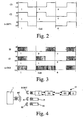
- the second signal-mixing means 5 are arranged to mix the communication-stage output signals C3 and C2 received, i.e. to superimpose them on one another bit by bit, as shown in the signal diagram in Fig. 2 .
- the signal waveforms in the signal diagram show three bits of items of identifying information UID3 and UID2 respectively, which bits are coded in the Manchester code.
- the Manchester code requires that a change of level take place every half bit-length, or in other words, if the bit concerned is a logic 1 that a change take place from a high level HI to a low level LO, and if the bit concerned is a logic 0, that a change take place from a low level LO to a high level HI.
- the communication-stage output signal C3 has the bit sequence 1-0-0 and the communication-stage output signal C2 has the bit sequence 1-1-0.
- the first bit of the resulting first signal-mixing-means output signal S-OUT1 is a logic one and the third bit is a logic zero, which correspond to the bit values in the communication-stage output signals C3 and C2, whereas there is a data collision Coll at the third bit because the values of the communication-stage output signals C3 and C2 are different at this bit position and the signal waveform resulting from the OR gating is at the high level HI throughout the bit, which constitutes what is termed a code violation in the case of the Manchester code.
- the signal-mixing means 5 are therefore arranged to emit a collision signal representing the result of the mixing, which collision signal represents a simultaneous occurrence in an electrical field of two communication-stage output signals C3 and C2 that differ in respect of the information they contain in one unit of information.
- a collision signal representing the result of the mixing
- the collision signal represents a simultaneous occurrence in an electrical field of two communication-stage output signals C3 and C2 that differ in respect of the information they contain in one unit of information.
- Fig. 3 In the first signal waveform El is shown schematically the load modulation of a carrier signal by the communication-stage output signal C3 alone. In the second signal waveform is shown schematically the load modulation of the carrier signal by the communication-stage output signal C2 alone.
- the third signal waveform is shown, at a signal segment Coll, a mixture of the modulations of the carrier signal that are caused by the two communication-stage output signals C3 and C2, such as would be caused by the signal segment Coll shown in Fig. 2 if the signal waveform shown at that point in the first signal-mixing-means output signal S-OUT1 were used to load-modulate the carrier signal.
- the first signal-mixing means output signal S-OUT1 can be passed on by means of the first interface means of the data carrier DC to the communications-device circuit 2 and can be fed there to the first signal-mixing means 5.
- the first communication-stage output signal C1 is mixed, bit-by-bit likewise, with the first signal-mixing-means output signal S-OUT1 that represents the communication-stage output signals C2 and C3 that have already been mixed previously, as a result of which a second signal-mixing-means output signal S-OUT2 is obtained, which is transmitted to the interface means CIU. Because each of the communication-stage output signals C1, C2 and C3 is individual, the second signal-mixing-means output signal S-OUT2 has at least two signal segments Coll in the present case, although this has not been specifically shown in graphic form.
- bits of the two communication-stage output signals C3 and C2 that correspond to one another are mixed with one another at the second mixing means 5 and the mixed signal represented by the first signal-mixing-means output signal S-OUT1 is transmitted without delay to the first signal-mixing means 5 and the bit of the first communication-stage output signal C1 that corresponds in respect of its bit position is mixed in.
- the advantage is obtained that the collision at a bit position in the response to the inventorizing command that is transmitted by means of the transmission means 10 is detected at a conventional read/write station 1, even though this collision did not occur in the electromagnetic field between the read/write station 1 and the communications device 13 and instead was produced by means of the first or second signal-mixing means 5, and the read/write station 1 is then able to work through a conventional anti-collision protocol of the kind for which provision is made in standard ISO 14443.
- NFC devices near-field communication devices
- the communications device that is active in respect of communication in this case is the one that was either selected to communicate by selection as part of an anti-collision procedure, in the way that is usual for data carriers or their circuits conforming to standard ISO 14444 or for NFC devices, either of which are being operated in their passive communications mode. This is also of importance in the case of an NFC device that has became active as part of a so-called collision avoidance procedure under ISO 18092.
- the priority-ensuring means may for example cooperate with the individual communication stages 6, 8 and 9 and monitor the activities or states of the latter and, as soon as a state that is active in respect of communication is detected at one of the communication stages, may act on the states of the other communication stages to the effect that these remain in their state that is inactive in respect of communication, i.e. do not make any unwanted use of the shared transmission means 10 or the shared interface CIU.
- the priority-ensuring means are produced by means of software.
- the conventional read/write station 1 is shown opposite two conventional contactless data carriers 15, 16 and the communications device 13 according to the invention, the communications device 13 having a communications-device circuit 2 according to the invention, cascaded data carriers DC according to the invention each with a data-carrier circuit 3 according to the invention, and a conventional data carrier 4.
- the data carriers DC and 4 may each be configured to have CPUs of their own and thus to have a certain intelligence of their own. In a configuration of this kind, applications with secure data storage are also possible.
- the read/write station 1 transmits an inventorizing command that can be transmitted by means of the electromagnetic signal ES, the conventional contactless data carriers 15, 16 and the communication stages contained in the communications device 13, which are not explicitly shown, respond by announcing their specific items of identifying information.
- collisions may occur at different bit positions in the items of identifying information communicated to the read/write station 1, it being immaterial whether these collisions are produced in the electromagnetic field by the communications device 13 and the data carriers 14 and 15 or in the communications device 13 by means of the signal-mixing means 5 contained in the communications-device circuit 2 or the data-carrier circuit 3.
- the read-write station 1 is able to perform a conventional anti-collision procedure in order to determine the items of identifying information of all the data carriers DC or 4 situated in its communications zone, or to be more exact of all the communication stages that are present, and in this way to select, separately, the data carriers 15,16, the communications-device circuit 2, one of the cascaded data carriers DC according to the invention, or the cascaded conventional data carrier 4, and thus to address them selectively.
- the communication stages of the circuits 2 and 3 may, as well as having the functionality of the signal-mixing means, also perform the function of known data carriers, such as that of a smart card, conforming to for example standard ISO 14443, or that of a dual interface card, such for example as one conforming to the de facto MIFARE® standard, or that of an SIM (subscriber identity module) for mobile telephones, or combined functions.
- known data carriers such as that of a smart card, conforming to for example standard ISO 14443, or that of a dual interface card, such for example as one conforming to the de facto MIFARE® standard, or that of an SIM (subscriber identity module) for mobile telephones, or combined functions.
- the communication stages of the circuits 2 and 3 according to the invention may perform the function ofNFC devices, conforming to standard ISO 18092 for example.
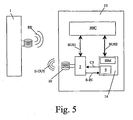
- Fig. 5 shows a communications device 13 in the form of a mobile telephone having, incorporated in the mobile telephone, a communications-device circuit 2 according to the invention that is able to receive, via the transmission means 10, electromagnetic signals ES from the read-write station 1 external to the mobile telephone and is itself able to transmit electromagnetic signals E-OUT to the read/write station 1.
- the circuit 2 is cascaded, in the manner according to the invention, by contacts with a conventional data carrier 4 that is able to be removed from the mobile telephone.
- the circuit 2 is of the type that was described by reference to Fig.
- the data carrier 4 has a common substrate 14 for, firstly, a subscriber identity module (SIM) that is required for the operation of the mobile telephone and is connected via a data-bus BUS2 that operates to standard ISO 7816 to a baseband controller BBC that controls essential functions of the mobile telephone and, secondly, a secure application module (SAM) by which secure applications are implemented.
- SIM subscriber identity module
- SAM secure application module
- the baseband controller BBC is also connected in this case to the circuit 2 according to the invention, via a serial data-bus BUS1.
- the communications device 13 according to the invention can be used for a large number of applications. Examples of applications of this kind that may be mentioned are the on-line booking of tickets, or the loading of the communications device 13, via an external read/write station, with authorizing information that can be read by access systems, as a result of which the communications device can act as an electronic "key".
- the implementation of electronic purses or a credit card is possible in a similar way.
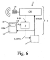
- the communications device 13 shown in Fig. 6 is arranged to mix communication-stage output signals C1 to C4 at the reception end.
- the communications device 13 shown in Fig. 6 acts as a read/write station according to the invention that is arranged for contactless communication under standard ISO 14443 and, in a similar way to the communications device 13 shown in Fig. 1 , it has the communications-device circuit 2 according to the invention, the signal-mixing means 5 being provided in the present case downstream of the interface means CIU in a reception branch.
- the signal-mixing means 5 are suitable for receiving the input signal S-IN emitted by the interface means CIU, which signal S-IN represents, in the present case, a response from a partner communications device that is communicating with the communications device 13.
- a partner communications device of this kind is formed in the present case by the communications device 13 shown in Fig.
- each of the conventional data carriers 15 and 16 shown in Fig. 4 may equally well form the partner communications device, the items of identifying information from these data carriers being mixed in the electromagnetic field.
- a fourth communication stage 17 that is arranged to generate the inventorizing command and to transmit the inventorizing command in the form of third communication-stage output signals S-OUT3 to the interface means CIU, by means of which the signals are communicated to the partner communications device.
- a conventional data carrier 18 that provides the function of what is termed a secure application module (SAM) and that has a fourth communication stage 18', which latter can be uniquely identified by a fourth item of identifying information UID4 that is stored in it.
- SAM secure application module
- the data carrier 18 is coupled to the communication stage 17 in such a way that the third communication-stage output signal S-OUT3 can be fed to it by contact means, by means of which signal it too can be requested to transmit its item of identifying information UID4 to the signal-mixing means 5, where the fourth item of identifying information UID4 is mixed either with a single other communication-stage output signal C1, C2 or C3 that has been received via the electromagnetic field, or with already premixed communication-stage output signals C1, C2 and C3 that have been received via the electromagnetic field.
- the signal-mixing means 5 are connected to the fourth communication stage 17 and they are arranged to emit a signal-mixing-means output signal S-OUT4 that represents the mixing of at least two of the communication-stage output signals C1, C2, C3 and C4.
- a signal-mixing-means output signal S-OUT4 that represents the mixing of at least two of the communication-stage output signals C1, C2, C3 and C4.
- the communication stage 17 As soon as the communication stage 17 detects a collision at a bit position in the signal-mixing-means output signal S-OUT4, it starts an anti-collision procedure under standard ISO 14443, in which the commands and parameters that the communication stage 17 is able to emit in this case are communicated with the help of the communication-stage output signal S-OUT3 both to the external communication stages and to the internal communication stage of the data carrier 18.
- the input signal may also be fed to the interface means CIU from within the communications device or from outside the communications device, as desired.
- the second signal-mixing-means output signal S-OUT2 may also be made available for internal processing within the communications device 13.
Landscapes
- Engineering & Computer Science (AREA)
- Artificial Intelligence (AREA)
- Computer Vision & Pattern Recognition (AREA)
- Physics & Mathematics (AREA)
- General Physics & Mathematics (AREA)
- Theoretical Computer Science (AREA)
- Near-Field Transmission Systems (AREA)
- Electrophonic Musical Instruments (AREA)
- Input Circuits Of Receivers And Coupling Of Receivers And Audio Equipment (AREA)
- Channel Selection Circuits, Automatic Tuning Circuits (AREA)
Claims (8)
- Schaltung (2, 3) zum Verarbeiten von wenigstens zwei Ausgangssignalen (C1, C2, C3), umfassend:Signalmischmittel (5), die so ausgeführt sind, dass sie wenigstens zwei Ausgangssignale (C1, C2, C3) von Kommunikationsstufen empfangen, um die wenigstens zwei Ausgangssignale (C1, C2, C3) durch Überlagerung derselben zu mischen, und ein Kollisionssignal emittieren, das das Ergebnis des Mischens der wenigstens zwei Ausgangssignale (C1, C2, C3) repräsentiert, wobei das Kollisionssignal eine Überlagerung der wenigstens zwei Ausgangssignale (C1, C2, C3) ist, die ein gleichzeitiges Auftreten der wenigstens zwei Ausgangssignale (C1, C2, C3) in einem elektromagnetischen Feld repräsentiert.
- Schaltung (2, 3) nach Anspruch 1, wobei die Signalmischmittel (5) so ausgeführt sind, dass sie die wenigstens zwei Ausgangssignale (C1, C2, C3) der Kommunikationsstufen, die empfangen werden, in Bezug auf die Einheiten der Informationen, die jeweils durch diese repräsentiert werden und die einander entsprechen, logisch verarbeiten.
- Schaltung (2, 3) nach Anspruch 2, wobei die Signalmischmittel (5) so ausgeführt sind, dass sie ein Ausgangssignal (C1, C2, C3) einer Kommunikationsstufe verarbeiten, das im Manchester-Code codiert ist.
- Schaltung (2, 3) nach irgendeinem der Ansprüche 1, 2 oder 3, wobei die Schaltung (2, 3) Prioritätssicherstellungsmittel aufweist, die so beschaffen sind, dass sie, sobald wenigstens eine der Kommunikationsstufen aktiviert worden ist, um zu kommunizieren, sicherstellen, dass diese wenigstens eine ausgewählte Kommunikationsstufe ihre Priorität in Bezug auf die Kommunikation über einer weiteren Kommunikationsstufe, die nicht ausgewählt worden ist, beibehält.
- Datenträger (DC), der eine Schaltung aufweist, wobei der Datenträger (DC) mit einer Schaltung nach irgendeinem der Ansprüche 1 bis 4 versehen ist, wobei die Schaltung (3) Schnittstellenmittel aufweist, die für eine Kommunikation mittels Kontakt und/oder für eine kontaktlose Kommunikation ausgelegt sind, wobei die Schaltung (3) eine Kommunikationsstufe (8) aufweist, die so ausgeführt ist, dass sie ein Ausgangssignal (C1, C2, C3) der Kommunikationsstufe erzeugt und emittiert, und wobei die Signalmischmittel (5) so ausgeführt sind, dass sie mit der Kommunikationsstufe (8) kooperieren und mit den Schnittstellenmitteln kooperieren.
- Kommunikationsvorrichtung (13), die eine Schaltung aufweist, wobei die Kommunikationsvorrichtung (13) mit wenigstens einer Schaltung (2) nach irgendeinem der Ansprüche 1 bis 4 und/oder mit wenigstens einem Datenträger (DC) nach Anspruch 5 versehen ist.
- Kommunikationsvorrichtung (13) nach Anspruch 6, wobei die Kommunikationsvorrichtung (13) die Form eines Mobiltelephons oder eines persönlichen digitalen Assistenten (PDA) aufweist.
- Kommunikationsvorrichtung (13) nach Anspruch 6, wobei die Kommunikationsvorrichtung (13) die Form einer Lese/Schreib-Station für Datenträger (DC, 4,15,16) aufweist.
Priority Applications (1)
| Application Number | Priority Date | Filing Date | Title |
|---|---|---|---|
| EP05718767A EP1745404B1 (de) | 2004-04-29 | 2005-04-20 | Schaltung zum verarbeiten von ausgangssignalen von kommunikationsstufen |
Applications Claiming Priority (3)
| Application Number | Priority Date | Filing Date | Title |
|---|---|---|---|
| EP04101839 | 2004-04-29 | ||
| EP05718767A EP1745404B1 (de) | 2004-04-29 | 2005-04-20 | Schaltung zum verarbeiten von ausgangssignalen von kommunikationsstufen |
| PCT/IB2005/051288 WO2005106766A1 (en) | 2004-04-29 | 2005-04-20 | Circuit for processing an output signal of a communication stage |
Publications (2)
| Publication Number | Publication Date |
|---|---|
| EP1745404A1 EP1745404A1 (de) | 2007-01-24 |
| EP1745404B1 true EP1745404B1 (de) | 2010-03-24 |
Family
ID=34965423
Family Applications (1)
| Application Number | Title | Priority Date | Filing Date |
|---|---|---|---|
| EP05718767A Ceased EP1745404B1 (de) | 2004-04-29 | 2005-04-20 | Schaltung zum verarbeiten von ausgangssignalen von kommunikationsstufen |
Country Status (6)
| Country | Link |
|---|---|
| EP (1) | EP1745404B1 (de) |
| JP (1) | JP4796054B2 (de) |
| CN (1) | CN1957358B (de) |
| AT (1) | ATE462167T1 (de) |
| DE (1) | DE602005020128D1 (de) |
| WO (1) | WO2005106766A1 (de) |
Families Citing this family (3)
| Publication number | Priority date | Publication date | Assignee | Title |
|---|---|---|---|---|
| JP4224080B2 (ja) | 2006-06-05 | 2009-02-12 | フェリカネットワークス株式会社 | 情報処理端末およびそのプログラム |
| JP2016508749A (ja) * | 2012-12-14 | 2016-03-24 | リナック エー/エス | 電動アクチュエータシステム |
| US9471523B2 (en) * | 2013-09-18 | 2016-10-18 | Infineon Technologies Ag | Serial interface systems and methods having multiple modes of serial communication |
Family Cites Families (6)
| Publication number | Priority date | Publication date | Assignee | Title |
|---|---|---|---|---|
| JP3122682B2 (ja) * | 1991-12-04 | 2001-01-09 | 東芝キヤリア株式会社 | データ送受信装置 |
| GB2269512B (en) * | 1992-08-03 | 1996-08-14 | Nokia Mobile Phones Uk | Radio arrangement |
| US6185436B1 (en) * | 1997-03-27 | 2001-02-06 | Siemens Information And Communication Networks, Inc. | Wireless communication system |
| EP1051052A1 (de) * | 1999-05-07 | 2000-11-08 | Darwish Bin Karam Humaid | Funktelefon mit mehrere SIM Kartleser |
| JP2003189361A (ja) * | 2001-12-18 | 2003-07-04 | Toshiba Corp | 移動通信端末 |
| US20050099267A1 (en) * | 2002-03-13 | 2005-05-12 | Franz Amtmann | Communication station for communication with transponders and further communication stations with the aid of different transmission parameters |
-
2005
- 2005-04-20 WO PCT/IB2005/051288 patent/WO2005106766A1/en not_active Ceased
- 2005-04-20 JP JP2007510183A patent/JP4796054B2/ja not_active Expired - Fee Related
- 2005-04-20 DE DE602005020128T patent/DE602005020128D1/de not_active Expired - Lifetime
- 2005-04-20 CN CN2005800133360A patent/CN1957358B/zh not_active Expired - Fee Related
- 2005-04-20 AT AT05718767T patent/ATE462167T1/de not_active IP Right Cessation
- 2005-04-20 EP EP05718767A patent/EP1745404B1/de not_active Ceased
Also Published As
| Publication number | Publication date |
|---|---|
| CN1957358A (zh) | 2007-05-02 |
| WO2005106766A1 (en) | 2005-11-10 |
| CN1957358B (zh) | 2010-06-23 |
| JP2007535059A (ja) | 2007-11-29 |
| DE602005020128D1 (de) | 2010-05-06 |
| EP1745404A1 (de) | 2007-01-24 |
| JP4796054B2 (ja) | 2011-10-19 |
| ATE462167T1 (de) | 2010-04-15 |
Similar Documents
| Publication | Publication Date | Title |
|---|---|---|
| US7941176B2 (en) | Circuit for processing an output signal of a communication stage | |
| JP5621038B2 (ja) | Nfcコントローラを用いた通信の管理方法 | |
| EP4058925B1 (de) | Systeme und verfahren zur übersetzung von drahtlosgerätesignalen | |
| EP2485407B1 (de) | Koordination mehrerer kontaktloser Datenträger | |
| EP2809054B1 (de) | Mobile elektronische Vorrichtung mit Sender-Empfänger für drahtlosen Datenaustausch | |
| KR101210000B1 (ko) | 마이크로프로세서 카드 | |
| US20090152361A1 (en) | Memory card based contactless devices | |
| DE69822184D1 (de) | System zur automatischen kontaktlosen datensammlung | |
| US20080048036A1 (en) | Contactless Ic Chip Reader/Writer | |
| EP1675034B1 (de) | Übertragungs- und Empfangsvorrichtung sowie Übertragungs- und Empfangsverfahren | |
| EP1895449B1 (de) | Datenkommunikationssystem, einrichtung zur ausführung einer chipkartenfunktion, steuerverfahren für die einrichtung und informationsverarbeitungsendgerät | |
| CN101561861B (zh) | 在具有中央和外围电路的便携智能物体中的电感耦合交换 | |
| EP0939935B1 (de) | Hybrid-datenträger und schaltung mit potentialausgleichsvorrichtung zur egalisierung der potentiale auf wenigstens zwei kontaktelementen | |
| EP1745404B1 (de) | Schaltung zum verarbeiten von ausgangssignalen von kommunikationsstufen | |
| JP4284745B2 (ja) | Icカード通信システム | |
| EP2782400A1 (de) | NFC-Steuerungsarchitektur zur simultanen Emulation mehrerer NFC-Technologien in einer NFC-Hörvorrichtung | |
| CN118659803B (zh) | 近场通信方法及装置 | |
| CN105872955A (zh) | 整合近场通信的触控集成电路及其近场通信方法 | |
| EP0907137B1 (de) | System und Verfahren zum Verarbeiten von Chipkarten | |
| US20260127403A1 (en) | Dual communication frequency rfid circuit | |
| JP7386221B2 (ja) | アンテナデバイス及び関連する通信方法 | |
| HK40079457A (en) | Antenna device and related communication method | |
| CN102567776A (zh) | 一种可快速进行模式选择的双界面智能卡和实现方法 | |
| JP4736197B2 (ja) | リーダライタ | |
| CN1996337A (zh) | 集成rfid和rfid读写器的终端设备 |
Legal Events
| Date | Code | Title | Description |
|---|---|---|---|
| PUAI | Public reference made under article 153(3) epc to a published international application that has entered the european phase |
Free format text: ORIGINAL CODE: 0009012 |
|
| 17P | Request for examination filed |
Effective date: 20061129 |
|
| AK | Designated contracting states |
Kind code of ref document: A1 Designated state(s): AT BE BG CH CY CZ DE DK EE ES FI FR GB GR HU IE IS IT LI LT LU MC NL PL PT RO SE SI SK TR |
|
| RAP1 | Party data changed (applicant data changed or rights of an application transferred) |
Owner name: NXP B.V. |
|
| DAX | Request for extension of the european patent (deleted) | ||
| 17Q | First examination report despatched |
Effective date: 20081002 |
|
| RTI1 | Title (correction) |
Free format text: CIRCUIT FOR PROCESSING OUTPUT SIGNALS OF COMMUNICATION STAGES |
|
| GRAP | Despatch of communication of intention to grant a patent |
Free format text: ORIGINAL CODE: EPIDOSNIGR1 |
|
| GRAS | Grant fee paid |
Free format text: ORIGINAL CODE: EPIDOSNIGR3 |
|
| GRAA | (expected) grant |
Free format text: ORIGINAL CODE: 0009210 |
|
| AK | Designated contracting states |
Kind code of ref document: B1 Designated state(s): AT BE BG CH CY CZ DE DK EE ES FI FR GB GR HU IE IS IT LI LT LU MC NL PL PT RO SE SI SK TR |
|
| REG | Reference to a national code |
Ref country code: GB Ref legal event code: FG4D |
|
| REG | Reference to a national code |
Ref country code: CH Ref legal event code: EP |
|
| REG | Reference to a national code |
Ref country code: IE Ref legal event code: FG4D |
|
| REF | Corresponds to: |
Ref document number: 602005020128 Country of ref document: DE Date of ref document: 20100506 Kind code of ref document: P |
|
| REG | Reference to a national code |
Ref country code: NL Ref legal event code: VDEP Effective date: 20100324 |
|
| PG25 | Lapsed in a contracting state [announced via postgrant information from national office to epo] |
Ref country code: LT Free format text: LAPSE BECAUSE OF FAILURE TO SUBMIT A TRANSLATION OF THE DESCRIPTION OR TO PAY THE FEE WITHIN THE PRESCRIBED TIME-LIMIT Effective date: 20100324 |
|
| LTIE | Lt: invalidation of european patent or patent extension |
Effective date: 20100324 |
|
| PG25 | Lapsed in a contracting state [announced via postgrant information from national office to epo] |
Ref country code: PL Free format text: LAPSE BECAUSE OF FAILURE TO SUBMIT A TRANSLATION OF THE DESCRIPTION OR TO PAY THE FEE WITHIN THE PRESCRIBED TIME-LIMIT Effective date: 20100324 Ref country code: SI Free format text: LAPSE BECAUSE OF FAILURE TO SUBMIT A TRANSLATION OF THE DESCRIPTION OR TO PAY THE FEE WITHIN THE PRESCRIBED TIME-LIMIT Effective date: 20100324 Ref country code: AT Free format text: LAPSE BECAUSE OF FAILURE TO SUBMIT A TRANSLATION OF THE DESCRIPTION OR TO PAY THE FEE WITHIN THE PRESCRIBED TIME-LIMIT Effective date: 20100324 Ref country code: FI Free format text: LAPSE BECAUSE OF FAILURE TO SUBMIT A TRANSLATION OF THE DESCRIPTION OR TO PAY THE FEE WITHIN THE PRESCRIBED TIME-LIMIT Effective date: 20100324 |
|
| PG25 | Lapsed in a contracting state [announced via postgrant information from national office to epo] |
Ref country code: EE Free format text: LAPSE BECAUSE OF FAILURE TO SUBMIT A TRANSLATION OF THE DESCRIPTION OR TO PAY THE FEE WITHIN THE PRESCRIBED TIME-LIMIT Effective date: 20100324 Ref country code: SE Free format text: LAPSE BECAUSE OF FAILURE TO SUBMIT A TRANSLATION OF THE DESCRIPTION OR TO PAY THE FEE WITHIN THE PRESCRIBED TIME-LIMIT Effective date: 20100324 Ref country code: GR Free format text: LAPSE BECAUSE OF FAILURE TO SUBMIT A TRANSLATION OF THE DESCRIPTION OR TO PAY THE FEE WITHIN THE PRESCRIBED TIME-LIMIT Effective date: 20100625 Ref country code: ES Free format text: LAPSE BECAUSE OF FAILURE TO SUBMIT A TRANSLATION OF THE DESCRIPTION OR TO PAY THE FEE WITHIN THE PRESCRIBED TIME-LIMIT Effective date: 20100705 Ref country code: BE Free format text: LAPSE BECAUSE OF FAILURE TO SUBMIT A TRANSLATION OF THE DESCRIPTION OR TO PAY THE FEE WITHIN THE PRESCRIBED TIME-LIMIT Effective date: 20100324 Ref country code: RO Free format text: LAPSE BECAUSE OF FAILURE TO SUBMIT A TRANSLATION OF THE DESCRIPTION OR TO PAY THE FEE WITHIN THE PRESCRIBED TIME-LIMIT Effective date: 20100324 Ref country code: NL Free format text: LAPSE BECAUSE OF FAILURE TO SUBMIT A TRANSLATION OF THE DESCRIPTION OR TO PAY THE FEE WITHIN THE PRESCRIBED TIME-LIMIT Effective date: 20100324 |
|
| PG25 | Lapsed in a contracting state [announced via postgrant information from national office to epo] |
Ref country code: MC Free format text: LAPSE BECAUSE OF NON-PAYMENT OF DUE FEES Effective date: 20100430 Ref country code: CZ Free format text: LAPSE BECAUSE OF FAILURE TO SUBMIT A TRANSLATION OF THE DESCRIPTION OR TO PAY THE FEE WITHIN THE PRESCRIBED TIME-LIMIT Effective date: 20100324 Ref country code: SK Free format text: LAPSE BECAUSE OF FAILURE TO SUBMIT A TRANSLATION OF THE DESCRIPTION OR TO PAY THE FEE WITHIN THE PRESCRIBED TIME-LIMIT Effective date: 20100324 Ref country code: IS Free format text: LAPSE BECAUSE OF FAILURE TO SUBMIT A TRANSLATION OF THE DESCRIPTION OR TO PAY THE FEE WITHIN THE PRESCRIBED TIME-LIMIT Effective date: 20100724 Ref country code: BG Free format text: LAPSE BECAUSE OF FAILURE TO SUBMIT A TRANSLATION OF THE DESCRIPTION OR TO PAY THE FEE WITHIN THE PRESCRIBED TIME-LIMIT Effective date: 20100624 |
|
| REG | Reference to a national code |
Ref country code: CH Ref legal event code: PL |
|
| PLBE | No opposition filed within time limit |
Free format text: ORIGINAL CODE: 0009261 |
|
| STAA | Information on the status of an ep patent application or granted ep patent |
Free format text: STATUS: NO OPPOSITION FILED WITHIN TIME LIMIT |
|
| PG25 | Lapsed in a contracting state [announced via postgrant information from national office to epo] |
Ref country code: PT Free format text: LAPSE BECAUSE OF FAILURE TO SUBMIT A TRANSLATION OF THE DESCRIPTION OR TO PAY THE FEE WITHIN THE PRESCRIBED TIME-LIMIT Effective date: 20100726 Ref country code: DK Free format text: LAPSE BECAUSE OF FAILURE TO SUBMIT A TRANSLATION OF THE DESCRIPTION OR TO PAY THE FEE WITHIN THE PRESCRIBED TIME-LIMIT Effective date: 20100324 Ref country code: IE Free format text: LAPSE BECAUSE OF NON-PAYMENT OF DUE FEES Effective date: 20100420 |
|
| PG25 | Lapsed in a contracting state [announced via postgrant information from national office to epo] |
Ref country code: CH Free format text: LAPSE BECAUSE OF NON-PAYMENT OF DUE FEES Effective date: 20100430 Ref country code: LI Free format text: LAPSE BECAUSE OF NON-PAYMENT OF DUE FEES Effective date: 20100430 |
|
| 26N | No opposition filed |
Effective date: 20101228 |
|
| PG25 | Lapsed in a contracting state [announced via postgrant information from national office to epo] |
Ref country code: IT Free format text: LAPSE BECAUSE OF FAILURE TO SUBMIT A TRANSLATION OF THE DESCRIPTION OR TO PAY THE FEE WITHIN THE PRESCRIBED TIME-LIMIT Effective date: 20100324 |
|
| REG | Reference to a national code |
Ref country code: GB Ref legal event code: 732E Free format text: REGISTERED BETWEEN 20120621 AND 20120627 |
|
| REG | Reference to a national code |
Ref country code: GB Ref legal event code: 732E Free format text: REGISTERED BETWEEN 20120705 AND 20120711 |
|
| PG25 | Lapsed in a contracting state [announced via postgrant information from national office to epo] |
Ref country code: CY Free format text: LAPSE BECAUSE OF FAILURE TO SUBMIT A TRANSLATION OF THE DESCRIPTION OR TO PAY THE FEE WITHIN THE PRESCRIBED TIME-LIMIT Effective date: 20100324 |
|
| PG25 | Lapsed in a contracting state [announced via postgrant information from national office to epo] |
Ref country code: HU Free format text: LAPSE BECAUSE OF FAILURE TO SUBMIT A TRANSLATION OF THE DESCRIPTION OR TO PAY THE FEE WITHIN THE PRESCRIBED TIME-LIMIT Effective date: 20100925 Ref country code: LU Free format text: LAPSE BECAUSE OF NON-PAYMENT OF DUE FEES Effective date: 20100420 |
|
| REG | Reference to a national code |
Ref country code: GB Ref legal event code: 732E Free format text: REGISTERED BETWEEN 20120927 AND 20121003 |
|
| PG25 | Lapsed in a contracting state [announced via postgrant information from national office to epo] |
Ref country code: TR Free format text: LAPSE BECAUSE OF FAILURE TO SUBMIT A TRANSLATION OF THE DESCRIPTION OR TO PAY THE FEE WITHIN THE PRESCRIBED TIME-LIMIT Effective date: 20100324 |
|
| REG | Reference to a national code |
Ref country code: GB Ref legal event code: 732E Free format text: REGISTERED BETWEEN 20130606 AND 20130612 |
|
| REG | Reference to a national code |
Ref country code: GB Ref legal event code: 732E Free format text: REGISTERED BETWEEN 20140619 AND 20140625 |
|
| REG | Reference to a national code |
Ref country code: FR Ref legal event code: TP Owner name: QUOTAINNE ENTERPRISES LLC, US Effective date: 20141224 |
|
| REG | Reference to a national code |
Ref country code: DE Ref legal event code: R081 Ref document number: 602005020128 Country of ref document: DE Owner name: QUOTAINNE ENTERPRISES LLC, WILMINGTON, US Free format text: FORMER OWNER: NXP B.V., EINDHOVEN, NL Effective date: 20150113 |
|
| REG | Reference to a national code |
Ref country code: FR Ref legal event code: PLFP Year of fee payment: 12 |
|
| REG | Reference to a national code |
Ref country code: FR Ref legal event code: PLFP Year of fee payment: 13 |
|
| REG | Reference to a national code |
Ref country code: FR Ref legal event code: PLFP Year of fee payment: 14 |
|
| PGFP | Annual fee paid to national office [announced via postgrant information from national office to epo] |
Ref country code: FR Payment date: 20230309 Year of fee payment: 19 |
|
| PGFP | Annual fee paid to national office [announced via postgrant information from national office to epo] |
Ref country code: GB Payment date: 20230302 Year of fee payment: 19 |
|
| PGFP | Annual fee paid to national office [announced via postgrant information from national office to epo] |
Ref country code: DE Payment date: 20230307 Year of fee payment: 19 |
|
| REG | Reference to a national code |
Ref country code: DE Ref legal event code: R119 Ref document number: 602005020128 Country of ref document: DE |
|
| GBPC | Gb: european patent ceased through non-payment of renewal fee |
Effective date: 20240420 |
|
| PG25 | Lapsed in a contracting state [announced via postgrant information from national office to epo] |
Ref country code: DE Free format text: LAPSE BECAUSE OF NON-PAYMENT OF DUE FEES Effective date: 20241105 |
|
| PG25 | Lapsed in a contracting state [announced via postgrant information from national office to epo] |
Ref country code: GB Free format text: LAPSE BECAUSE OF NON-PAYMENT OF DUE FEES Effective date: 20240420 |
|
| PG25 | Lapsed in a contracting state [announced via postgrant information from national office to epo] |
Ref country code: FR Free format text: LAPSE BECAUSE OF NON-PAYMENT OF DUE FEES Effective date: 20240430 |
|
| PG25 | Lapsed in a contracting state [announced via postgrant information from national office to epo] |
Ref country code: GB Free format text: LAPSE BECAUSE OF NON-PAYMENT OF DUE FEES Effective date: 20240420 Ref country code: FR Free format text: LAPSE BECAUSE OF NON-PAYMENT OF DUE FEES Effective date: 20240430 Ref country code: DE Free format text: LAPSE BECAUSE OF NON-PAYMENT OF DUE FEES Effective date: 20241105 |