EP1746485A2 - Verfahren zur Integration eines Digitalisiereingabegeräts in eine Anzeige - Google Patents
Verfahren zur Integration eines Digitalisiereingabegeräts in eine Anzeige Download PDFInfo
- Publication number
- EP1746485A2 EP1746485A2 EP06117673A EP06117673A EP1746485A2 EP 1746485 A2 EP1746485 A2 EP 1746485A2 EP 06117673 A EP06117673 A EP 06117673A EP 06117673 A EP06117673 A EP 06117673A EP 1746485 A2 EP1746485 A2 EP 1746485A2
- Authority
- EP
- European Patent Office
- Prior art keywords
- digitizer
- substrate
- display element
- display
- layer
- Prior art date
- Legal status (The legal status is an assumption and is not a legal conclusion. Google has not performed a legal analysis and makes no representation as to the accuracy of the status listed.)
- Withdrawn
Links
Images




Classifications
-
- G—PHYSICS
- G06—COMPUTING OR CALCULATING; COUNTING
- G06F—ELECTRIC DIGITAL DATA PROCESSING
- G06F3/00—Input arrangements for transferring data to be processed into a form capable of being handled by the computer; Output arrangements for transferring data from processing unit to output unit, e.g. interface arrangements
- G06F3/01—Input arrangements or combined input and output arrangements for interaction between user and computer
- G06F3/03—Arrangements for converting the position or the displacement of a member into a coded form
- G06F3/041—Digitisers, e.g. for touch screens or touch pads, characterised by the transducing means
- G06F3/0412—Digitisers structurally integrated in a display
-
- G—PHYSICS
- G02—OPTICS
- G02F—OPTICAL DEVICES OR ARRANGEMENTS FOR THE CONTROL OF LIGHT BY MODIFICATION OF THE OPTICAL PROPERTIES OF THE MEDIA OF THE ELEMENTS INVOLVED THEREIN; NON-LINEAR OPTICS; FREQUENCY-CHANGING OF LIGHT; OPTICAL LOGIC ELEMENTS; OPTICAL ANALOGUE/DIGITAL CONVERTERS
- G02F1/00—Devices or arrangements for the control of the intensity, colour, phase, polarisation or direction of light arriving from an independent light source, e.g. switching, gating or modulating; Non-linear optics
- G02F1/01—Devices or arrangements for the control of the intensity, colour, phase, polarisation or direction of light arriving from an independent light source, e.g. switching, gating or modulating; Non-linear optics for the control of the intensity, phase, polarisation or colour
- G02F1/13—Devices or arrangements for the control of the intensity, colour, phase, polarisation or direction of light arriving from an independent light source, e.g. switching, gating or modulating; Non-linear optics for the control of the intensity, phase, polarisation or colour based on liquid crystals, e.g. single liquid crystal display cells
- G02F1/133—Constructional arrangements; Operation of liquid crystal cells; Circuit arrangements
- G02F1/1333—Constructional arrangements; Manufacturing methods
- G02F1/13338—Input devices, e.g. touch panels
-
- G—PHYSICS
- G02—OPTICS
- G02F—OPTICAL DEVICES OR ARRANGEMENTS FOR THE CONTROL OF LIGHT BY MODIFICATION OF THE OPTICAL PROPERTIES OF THE MEDIA OF THE ELEMENTS INVOLVED THEREIN; NON-LINEAR OPTICS; FREQUENCY-CHANGING OF LIGHT; OPTICAL LOGIC ELEMENTS; OPTICAL ANALOGUE/DIGITAL CONVERTERS
- G02F1/00—Devices or arrangements for the control of the intensity, colour, phase, polarisation or direction of light arriving from an independent light source, e.g. switching, gating or modulating; Non-linear optics
- G02F1/01—Devices or arrangements for the control of the intensity, colour, phase, polarisation or direction of light arriving from an independent light source, e.g. switching, gating or modulating; Non-linear optics for the control of the intensity, phase, polarisation or colour
- G02F1/13—Devices or arrangements for the control of the intensity, colour, phase, polarisation or direction of light arriving from an independent light source, e.g. switching, gating or modulating; Non-linear optics for the control of the intensity, phase, polarisation or colour based on liquid crystals, e.g. single liquid crystal display cells
- G02F1/133—Constructional arrangements; Operation of liquid crystal cells; Circuit arrangements
- G02F1/1333—Constructional arrangements; Manufacturing methods
- G02F1/1335—Structural association of cells with optical devices, e.g. polarisers or reflectors
- G02F1/13356—Structural association of cells with optical devices, e.g. polarisers or reflectors characterised by the placement of the optical elements
- G02F1/133565—Structural association of cells with optical devices, e.g. polarisers or reflectors characterised by the placement of the optical elements inside the LC elements, i.e. between the cell substrates
-
- G—PHYSICS
- G06—COMPUTING OR CALCULATING; COUNTING
- G06F—ELECTRIC DIGITAL DATA PROCESSING
- G06F2203/00—Indexing scheme relating to G06F3/00 - G06F3/048
- G06F2203/041—Indexing scheme relating to G06F3/041 - G06F3/045
- G06F2203/04103—Manufacturing, i.e. details related to manufacturing processes specially suited for touch sensitive devices
Definitions
- the present invention relates generally to flat panel displays, and particularly to a two-dimensional position-detecting digitizer input device for use in flat panel displays, and more particularly to a process for integrating a digitizer input device in a flat panel display.
- LCD liquid crystal displays
- OLED organic light-emitting diode
- One type of LCD is provided with a two-dimensional position-detecting user input device (i.e., a digitizer) to allow user input, such as user interactivity with respect to images displayed (e.g., selecting an icon), handwriting recognition, drawing, cursor control, etc.
- a digitizer i.e., a digitizer
- the digitizer may be based on sensing mechanisms such as resistive sensing, capacitive sensing, infrared sensing, acoustic wave sensing, force sensing, electromagnetic sensing, etc.
- the underlying operational principle is magnetic induction.
- the electromagnetic pen acts as a signal transceiver
- the sensor array acts as a signal receiver
- the controller determines the two-dimensional coordinates of the pen with respect to the sensor array by detecting the current change as a result of magnetic induction in the sensor array caused by a change in magnetic flux brought about by the pen.
- the two-dimensional coordinates of the pen i.e., X-Y coordinates
- Electromagnetic digitizers provide relatively accurate position detection of the pen, in relatively good resolution compared to some of the other forms of sensing mechanisms.
- FIG. 1 schematically illustrates a conventional flat panel display 500 having a flat panel display module 502 (e.g., an LCD module) and a separate electromagnetic digitizer board 504 assembled in a stack.
- the digitizer board 504 is attached to one planar surface of the display module 502.
- a controller 508 is operatively coupled to the digitizer board 504 and a complementary electromagnetic pen 506.
- the digitizer board 504 includes a sensor array, which is formed by conventional printed circuit technology, with sensor array structures fabricated by printing technology.
- Printed circuit technology involves relatively large physical sizes and low resolution, as compared to semiconductor circuit fabrication technology.
- the sensor array includes metal conductive lines with a line width on the order of several hundred micrometers, as compared to semiconductor fabrication technology, involving line width on the order of micrometers. To achieve the desired sensitivity, the physical dimension of the sensor array tends to be relatively bulky. Further, given that the conventional electromagnetic digitizer board 504 is a separate and discrete component attached to the display module 502, it adds to the thickness and weight of the overall flat panel display 500.
- U.S. Patent Application Publication No. US20060146033A1 discloses integrating a digitizer input device into a flat panel display, which reduces the overall thickness and weight of the flat panel display.
- Copending U.S. Patent Application No. filed concurrently herewith (Attorney Docket No. 1131/215), discloses miniaturized digitizer sensor array structures that can be integrated into flat panel display devices.
- the present invention provides improved processes for integrating digitizer sensor array into flat panel displays.
- the sensor array comprises novel sensor segment structures that are particularly suitable for integration into the display module of a display device (e.g., an LCD module of an LCD device or an OLED module of an OLED device).
- the sensor array is formed as a layer or layers integrated within the various layers in the display module using semiconductor fabrication processes, as opposed to attached to the outside of the display module as practiced in the prior art.
- the sensor array may be formed on the side of the display element (e.g., LC layer or OLED layer) where the pixel control switches (e.g., thin film transistors (TFTs)) of the display module are present, or on the other side of the display element where the pixel control switches are not present.
- TFTs thin film transistors
- the sensor array may be formed (a) before planarization layer (or contact hole formation layer) of the pixel control switches (e.g., formed between the data line and the planarization layer), (b) after forming the planarization layer of the pixel control switches (e.g., formed after ITO patterning), (c) prior to forming the pixel control switches (e.g., formed on the substrate, before or after forming an electrode on the substrate), and/or (d) formed above or below a color filter layer above the display element, e.g., in the case of an LCD module, or above or below the encapsulating layer, e.g., in the case of an OLED display module.
- Fig. 1 is a schematic representation of a conventional flat panel display.
- Fig. 2 is a schematic representation of a display device, including a display module incorporating the inventive electromagnetic digitizer, in accordance with one embodiment of the present invention.
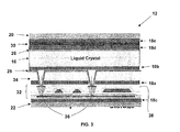
- Fig. 3 is a schematic sectional view of an LCD module, in accordance with one embodiment of the present invention.
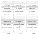
- Fig. 4 is a schematic flow diagram representing formation of an LTPS TFT array on a substrate of the LCD module, in accordance with one embodiment of the present invention.
- Figs. 5A to 5C are schematic flow diagrams representing formation of a digitizer sensor array in association with the formation of the LTPS-TFT array, in accordance with one embodiment of the present invention.
- Fig. 6 is a schematic flow diagram representing formation of an a-Si TFT array on a substrate of the LCD module, in accordance with one embodiment of the present invention.
- Figs. 7A to 7C are schematic flow diagrams representing formation of a digitizer sensor array in association with the formation of the a-Si TFT array, in accordance with one embodiment of the present invention.
- Figs. 8A to 8B are schematic flow diagrams representing formation of a digitizer sensor array about a front or back electrode near the substrate of the LCD module, in accordance with one embodiment of the present invention.
- Fig. 9 is a schematic flow diagram representing formation of a color filter on a substrate of the LCD module, in accordance with one embodiment of the present invention.
- Figs. 10A to 10C are schematic flow diagrams representing formation of a digitizer sensor array in association with the formation of the color display, in accordance with one embodiment of the present invention.
- Fig. 11 is a schematic sectional view of an OLED module, in accordance with one embodiment of the present invention.
- Fig. 12 is a schematic flow diagram representing formation of an AMOLED array on a substrate of the OLED module, in accordance with one embodiment of the present invention.
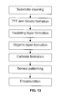
- Fig. 13 is a schematic flow diagram representing formation of a digitizer sensor array in association with the formation of the OLED array, in accordance with one embodiment of the present invention.
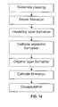
- Fig. 14 is a schematic flow diagram representing formation of a PMOLED array on a substrate of the OLED module, in accordance with one embodiment of the present invention.
- Fig. 15 is a schematic flow diagram representing formation of a digitizer sensor array in association with the formation of the PMOLED array, in accordance with one embodiment of the present invention.
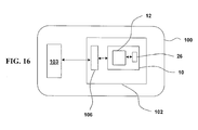
- Fig. 16 is a schematic representation of an electronic device incorporating the display device in accordance with one embodiment of the present invention.
- the present invention will be described in connection with flat panel LCD and OLED display devices, respectively having an LCD module and an OLED module as the display module, which respectively rely on LC elements and OLED elements as the display elements that can be controlled to render an image. Further, the present invention will be described in connection with an electromagnetic digitizer.
- the present invention is suitable for forming other types of digitizers, which may be incorporated in other types of display devices, flat panel or otherwise, having display modules comprising other types of display elements, such as cathode ray tubes (CRT), organic light emitting diode light emitting elements (OLED), field emission display (FED) elements, plasma light emitting elements, fluorescence light emitting elements, chemiluminescent light emitting elements, and other types of light emitting elements.
- CTR cathode ray tubes
- OLED organic light emitting diode light emitting elements
- FED field emission display
- plasma light emitting elements fluorescence light emitting elements
- chemiluminescent light emitting elements chemiluminescent light emitting elements
- other types of light emitting elements such as cathode ray tubes (CRT), organic light emitting diode light emitting elements (OLED), field emission display (FED) elements, plasma light emitting elements, fluorescence light emitting elements, chemiluminescent light emitting elements, and
- references to “on”, “above”, “overlying”, or other similar languages, are not limited to the interpretation of one layer being immediately adjacent another layer.
- references to steps undertaken “before”, “after”, “subsequent to”, “prior to”, “following” or the like are not limited to the interpretation of steps being undertaken immediately from one to another.
- references to structures adjacent, between or other positional references to other structures merely describe the relative positions of the structures, with or without intermediate structures.
- Fig. 2 illustrates a flat panel type display device 10 in accordance with one embodiment of the present invention, which includes an LCD module 12, and a backlight module 14 optically coupled to the LCD module 12.
- the LCD module 12 includes an LC layer 16, supported between two substrates 20 and 22, which can be controlled to regulate and/or filter light transmission to render a composite image based on pixilated image elements. Additional components have been omitted from Fig. 2, to simplify the structure for purpose of disclosing the inventive concept. For example, typically there are layers such as electrode layers, pixel control switches (e.g., thin film transistor (TFT) array), masking layers, LC alignment layers, color filter layers, and reflection layers within the LCD module 12 (some of these layers are shown in Fig.
- TFT thin film transistor
- the backlight module 14 may comprise a light source (not shown) that is positioned at an edge or at a planar side. In operation of the LCD module 10, light from the backlight module 14 is regulated, modulated and/or filtered by the LC layer 16, to render an image in accordance with an image data.
- a controller 26 controls the operation of the LCD module 10 (i.e., effecting control of the LC layer 16 via electrodes and drivers (not shown)). The controller 26 may be a part of the display device 10, and/or a part of a computing device to which the display device 10 is operatively attached.
- an electromagnetic digitizer 18 having the novel sensor segment structure of the present invention is supported between the LC layer 16 and the substrate 20, which is operatively coupled to the controller 26.
- the digitizer 18 may be positioned at other locations within the LCD module 12, for example between the LC layer 16 and the substrate 22, or at another intermediate layer location between the substrates 20 and 22 of the LCD module 12, as will be disclosed in further details below in reference to Fig. 3, for example.
- the digitizer 18 is integrated into the layers of the LCD module 12 of the display device 10, as opposed to the prior art display devices in which the digitizer panel is provided as a separate component outside the display module (e.g., outside the substrates of the LCD module as shown in Fig. 1). The overall size of the display device 10 is therefore reduced.
- a stylus 24 (e.g., in the shape of a pen) is provided.
- the stylus 24 is operatively coupled to the controller 26, either wirelessly or by a wire.
- the stylus 24 may include one or more button switches, which may be used to select certain input related modes or functions when pressed by a user (e.g., handwriting recognition mode, point and click mode, etc.)
- the stylus includes a magnetic element, which may be a permanent magnet or an electromagnet. As the stylus is moved across the substrate 20, its relative positional coordinates can be determined by the controller 26, based on a change in magnetic flux detected by the sensor segments within the electromagnetic digitizer.
- the basic operational principles of electromagnetic digitizers are well known in the art, and such would not be necessary to be disclosed here.
- the controller 26 controls and synchronizes the operations of the display module 12 including the digitizer, and the stylus. Images are controlled to be displayed by the display module 12, which may require user input by using the stylus to interact with the displayed image (e.g., making a selection by tapping on the display module, drawing or handwriting input by moving the stylus on the display module).
- the sensor array is formed as a layer or layers integrated within the various layers in the display module using semiconductor fabrication processes, as opposed to attached to the outside of the display module as practiced in the prior art.
- the sensor array may be formed on the side of the display element (e.g., LC layer or OLED layer) where the pixel control switches (e.g., thin film transistors (TFTs)) of the display module are present, or on the other side of the display element where the pixel control switches are not present.
- TFTs thin film transistors
- the sensor array may be formed (a) before planarization layer (or contact hole formation layer) of the pixel control switches (e.g., formed between the data line and the planarization layer), (b) after forming the planarization layer of the pixel control switches (e.g., formed after ITO patterning), (c) prior to forming the pixel control switches (e.g., formed on the substrate, before or after forming an electrode on the substrate), and/or (d) formed above or below a color filter layer above the display element, e.g., in the case of an LCD module, or above or below the encapsulating layer, e.g., in the case of an OLED display module.
- Fig. 3 is a schematic sectional view of the LCD module 12, indicating some of the possible locations of a digitizer 18 within the LCD module 12. (For simplicity, and for better reference, such possible alternative locations are shown together in Fig. 3, but they are not meant to be present concurrently at all the locations within the LC module 12.
- the digitizer may be alternatively located at 18a, 18b, 18c, 18d and 18e).
- the LCD module 12 includes the substrates 20 and 22, which may be glass.
- LC layer 16 Sandwiched between the substrates 20 and 22 is the LC layer 16, electrodes 28 and 29 about the LC layer 16 (which are used to provide a voltage bias across the LC layer 16 to regulate and/or filter light transmission to render a composite image based on pixilated image elements), a color filter 30 below the top substrate 20, and a TFT array 32 between the LC layer 16 and the bottom substrate 22.
- a planarization layer 34 (or contact hole formation layer) is provided between the TFT array 32 and the LC layer 16, through which vias of contact holes 36 are formed, through which electrical connections are made between the electrode 29 and the TFT array 32.
- the TFT array 32 includes an array of TFTs (each having a channel, and associated gate, source and drain) and complementary storage capacitors, wherein each TFT defined at the node of an array of orthogonal data lines and scan lines.
- the gate of the TFT is operatively connected to a data line and the source/drain is operatively connected to a scan line.
- the output surface of the LCD module 12 is the top substrate 20.
- the digitizer 18 may include a pair of sensor arrays (e.g., an X-array and a Y-array with sensor segments in the arrays that are orthogonal to each other), but the sensor arrays are collectively represented by the digitizer 18, and will so be collectively referenced hereinbelow.
- Fig. 3 five possible locations of the digitizer 18 are indicated within the LCD module 12. Three of the locations 18a, 18b and 18c are present on one side of the LC layer 16, the side at which the TFT array 32 is present. The other two locations 18d and 18e, are adjacent the color filter 30.
- the TFT array 32 may comprise TFTs that are of amorphous silicon (a-Si) type or low temperature polysilicon silicon (LTPS) type.
- a-Si amorphous silicon
- LTPS low temperature polysilicon silicon
- Fig. 4 is a diagram illustrating the flow process of forming a LTPS TFT
- Fig. 6 is a diagram illustrating the flow process of forming an a-Si TFT.
- the process for forming such includes generally the steps for forming a doped poly-Si channel region, a gate, and a source region and a drain regions (e.g., N+ and/or p+ regions).
- a data line is patterned to couple to the gate of the TFT via a contact hole in a dielectric layer 38.
- the resulting structure is covered with a planarization layer (34 in Fig. 3), prior to patterning the transparent electrode layer (29 in Fig. 3; an ITO layer).
- a planarization layer 34 in Fig. 3
- the sensor arrays within the digitizer 18a are patterned between formations of the data line and the planarization layer 34.
- the digitizer 18a is formed on a dielectric layer 38 above the data lines.
- Other steps not shown are undertaken to complete the LCD module 12.
- the sensor arrays within the digitizer 18b are patterned between formations of the transparent electrode 29 and the LC layer 16.
- a dielectric layer (not shown) may be provided above the transparent electrode 29 prior to forming the digitizer 18b, followed by formation of the LC layer 16 and the rest of the structures for the LC module 12.
- Fig. 5A to form the digitizer 18a, the sensor arrays within the digitizer 18a are patterned between formations of the data line and the planarization layer 34.
- the digitizer 18a is formed on a dielectric layer 38 above the data lines.
- Other steps not shown are undertaken to complete the LCD module 12.
- the digitizer 18c is formed on the bottom substrate 22, prior to forming the TFT array.
- the sensor arrays of the digitizer 18c may be patterned on the substrate, with or without a buffer layer, followed by the steps to form the LTPS TFT array, and the rest of the LC module 12.
- AMLCD active matrix LCD
- PMOS TFT array pixel control switches
- the LCD module 12 may include structures not shown, and requiring steps not shown, corresponding to transmissive, transflective, micro-reflective and reflective type LCD modules.
- the process for forming such includes generally the steps for forming a gate, patterning a-Si channel region, patterning data lines, and formation of contact holes in a dielectric layer 38 (which may involve a planarization layer), prior to patterning the transparent electrode layer (29 in Fig. 3; an ITO layer).
- a dielectric layer 38 which may involve a planarization layer
- ITO layer the transparent electrode layer
- the formation of the digitizer in an LCD display module with an a-Si TFT array is quite similar to the previous embodiment of the LTPS TFT array based LCD module.
- the sensor arrays of the digitizer is formed on the bottom substrate 22, prior to forming the a-Si TFT array.
- the sensor arrays of the digitizer 18c may be patterned on the substrate 22, with or without a buffer layer, followed by the steps to form the a-Si TFT array.
- the sensor arrays within the digitizer are patterned between formation of the data line and contact hole formation.
- the sensor arrays within the digitizer are patterned between formation of the transparent ITO electrode 29 and the LC layer 16.
- a dielectric layer (not shown) may be provided above the transparent electrode 29 prior to forming the digitizer 18b.
- the sensor arrays of the digitizer may be formed on the bottom substrate 22 with or without a buffer layer, similar to the processes in Fig. 5C and 7A above, prior to forming an electrode for the LC layer.
- the sensor arrays of the digitizer may be formed after forming the transparent electrode, such as ITO patterning. After formation of transparent electrode, a dielectric layer is deposited, followed by forming the sensor array of the digitizer, as shown in Fig. 8B. Following the steps shown in Figs.
- the top substrate 20 may involve a similar process, with respect to the sequence for forming the sensor arrays of the digitizer and the transparent electrode, as shown in Figs. 8A and 8B. Therefore, the flow processes shown in Fig. 8A and Fig. 8B are applicable for making both top and bottom substrates, depending on where the digitizer is desired.
- a digitizer is integrated with respect to the color filter 30.
- Fig. 9 is a diagram illustrating the flow process of forming the color filter 30 shown in Fig. 3 (without the digitizer 18).
- the process for forming such a color filter 30 generally includes the steps of substrate cleaning, spin coating of photo resist, pre-baking, exposing and developing of the photo resist, post baking of the developed photo resist, forming an overcoat of buffer or dielectric layer, and ITO sputtering to form the top common electrode 28 of the LC layer 16. This is done to include all the colors desired in the color filter layer 30 (e.g., red, green and blue).
- the sensor arrays within the digitizer 18d are patterned between formations of the overcoat and sputtering of the ITO electrode 28.
- the electrode 28 may be formed between the digitizer and the color filter 30 (not shown in Fig. 3).
- the sensor arrays within the digitizer are after formation of the transparent electrode 28 on the top substrate 20.
- the digitizer 18e is formed on the top substrate 20, with or without a buffer layer, prior to forming the color filter 32.
- top substrates 20 so formed with color filter 30, top electrode 20 and digitizer 18 can be assembled with the bottom substrate 22 that supports the TFT array 32 (which may be LTPS TFT or a-Si TFT), and providing the LC layer to complete the LC module structure shown in Fig. 3. Other steps not shown are undertaken to complete the LCD module 12.
- TFT array 32 which may be LTPS TFT or a-Si TFT
- Fig. 11 is a schematic sectional view of an OLED module 112 (having OLEDs as the display element), which, in this embodiment, is an active matrix OLED (AMOLED) module, and which indicates some of the possible locations of a digitizer 18 within the OLED module 112.
- AMOLED active matrix OLED
- the digitizer may be alternatively located at 18f, 18g, and 18h).
- the OLED module 112 includes a substrate 120 and 122, which may be glass.
- an OLED layer 116 (which generally comprises various sub-layers, including an electron transport layer 117, emissive layer 118 and hole transport layer 119), electrodes 28 (cathode) and 29 (anode) of the OLED layer 116 (which are used to provide a potential to drive the OLED layer 116 to emit light), an encapsulating layer 130 below the top substrate 20 (e.g., a glass cover of the overall structure), and a TFT array 32 between the LC layer 16 and the bottom substrate 122.
- a planarization layer 134 is provided between the TFT array 132 and the OLED layer 116, through which vias of contact holes 136 are formed, through which electrical connections are made between the electrode 129 and the TFT array 132.
- the digitizer 18 in this embodiment is similar to the previous embodiments.
- three possible locations of the digitizer 18 are indicated within the OLED module 112.
- Two of the locations 18f and 18g are present on one side of the OLED layer 116, the side at which the TFT array 132 is present.
- the other location 18f is adjacent the encapsulation layer 30.
- the TFT array 132 may comprise LTPS TFTs and/or a-Si TFTs, similar to the TFT array 32 disclosed in connection with the LCD module 12.
- the process for forming the digitizers 18f and 18g could be similar to the processes for digitizers 18a and 18c disclosed above in connection with Figs. 5A and 5C.
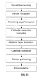
- the process for forming an AMOLED module includes generally the steps of cleaning the substrate 122, forming the anode 129 of the OLED, forming an insulating layer (hole transport layer), forming an organic layer of the OLED layer 116, forming the cathode 128, forming the encapsulating layer 130. There are additional steps not mentioned here, which are required to complete the OLED module 112, but which are not essential to an understanding of the present invention.
- the sensor arrays within the digitizer 18h are patterned between formations of the cathode 128 and the encapsulation layer 130, with a dielectric layer between the cathode 128 and the digitizer 18h. Other steps not shown are undertaken to complete the OLED module 112.
- the process for forming a passive matrix OLED (PMOLED) module includes generally the steps of cleaning the substrate 122, forming an anode of the OLED, forming an insulating layer (hole transport layer), forming a cathode separator, forming an organic layer of the OLED layer, forming a cathode, forming an encapsulating layer. There are additional steps not mentioned here, which are required to complete the OLED module 112, but which are not essential to an understanding of the present invention.
- the sensor arrays within the digitizer are patterned between formations of the cathode 128 and the encapsulation layer, similar to the process discussed in connection with Fig. 13 above. Other steps not shown are undertaken to complete the OLED module 112.
- Fig. 16 schematically shows an embodiment of an electronic device 100, which includes a display system 102 for displaying images, and an input/output (I/O) controller 103 for providing image data to the display system 102 and instructing the display system 102 to render an image in accordance with the image data.
- the display system 102 includes the display device 10 (e.g., an LCD device or an OLED display device) in accordance with the present invention and an interface controller 106 exchanging image data and user input data (from the digitizer 18) with the I/O controller 103.
- the display device incorporates a display module (e.g., an LCD module 12 or an OLED module 112) having an integrated electromagnetic digitizer 18 of the present invention and a controller 26 (e.g., drivers).
- the electronic device 100 may include a laptop computer, a mobile phone, a digital camera, a personal digital assistant (PDA), a desktop computer, a television, a car display or a portable DVD player.
- PDA personal digital assistant
Landscapes
- Physics & Mathematics (AREA)
- Engineering & Computer Science (AREA)
- Nonlinear Science (AREA)
- General Physics & Mathematics (AREA)
- Theoretical Computer Science (AREA)
- General Engineering & Computer Science (AREA)
- Optics & Photonics (AREA)
- Crystallography & Structural Chemistry (AREA)
- Chemical & Material Sciences (AREA)
- Mathematical Physics (AREA)
- Human Computer Interaction (AREA)
- Devices For Indicating Variable Information By Combining Individual Elements (AREA)
- Position Input By Displaying (AREA)
- Liquid Crystal (AREA)
Applications Claiming Priority (3)
| Application Number | Priority Date | Filing Date | Title |
|---|---|---|---|
| US70129705P | 2005-07-21 | 2005-07-21 | |
| US70116005P | 2005-07-21 | 2005-07-21 | |
| US11/311,986 US7924269B2 (en) | 2005-01-04 | 2005-12-20 | Display devices and methods forming the same |
Publications (1)
| Publication Number | Publication Date |
|---|---|
| EP1746485A2 true EP1746485A2 (de) | 2007-01-24 |
Family
ID=37036818
Family Applications (1)
| Application Number | Title | Priority Date | Filing Date |
|---|---|---|---|
| EP06117673A Withdrawn EP1746485A2 (de) | 2005-07-21 | 2006-07-21 | Verfahren zur Integration eines Digitalisiereingabegeräts in eine Anzeige |
Country Status (4)
| Country | Link |
|---|---|
| US (1) | US7852324B2 (de) |
| EP (1) | EP1746485A2 (de) |
| JP (1) | JP2007048279A (de) |
| KR (1) | KR20070012277A (de) |
Cited By (3)
| Publication number | Priority date | Publication date | Assignee | Title |
|---|---|---|---|---|
| EP2090966A1 (de) * | 2008-02-18 | 2009-08-19 | TPK Touch Solutions Inc. | Kapazitiver Berührungsbildschirm |
| US9395857B2 (en) | 2007-12-24 | 2016-07-19 | Tpk Holding Co., Ltd. | Capacitive touch panel |
| EP2422267B1 (de) * | 2009-04-20 | 2017-07-12 | Apple Inc. | Mit einer oled-struktur integrierte berührungsbetätigte sensorkonfiguration |
Families Citing this family (42)
| Publication number | Priority date | Publication date | Assignee | Title |
|---|---|---|---|---|
| US7663607B2 (en) | 2004-05-06 | 2010-02-16 | Apple Inc. | Multipoint touchscreen |
| TWI300672B (en) * | 2006-01-27 | 2008-09-01 | Au Optronics Corp | System integrated organic light-emitting display |
| CN104965621B (zh) | 2006-06-09 | 2018-06-12 | 苹果公司 | 触摸屏液晶显示器及其操作方法 |
| US8243027B2 (en) * | 2006-06-09 | 2012-08-14 | Apple Inc. | Touch screen liquid crystal display |
| KR101128543B1 (ko) | 2006-06-09 | 2012-03-23 | 애플 인크. | 터치 스크린 액정 디스플레이 |
| US20070283832A1 (en) * | 2006-06-09 | 2007-12-13 | Apple Computer, Inc. | Imprint circuit patterning |
| US7812827B2 (en) * | 2007-01-03 | 2010-10-12 | Apple Inc. | Simultaneous sensing arrangement |
| US8493330B2 (en) * | 2007-01-03 | 2013-07-23 | Apple Inc. | Individual channel phase delay scheme |
| US9710095B2 (en) | 2007-01-05 | 2017-07-18 | Apple Inc. | Touch screen stack-ups |
| US8493331B2 (en) | 2007-06-13 | 2013-07-23 | Apple Inc. | Touch detection using multiple simultaneous frequencies |
| TWI349221B (en) * | 2008-02-05 | 2011-09-21 | Au Optronics Corp | Sensing structure of a display |
| US8508495B2 (en) | 2008-07-03 | 2013-08-13 | Apple Inc. | Display with dual-function capacitive elements |
| US8592697B2 (en) | 2008-09-10 | 2013-11-26 | Apple Inc. | Single-chip multi-stimulus sensor controller |
| US9606663B2 (en) | 2008-09-10 | 2017-03-28 | Apple Inc. | Multiple stimulation phase determination |
| US9348451B2 (en) | 2008-09-10 | 2016-05-24 | Apple Inc. | Channel scan architecture for multiple stimulus multi-touch sensor panels |
| US9244568B2 (en) * | 2008-11-15 | 2016-01-26 | Atmel Corporation | Touch screen sensor |
| US8144295B2 (en) | 2008-11-18 | 2012-03-27 | Apple Inc. | Common bus design for a TFT-LCD display |
| US8749496B2 (en) * | 2008-12-05 | 2014-06-10 | Apple Inc. | Integrated touch panel for a TFT display |
| US8217913B2 (en) | 2009-02-02 | 2012-07-10 | Apple Inc. | Integrated touch screen |
| US7995041B2 (en) * | 2009-02-02 | 2011-08-09 | Apple Inc. | Integrated touch screen |
| US20100265187A1 (en) * | 2009-04-20 | 2010-10-21 | Shih Chang Chang | Signal routing in an oled structure that includes a touch actuated sensor configuration |
| US8576161B2 (en) * | 2009-06-18 | 2013-11-05 | Apple Inc. | Driving an OLED display structure integrated with a touch sensor configuration |
| CN101930134B (zh) * | 2009-06-19 | 2013-08-07 | 台均科技(深圳)有限公司 | 电磁感应式液晶面板及其制造方法和液晶显示器 |
| CN101937280A (zh) * | 2009-07-01 | 2011-01-05 | 鸿富锦精密工业(深圳)有限公司 | 触控系统及其文件浏览方法 |
| KR101663034B1 (ko) * | 2009-08-26 | 2016-10-07 | 삼성디스플레이 주식회사 | 접촉 감지 기능이 있는 전기 영동 표시 장치 |
| TWI416385B (zh) * | 2009-12-18 | 2013-11-21 | Au Optronics Corp | 三維互動立體顯示器之指示物位置判斷方法 |
| US8804056B2 (en) * | 2010-12-22 | 2014-08-12 | Apple Inc. | Integrated touch screens |
| US9064451B2 (en) * | 2012-02-01 | 2015-06-23 | Apple Inc. | Organic light emitting diode display having photodiodes |
| US9395583B2 (en) | 2012-06-06 | 2016-07-19 | Apple Inc. | Column spacer design for a display incorporating a third metal layer |
| CN102707480B (zh) * | 2012-06-28 | 2015-01-07 | 旭曜科技股份有限公司 | 内嵌式多点触控液晶显示面板系统 |
| KR101391243B1 (ko) | 2012-07-17 | 2014-05-02 | 삼성디스플레이 주식회사 | 터치 인식 기능을 가지는 표시장치 |
| US9336723B2 (en) | 2013-02-13 | 2016-05-10 | Apple Inc. | In-cell touch for LED |
| US9224790B2 (en) * | 2013-11-13 | 2015-12-29 | Industrial Technology Research Institute | Illumination device |
| US9395072B2 (en) | 2013-11-13 | 2016-07-19 | Industrial Technology Research Institute | Illumination device |
| KR101984443B1 (ko) | 2013-12-13 | 2019-05-30 | 애플 인크. | 자기-정전용량성 터치 센서를 위한 통합된 터치 및 디스플레이 아키텍처 |
| WO2015160377A1 (en) | 2014-04-16 | 2015-10-22 | Wrostix Technologies Llc | Structure for pixelated self-capacitance |
| US10133382B2 (en) | 2014-05-16 | 2018-11-20 | Apple Inc. | Structure for integrated touch screen |
| US9367188B2 (en) | 2014-05-23 | 2016-06-14 | Apple Inc. | RC matching in a touch screen |
| WO2015183334A1 (en) | 2014-05-28 | 2015-12-03 | Pylemta Management Llc | Narrow border touch screen |
| KR102244650B1 (ko) | 2014-10-24 | 2021-04-28 | 삼성디스플레이 주식회사 | 표시 장치 |
| CN109075446B (zh) * | 2016-01-29 | 2020-09-08 | 夏普株式会社 | 天线设备 |
| KR102413361B1 (ko) * | 2018-02-23 | 2022-06-27 | 동우 화인켐 주식회사 | Oled 일체형 디지타이저 및 그 제조 방법 |
Citations (1)
| Publication number | Priority date | Publication date | Assignee | Title |
|---|---|---|---|---|
| US20060146033A1 (en) | 2005-01-04 | 2006-07-06 | Toppoly Optoelectronics Corp. | Display devices and methods forming the same |
Family Cites Families (17)
| Publication number | Priority date | Publication date | Assignee | Title |
|---|---|---|---|---|
| JPH04222018A (ja) * | 1990-12-25 | 1992-08-12 | Fujitsu Ltd | 入出力装置 |
| US5821916A (en) * | 1992-08-13 | 1998-10-13 | Calcomp, Inc. | Digitizer cursor velocity offset error correction system |
| US5644653A (en) * | 1993-05-07 | 1997-07-01 | Canon Kabushiki Kaisha | Information processing apparatus and control method thereof having user character recognition |
| KR100300397B1 (ko) * | 1994-04-21 | 2001-10-22 | 김순택 | 터치판넬및디지타이저기능을겸비한시스템및구동방법 |
| JPH0980467A (ja) | 1995-09-14 | 1997-03-28 | Toshiba Corp | ペン入力位置の検出機能を有するアクティブマトリックス型表示装置 |
| JPH09258893A (ja) | 1996-03-25 | 1997-10-03 | Toshiba Corp | 座標入力装置、およびこれを備えた入力表示装置 |
| KR100293435B1 (ko) * | 1997-10-31 | 2001-08-07 | 구본준, 론 위라하디락사 | 위치검출액정디스플레이장치(pslcd)및이의제조방법 |
| JP3466081B2 (ja) | 1998-03-20 | 2003-11-10 | 株式会社東芝 | 液晶表示装置および位置検出装置 |
| KR100534376B1 (ko) * | 1999-06-21 | 2005-12-08 | 엘지.필립스 엘시디 주식회사 | 디지타이저를 가진 액정표시소자 |
| KR20010030164A (ko) | 1999-08-31 | 2001-04-16 | 고지마 아끼로, 오가와 다이스께 | 터치 패널 및 그것을 이용한 표시 장치 |
| JP2001085160A (ja) * | 1999-09-20 | 2001-03-30 | Nec Corp | 発光出力補正機能付き発光素子 |
| JP2001183630A (ja) | 1999-12-24 | 2001-07-06 | Casio Comput Co Ltd | 座標入力機能付き表示装置 |
| JP4507480B2 (ja) | 2001-12-27 | 2010-07-21 | ソニー株式会社 | 表示装置 |
| TW571161B (en) * | 2002-07-30 | 2004-01-11 | Au Optronics Corp | A flat panel display in which a digitizer is integrated |
| US7755616B2 (en) * | 2003-03-28 | 2010-07-13 | Lg Display Co., Ltd. | Liquid crystal display device having electromagnetic type touch panel |
| US7298367B2 (en) * | 2003-11-25 | 2007-11-20 | 3M Innovative Properties Company | Light emitting stylus and user input device using same |
| US7265303B2 (en) * | 2003-12-17 | 2007-09-04 | Microsoft Corporation | Electromagnetic digitizer sensor array |
-
2006
- 2006-07-21 EP EP06117673A patent/EP1746485A2/de not_active Withdrawn
- 2006-07-21 KR KR1020060068756A patent/KR20070012277A/ko not_active Withdrawn
- 2006-07-21 JP JP2006199501A patent/JP2007048279A/ja active Pending
- 2006-07-21 US US11/490,835 patent/US7852324B2/en active Active
Patent Citations (1)
| Publication number | Priority date | Publication date | Assignee | Title |
|---|---|---|---|---|
| US20060146033A1 (en) | 2005-01-04 | 2006-07-06 | Toppoly Optoelectronics Corp. | Display devices and methods forming the same |
Cited By (5)
| Publication number | Priority date | Publication date | Assignee | Title |
|---|---|---|---|---|
| US9395857B2 (en) | 2007-12-24 | 2016-07-19 | Tpk Holding Co., Ltd. | Capacitive touch panel |
| EP2090966A1 (de) * | 2008-02-18 | 2009-08-19 | TPK Touch Solutions Inc. | Kapazitiver Berührungsbildschirm |
| EP2090967A1 (de) * | 2008-02-18 | 2009-08-19 | TPK Touch Solutions Inc. | Kapazitiver Berührungsbildschirm |
| US8665226B2 (en) | 2008-02-18 | 2014-03-04 | Tpk Touch Solutions Inc. | Capacitive touch panel |
| EP2422267B1 (de) * | 2009-04-20 | 2017-07-12 | Apple Inc. | Mit einer oled-struktur integrierte berührungsbetätigte sensorkonfiguration |
Also Published As
| Publication number | Publication date |
|---|---|
| JP2007048279A (ja) | 2007-02-22 |
| US7852324B2 (en) | 2010-12-14 |
| US20070018969A1 (en) | 2007-01-25 |
| KR20070012277A (ko) | 2007-01-25 |
Similar Documents
| Publication | Publication Date | Title |
|---|---|---|
| US7852324B2 (en) | Process of integrating a digitizer input device in a display | |
| US11422652B2 (en) | Display device with integrated touch screen | |
| US7875814B2 (en) | Electromagnetic digitizer sensor array structure | |
| US10613664B2 (en) | Display device with built-in touch screen and method of fabricating the same | |
| CN108268168B (zh) | 具有集成触摸屏的显示装置及其制造方法 | |
| US10739918B2 (en) | Display device integrated with touch screen panel and method of fabricating the same | |
| US9536913B2 (en) | Display device integrated with touch screen panel and method for fabricating the same | |
| US10860123B2 (en) | Display device with integrated touch screen and method of manufacturing the same | |
| US20080084366A1 (en) | Display device | |
| CN113410257B (zh) | 阵列基板、显示面板及显示装置 | |
| US20180095581A1 (en) | Organic Light Emitting Display Device | |
| JP4873410B2 (ja) | 電磁デジタイザセンサアレイ構造 | |
| CN105278728B (zh) | 集成有触摸屏面板的显示设备及其制造方法 | |
| US8411059B2 (en) | Integrated electromagnetic type input flat panel display apparatus | |
| WO2016033928A1 (zh) | 显示面板及其驱动方法、显示装置 | |
| US20210193819A1 (en) | Thin film transistor array substrate and its manufacturing method and oled touch display device | |
| CN111694464B (zh) | 阵列基板及其制备方法、显示装置 | |
| CN117826486A (zh) | 显示装置 | |
| US20210216164A1 (en) | Touch-sensing display substrate, touch-sensing display apparatus, method of operating touch-sensing display apparatus, and method of fabricating touch-sensing display substrate | |
| US11137849B2 (en) | Touch display device and manufacturing method thereof | |
| US10620468B2 (en) | Method of manufacturing display panel substrate |
Legal Events
| Date | Code | Title | Description |
|---|---|---|---|
| PUAI | Public reference made under article 153(3) epc to a published international application that has entered the european phase |
Free format text: ORIGINAL CODE: 0009012 |
|
| AK | Designated contracting states |
Kind code of ref document: A2 Designated state(s): AT BE BG CH CY CZ DE DK EE ES FI FR GB GR HU IE IS IT LI LT LU LV MC NL PL PT RO SE SI SK TR |
|
| AX | Request for extension of the european patent |
Extension state: AL BA HR MK YU |
|
| STAA | Information on the status of an ep patent application or granted ep patent |
Free format text: STATUS: THE APPLICATION IS DEEMED TO BE WITHDRAWN |
|
| 18D | Application deemed to be withdrawn |
Effective date: 20100201 |