EP1746565A2 - Dispositif d'affichage à électroluminescence organique et son procédé de commande - Google Patents
Dispositif d'affichage à électroluminescence organique et son procédé de commande Download PDFInfo
- Publication number
- EP1746565A2 EP1746565A2 EP06007906A EP06007906A EP1746565A2 EP 1746565 A2 EP1746565 A2 EP 1746565A2 EP 06007906 A EP06007906 A EP 06007906A EP 06007906 A EP06007906 A EP 06007906A EP 1746565 A2 EP1746565 A2 EP 1746565A2
- Authority
- EP
- European Patent Office
- Prior art keywords
- electro luminescence
- current
- data
- supplied
- charge
- Prior art date
- Legal status (The legal status is an assumption and is not a legal conclusion. Google has not performed a legal analysis and makes no representation as to the accuracy of the status listed.)
- Granted
Links
Images




Classifications
-
- G—PHYSICS
- G09—EDUCATION; CRYPTOGRAPHY; DISPLAY; ADVERTISING; SEALS
- G09G—ARRANGEMENTS OR CIRCUITS FOR CONTROL OF INDICATING DEVICES USING STATIC MEANS TO PRESENT VARIABLE INFORMATION
- G09G3/00—Control arrangements or circuits, of interest only in connection with visual indicators other than cathode-ray tubes
- G09G3/20—Control arrangements or circuits, of interest only in connection with visual indicators other than cathode-ray tubes for presentation of an assembly of a number of characters, e.g. a page, by composing the assembly by combination of individual elements arranged in a matrix no fixed position being assigned to or needed to be assigned to the individual characters or partial characters
- G09G3/22—Control arrangements or circuits, of interest only in connection with visual indicators other than cathode-ray tubes for presentation of an assembly of a number of characters, e.g. a page, by composing the assembly by combination of individual elements arranged in a matrix no fixed position being assigned to or needed to be assigned to the individual characters or partial characters using controlled light sources
- G09G3/30—Control arrangements or circuits, of interest only in connection with visual indicators other than cathode-ray tubes for presentation of an assembly of a number of characters, e.g. a page, by composing the assembly by combination of individual elements arranged in a matrix no fixed position being assigned to or needed to be assigned to the individual characters or partial characters using controlled light sources using electroluminescent panels
- G09G3/32—Control arrangements or circuits, of interest only in connection with visual indicators other than cathode-ray tubes for presentation of an assembly of a number of characters, e.g. a page, by composing the assembly by combination of individual elements arranged in a matrix no fixed position being assigned to or needed to be assigned to the individual characters or partial characters using controlled light sources using electroluminescent panels semiconductive, e.g. using light-emitting diodes [LED]
- G09G3/3208—Control arrangements or circuits, of interest only in connection with visual indicators other than cathode-ray tubes for presentation of an assembly of a number of characters, e.g. a page, by composing the assembly by combination of individual elements arranged in a matrix no fixed position being assigned to or needed to be assigned to the individual characters or partial characters using controlled light sources using electroluminescent panels semiconductive, e.g. using light-emitting diodes [LED] organic, e.g. using organic light-emitting diodes [OLED]
- G09G3/3216—Control arrangements or circuits, of interest only in connection with visual indicators other than cathode-ray tubes for presentation of an assembly of a number of characters, e.g. a page, by composing the assembly by combination of individual elements arranged in a matrix no fixed position being assigned to or needed to be assigned to the individual characters or partial characters using controlled light sources using electroluminescent panels semiconductive, e.g. using light-emitting diodes [LED] organic, e.g. using organic light-emitting diodes [OLED] using a passive matrix
-
- G—PHYSICS
- G09—EDUCATION; CRYPTOGRAPHY; DISPLAY; ADVERTISING; SEALS
- G09G—ARRANGEMENTS OR CIRCUITS FOR CONTROL OF INDICATING DEVICES USING STATIC MEANS TO PRESENT VARIABLE INFORMATION
- G09G3/00—Control arrangements or circuits, of interest only in connection with visual indicators other than cathode-ray tubes
- G09G3/20—Control arrangements or circuits, of interest only in connection with visual indicators other than cathode-ray tubes for presentation of an assembly of a number of characters, e.g. a page, by composing the assembly by combination of individual elements arranged in a matrix no fixed position being assigned to or needed to be assigned to the individual characters or partial characters
- G09G3/22—Control arrangements or circuits, of interest only in connection with visual indicators other than cathode-ray tubes for presentation of an assembly of a number of characters, e.g. a page, by composing the assembly by combination of individual elements arranged in a matrix no fixed position being assigned to or needed to be assigned to the individual characters or partial characters using controlled light sources
- G09G3/30—Control arrangements or circuits, of interest only in connection with visual indicators other than cathode-ray tubes for presentation of an assembly of a number of characters, e.g. a page, by composing the assembly by combination of individual elements arranged in a matrix no fixed position being assigned to or needed to be assigned to the individual characters or partial characters using controlled light sources using electroluminescent panels
-
- G—PHYSICS
- G09—EDUCATION; CRYPTOGRAPHY; DISPLAY; ADVERTISING; SEALS
- G09G—ARRANGEMENTS OR CIRCUITS FOR CONTROL OF INDICATING DEVICES USING STATIC MEANS TO PRESENT VARIABLE INFORMATION
- G09G2310/00—Command of the display device
- G09G2310/02—Addressing, scanning or driving the display screen or processing steps related thereto
- G09G2310/0243—Details of the generation of driving signals
- G09G2310/0248—Precharge or discharge of column electrodes before or after applying exact column voltages
-
- G—PHYSICS
- G09—EDUCATION; CRYPTOGRAPHY; DISPLAY; ADVERTISING; SEALS
- G09G—ARRANGEMENTS OR CIRCUITS FOR CONTROL OF INDICATING DEVICES USING STATIC MEANS TO PRESENT VARIABLE INFORMATION
- G09G2320/00—Control of display operating conditions
- G09G2320/02—Improving the quality of display appearance
- G09G2320/0209—Crosstalk reduction, i.e. to reduce direct or indirect influences of signals directed to a certain pixel of the displayed image on other pixels of said image, inclusive of influences affecting pixels in different frames or fields or sub-images which constitute a same image, e.g. left and right images of a stereoscopic display
-
- G—PHYSICS
- G09—EDUCATION; CRYPTOGRAPHY; DISPLAY; ADVERTISING; SEALS
- G09G—ARRANGEMENTS OR CIRCUITS FOR CONTROL OF INDICATING DEVICES USING STATIC MEANS TO PRESENT VARIABLE INFORMATION
- G09G2320/00—Control of display operating conditions
- G09G2320/02—Improving the quality of display appearance
- G09G2320/0285—Improving the quality of display appearance using tables for spatial correction of display data
-
- G—PHYSICS
- G09—EDUCATION; CRYPTOGRAPHY; DISPLAY; ADVERTISING; SEALS
- G09G—ARRANGEMENTS OR CIRCUITS FOR CONTROL OF INDICATING DEVICES USING STATIC MEANS TO PRESENT VARIABLE INFORMATION
- G09G3/00—Control arrangements or circuits, of interest only in connection with visual indicators other than cathode-ray tubes
- G09G3/20—Control arrangements or circuits, of interest only in connection with visual indicators other than cathode-ray tubes for presentation of an assembly of a number of characters, e.g. a page, by composing the assembly by combination of individual elements arranged in a matrix no fixed position being assigned to or needed to be assigned to the individual characters or partial characters
- G09G3/22—Control arrangements or circuits, of interest only in connection with visual indicators other than cathode-ray tubes for presentation of an assembly of a number of characters, e.g. a page, by composing the assembly by combination of individual elements arranged in a matrix no fixed position being assigned to or needed to be assigned to the individual characters or partial characters using controlled light sources
- G09G3/30—Control arrangements or circuits, of interest only in connection with visual indicators other than cathode-ray tubes for presentation of an assembly of a number of characters, e.g. a page, by composing the assembly by combination of individual elements arranged in a matrix no fixed position being assigned to or needed to be assigned to the individual characters or partial characters using controlled light sources using electroluminescent panels
- G09G3/32—Control arrangements or circuits, of interest only in connection with visual indicators other than cathode-ray tubes for presentation of an assembly of a number of characters, e.g. a page, by composing the assembly by combination of individual elements arranged in a matrix no fixed position being assigned to or needed to be assigned to the individual characters or partial characters using controlled light sources using electroluminescent panels semiconductive, e.g. using light-emitting diodes [LED]
- G09G3/3208—Control arrangements or circuits, of interest only in connection with visual indicators other than cathode-ray tubes for presentation of an assembly of a number of characters, e.g. a page, by composing the assembly by combination of individual elements arranged in a matrix no fixed position being assigned to or needed to be assigned to the individual characters or partial characters using controlled light sources using electroluminescent panels semiconductive, e.g. using light-emitting diodes [LED] organic, e.g. using organic light-emitting diodes [OLED]
- G09G3/3275—Details of drivers for data electrodes
- G09G3/3283—Details of drivers for data electrodes in which the data driver supplies a variable data current for setting the current through, or the voltage across, the light-emitting elements
Definitions
- the present invention relates to an organic electro luminescence display device, and more particularly to an organic electro luminescence display device using pre-charge, and a driving method thereof.
- the flat panel display device includes liquid crystal display (hereinafter, referred to as "LCD”), field emission display (hereinafter, referred to as “FED”), plasma display panel (hereinafter, referred to as “PDP”), and electroluminescence display (hereinafter, referred to as "EL").
- LCD liquid crystal display
- FED field emission display
- PDP plasma display panel
- EL electroluminescence display
- the PDP has a relatively simple structure and fabricating process, thus the PDP is advantageous in being made into a large screen, but there is a disadvantage in that its light emission efficiency and brightness is low and its power consumption is high.
- the LCD has its demand increased as it is mainly used as a display device of a notebook computer.
- the LCD is fabricated by a semiconductor process, thus it is difficult to be made into the large screen.
- the LCD is not a self-luminous device, there is a disadvantage in that a separate light source is required and power consumption is big due to the light source.
- the LCD has a disadvantage in that a lot of light loss is caused by optical devices such as a polarizing filter, a prism sheet, a diffusion plate, etc and its viewing angle is narrow.
- the EL display device is roughly divided into an inorganic EL display device and an organic EL display device, and has an advantage in that its response speed is fast and its light emission efficiency, brightness and viewing angle are high.
- the organic EL display device can display a picture in a high brightness of tens of thousands [cd/m 2 ] with a voltage of about 10[V] or so, and is applied to most of the EL display devices which are put to practical use.
- a unit device of the organic EL display device forms an anode 2 of transparent conductive material on a glass substrate 1, and a hole injection layer 3, a light emitting layer of organic material and a cathode 5 of metal of which a work function is low, on top thereof. If an electric field is applied between the anode 2 and the cathode 5, holes within the hole injection layer 3 and electrons within the metal respectively move toward the light emitting layer 4 to be combined with each other in the light emitting layer 4. Then, a fluorescent material within the light emitting layer 4 is excited to have a transition made, thereby generating a visible ray. At this moment, the brightness is proportional to a current between the anode 2 and the cathode 5.
- the organic EL display device is divided into a passive type and an active type.
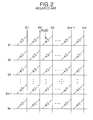
- FIG. 2 is a circuit diagram equivalently representing a part of an organic EL display device of a passive type
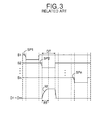
- FIG. 3 is a waveform diagram representing waveforms of a scan signal and a data signal of the passive type organic EL display device.
- the passive type organic EL display device includes a plurality of data lines D1 to Dm and a plurality of scan lines S1 to Sn which cross each other; and organic EL cells OLED respectively formed at the crossing parts between the data lines D1 to Dm and the scan lines S1 to Sn.
- the data lines D1 to Dm are connected to the anode of the organic EL device OLED to supply a data current Id to the anode of the organic EL device OLED.
- the scan lines S1 to Sn is connected to the cathode of the organic EL cell OLED to supply scan pulses SP1 to SPn synchronized with the data current Id to the cathode of the organic EL cell OLED.
- the organic EL cell OLED emits light in proportion to the current flowing between the anode and the cathode during a display period DT when the scan pulses SP1 to SPn are applied.
- the organic EL cell OLED of the organic EL display device has a problem that its response speed is low and its brightness is low because a current is charged therein during a response time RT delayed by a capacitance existing in the organic EL cell OLED and a resistance component of the data lines D1 to Dm.
- a pre-charge period is provided as a non-display period between display periods DT.
- a pre-charge voltage waveform in contradiction to the same pre-charge period is made differently in accordance with locations of the data lines D1 to Dm and the scan lines S1 to Sn, thereby generating a problem such as a horizontal cross talk.
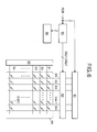
- FIG. 4 represents a still picture has a black picture realized in the middle of the picture and a white picture realized in an area except the black picture.
- first white area A a white picture area horizontally adjacent to and a white picture area (hereinafter, referred to as "second white area B") vertically adjacent to the area where the black picture is realized.
- second white area B a white picture area vertically adjacent to the area where the black picture is realized.
- the organic EL cells OLED corresponding to the black picture area in an (N+1) th scan line do not emit light, thus the loading quantity corresponding to non-light-emitting organic EL cells OLED is excluded from the total loading quantity in the (N+1) th scan line. Accordingly, a higher drive voltage is charged in the second white area B than in the first white area A, wherein the second white area B corresponds to the N th scan line of which the loading quantity is relatively larger than the (N+1) th scan line.
- the amount of the current charged in the data line corresponding to the (N+1) th scan line in contradiction to the same pre-charge period is relatively lower than the amount of the current charged in the data line corresponding to the N th scan line, thus there is generated a cross talk problem by the brightness difference (or drive voltage deviation) between the first white area A and the second white area B although the same data current and pre-charge current is supplied for expressing the same gray level.
- an object of the present invention to provide an organic EL display device using pre-charge which can improve display quality by preventing a cross talk generated by a brightness difference within the same picture realization area, and a driving method thereof.
- an organic electro luminescence display device includes a display panel where a plurality of data lines cross a plurality of scan lines and electro luminescence cells are arranged in the crossing parts thereof; a pre-charge driver for supplying a pre-charge current to the data line in accordance with gray levels of data; and a data driver for charging a data current to the data line for a designated period which is set before a scan pulse is supplied to the electro luminescence cell and after the pre-charge current is supplied.
- the data driver supplies the data current for electro luminescence to the electro luminescence cell at the same time as a scan pulse is supplied to the electro luminescence cell.
- the organic electro luminescence display device further includes a scan driver for supplying the scan pulse synchronized with the data current supplied to the electro luminescence cell to the scan lines.
- the designated period before the scan pulse is supplied to the electro luminescence cells and after the pre-charge current is supplied is obtained from a light emitting period of the electro luminescence cell.
- the designated period before the scan pulse is supplied to the electro luminescence cells and after the pre-charge current is supplied is obtained by maintaining the light emitting period of the electro luminescence cells and by lengthening a period from a starting point of the scan pulse to a starting point of the next scan pulse.
- the organic electro luminescence display device further includes a lookup table having pre-charge current data registered, wherein the pre-charge current data indicates the current amount of the pre-charge current corresponding to a gray level of the data; and a controller for controlling the pre-charge driver in accordance with the supply of the data current and the pre-charge current.
- the pre-charge driver includes a plurality of current sources of which the current values are different from each other; a selector for selecting any one of the current sources as the pre-charge current; and first and second switch devices for selectively supplying the pre-charge current and the data current to the data line.
- an early increase and decrease rate and a latter increase and decrease rate of a current charged in the data line for the designated period before the scan pulse is supplied to the electro luminescence cells and after the pre-charge current is supplied are different from each other.
- an early increase and decrease rate of a current charged in the data line for the designated period before the scan pulse is supplied to the electro luminescence cells and after the pre-charge current is supplied is higher than the latter increase and decrease rate.
- a driving method of an organic electro luminescence display device where a plurality of data lines cross a plurality of scan lines and electro luminescence cells are arranged in the crossing parts thereof includes supplying a pre-charge current to the data line in accordance with gray levels of data; charging a data current to the data line for a designated period which is set before a scan pulse is supplied to the electro luminescence cell and after the pre-charge current is supplied; and making the electro luminescence cells emit light by use of the charged current and the data current synchronized with the scan pulse to be supplied to the electro luminescence cell.
- the designated period before the scan pulse is supplied to the electro luminescence cells and after the pre-charge current is supplied is obtained from a light emitting period of the electro luminescence cell.
- the designated period before the scan pulse is supplied to the electro luminescence cells and after the pre-charge current is supplied is obtained by maintaining the light emitting period of the electro luminescence cells and by lengthening a period from a starting point of the scan pulse to a starting point of the next scan pulse.
- an early increase and decrease rate and a latter increase and decrease rate of a current charged in the data line for the designated period before the scan pulse is supplied to the electro luminescence cells and after the pre-charge current is supplied are different from each other.
- an early increase and decrease rate of a current charged in the data line for the designated period before the scan pulse is supplied to the electro luminescence cells and after the pre-charge current is supplied is higher than the latter increase and decrease rate.
- an organic EL display device includes a display panel 64 where m x n number of organic EL cells OLED are arranged in a matrix type; a data driver 61 for generating a data current; a pre-charge driver 62 for generating a pre-charge current; a scan driver 63 for generating a scan pulse synchronized with the data current; and a pre-charge/data controller 65 for controlling the pre-charge driver 62.
- m number of data lines D1 to Dm cross n number of scan lines S1 to Sn, and the organic EL cells OLED are arranged between the crossing parts thereof.
- the data driver 61 includes a shift register circuit for sequentially sampling data, and a current source such as a current mirror circuit or a current sink circuit.
- the data driver 61 samples digital video data, and supplies the data current corresponding to the gray level value of the digital video data RGB to the data lines D1 to Dm through the pre-charge driver 62.
- the scan driver 63 includes a shift register circuit for sequentially shifting scan pulses, and sequentially supplies the scan pulses synchronized with the data currents to the scan lines S1 to Sn.
- the pre-charge driver 62 supplies the pre-charge current to the data lines D1 to Dm prior to the data current under control of the pre-charge/data controller 65.
- the pre-charge/data controller 65 judges the gray level value of the digital video data RGB, and reads pre-charge current data corresponding to the gray level value from a lookup table 66. And, the pre-charge/data controller 65 receives a clock signal and a vertical/horizontal synchronization signal (not shown) to selectively generate control signals SEL1, SEL2 corresponding to the pre-charge current data, and controls the pre-charge driver 62 by use of the control signals SEL1, SEL2.
- the first control signal SEL1 is a control signal generated for a pre-charge period prior to a scan period (or light emitting period) and a delay period to select the amount of the pre-charge current for supplying the pre-charge current to the data lines D1 to Dm for the pre-charge period.
- the second control signal SEL2 is a control signal for supplying the data current to the data lines D1 to Dm as well as intercepting the supply of the pre-charge current after the pre-charge period.
- the lookup table 66 has the pre-charge current data registered, wherein the pre-charge current data correspond to each gray level of the digital video data RGB.
- FIG. 7 represents a pre-charge driver 62 in detail.
- the pre-charge driver 62 shown in FIG. 7 includes a selector 71 for selecting the current amount of a pre-charge current Ipre; a first switch device 72A for supplying the pre-charge current Ipre to the data line D; and a second switch device 72B for supplying a data current Id1 to the data line D.
- the second switch device 72B might be included in the data driver 61.
- the current selector 71 selects the pre-charge current Ipre in any one of k (but, 'k' is a positive integer of 2 or more) number of current sources 11, 12, ..., Ik, of which the current amount is different from each other, to supply to the first switch device 72A in response to a first selection signal SEL1 from the pre-charge/data controller 65.
- the first switch device 72A supplies the pre-charge current Ipre selected by the current selector 71 to the data line for the pre-charge period prior to the light emitting period and the delay period in response to the first selection signal SEL1 from the pre-charge/data controller 65.
- the second switch device 72B supplies the data current Id1 from the data driver 61 to the data line D1 for the delay period and the light emitting period in response to the second selection signal SEL2 from the pre-charge/data controller 65.
- FIG. 8 is a circuit diagram equivalently representing the data line D and the organic EL cell OLED of the display panel and the drive circuit shown in FIG. 7.
- the reference numeral 'R' is a parasitic resistance between the organic EL devices OLED in the data line
- 'CAP' is a parasitic capacitance of the organic EL cell OLED.
- '61A' is a static current source included in the data driver 61 and generates the data current.
- '63A' is a switch device included in the scan driver 63, and applies a ground voltage GND to a cathode of the organic EL cell OLED for the light emitting period (or display period) and supplies a positive scan bias voltage to the cathode of the organic EL cell OLED for a non-display period inclusive of the pre-charge period and the delay period except the light emitting period.
- 'VDD' is a high potential drive voltage applied to the static current source 61A
- 'VSS' is a scan bias voltage applied to the cathode of the organic EL cell OLED for the non-display period, i.e., for the non-scan period.
- a delay period DT which is a period before a scan pulse SP from the scan driver 63 is supplied to the organic EL cell OLED after the pre-charge current is supplied from the pre-charge driver 62.
- the scan pulse SP is not applied to the organic EL cell OLED, but the data current is made to be able to be charged in the data line D, thereby enabling to prevent the brightness difference between areas which express the same gray level. As a result, it is possible to prevent a horizontal cross talk.
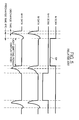
- the amount of the current charged in the data line corresponding to the (N+1) th scan line in contradiction to the same pre-charge period PT is relatively lower than the amount of the current charged in the data line corresponding to the N th scan line in accordance with the difference of the loading quantity between the (N+1) th scan line and the N th scan line.
- the data current is supplied to the data line, but no scan pulse SP is supplied to the scan line. Accordingly, the organic EL cell OLED does not emit light, and the data current can only be charged in the data line.
- the delay period Dt the amount of the current charged in the data lines corresponding to the (N+1) th scan line of which the loading quantity is relatively low is increased, and the amount of the current charged in the data lines corresponding to the N th scan line of which the loading quantity is relatively high is reduced.
- the present invention has the pre-charge period PT and the delay period DT before the scan pulse SP is supplied, thereby enabling to compensate the brightness difference in accordance with the difference of the loading quantity in the horizontal line.
- a problem such as cross talk, etc does not appear, thereby making it possible to improve the display quality.
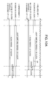
- FIG. 10A a first method of providing the delay period DT of the present invention is illustrated in FIG. 10A.
- an applying time of the scan pulse SP is reduced more than the related art and the applying time the reduced scan pulse SP is used as the delay period DT.
- times (hereinafter, referred to as 'scan period') from a starting point of the N th scan pulse SP to a starting point of the (N+1) th scan pulse SP are maintained identically, and a time (hereinafter, referred to as 'light emitting period' or 'display period') when the scan pulse SP is in fact applied is set to be shorter than the related art, thereby providing the delay period DT.
- the light emitting period is shortened as much as the number of the increased clocks for the delay period DT, thus there is no change in the frame frequency.
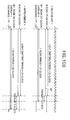
- the light emitting period is maintained but the scan period is lengthened, thereby providing the delay period DT.
- the N th and (N+1) th light emitting periods are maintained and the scan period from the starting point of the N th scan pulse SP to the starting point of the (N+1) th scan pulse SP is increased from 27 clocks of the related art to 30 clocks, thereby enabling to provide the delay period DT. That is to say, the delay period DT is also included in FIG. 10B like FIG. 10A, thus it can be known that the whole overlap period is lengthened more than the related art.
- the method for setting the delay period DT in the present invention is not limited to FIGs. 10A and 10B, and any known method can be used.
- the first switch device 72A of the pre-charge driver 62 is turned on during the pre-charge period PT prior to the light emitting period and the delay period DT to supply the pre-charge current Ipre selected in accordance with the gray level of the digital video data RGB by the pre-charge/data controller 65 to the data lines D1 to Dm. Then, the pre-charge current Ipre is charged in the data lines D1 to Dm for the pre-charge period PT.
- the first switch device 72A is turned off and the second switch device 72B is turned off, thus the supply of the pre-charge current is stopped and the delay period DT when the data current is supplied is continued.
- the scan pulse SP is not applied to the organic EL cell OLED and the data current is charged in the data line D.
- the delay period DT lapses, the drive voltage difference between the areas which express the same gray level is relaxed, thus no brightness difference appears between the areas.
- the second switch device 72B is maintained to be turned on and the switch device 63A of the scan driver 63 sequentially supplies the scan pulse of the ground voltage GND to the scan lines S1 to Sm.
- the organic EL cells OLED emit light as the data current Id1 flows from the anode to the cathode by the positive bias.
- the organic EL display device and the driving method thereof according to the embodiment of the present invention is explained as the passive type, but it can be applied to any known active type organic EL display device.
- the organic EL display device and the driving method thereof according to the present invention sets the delay period between the pre-charge period and the light emitting period and supplies the data current to the data lines during the delay period. Accordingly, the brightness difference caused by the difference of the data loading quantity is relaxed for the delay period, thereby enabling to prevent the cross talk. As a result, it is possible to improve the display quality.
Landscapes
- Engineering & Computer Science (AREA)
- Physics & Mathematics (AREA)
- Computer Hardware Design (AREA)
- General Physics & Mathematics (AREA)
- Theoretical Computer Science (AREA)
- Control Of Indicators Other Than Cathode Ray Tubes (AREA)
- Control Of El Displays (AREA)
- Electroluminescent Light Sources (AREA)
Applications Claiming Priority (1)
| Application Number | Priority Date | Filing Date | Title |
|---|---|---|---|
| KR1020050066941A KR100681023B1 (ko) | 2005-07-22 | 2005-07-22 | 유기 전계발광표시장치 및 그 구동방법 |
Publications (3)
| Publication Number | Publication Date |
|---|---|
| EP1746565A2 true EP1746565A2 (fr) | 2007-01-24 |
| EP1746565A3 EP1746565A3 (fr) | 2007-11-14 |
| EP1746565B1 EP1746565B1 (fr) | 2009-07-15 |
Family
ID=36588757
Family Applications (1)
| Application Number | Title | Priority Date | Filing Date |
|---|---|---|---|
| EP06007906A Ceased EP1746565B1 (fr) | 2005-07-22 | 2006-04-13 | Dispositif d'affichage à électroluminescence organique et son procédé de commande |
Country Status (6)
| Country | Link |
|---|---|
| US (1) | US7742022B2 (fr) |
| EP (1) | EP1746565B1 (fr) |
| JP (1) | JP4517202B2 (fr) |
| KR (1) | KR100681023B1 (fr) |
| CN (1) | CN100512578C (fr) |
| DE (1) | DE602006007765D1 (fr) |
Families Citing this family (16)
| Publication number | Priority date | Publication date | Assignee | Title |
|---|---|---|---|---|
| EP1605432B1 (fr) * | 2004-06-01 | 2010-10-06 | LG Display Co., Ltd. | Panneau d'affichage électroluminescent en matière organique et procédé de commande correspondant |
| KR101446342B1 (ko) * | 2007-04-20 | 2014-10-02 | 엘지디스플레이 주식회사 | 표시장치 |
| JP2008275733A (ja) * | 2007-04-26 | 2008-11-13 | Oki Electric Ind Co Ltd | 表示パネルの駆動方法及びその駆動装置 |
| JP2010072112A (ja) * | 2008-09-16 | 2010-04-02 | Casio Computer Co Ltd | 表示装置及びその駆動制御方法 |
| KR100981972B1 (ko) * | 2009-01-28 | 2010-09-13 | 삼성모바일디스플레이주식회사 | 플리커 측정 장치, 플리커 측정 방법, 및 측정 방법을 실행하기 위한 컴퓨터 프로그램을 저장한 기록매체 |
| KR101545645B1 (ko) * | 2009-03-20 | 2015-08-20 | 삼성디스플레이 주식회사 | 신호 변복조 방법, 이를 수행하기 위한 신호 변복조 장치 및 이를 포함하는 표시 장치 |
| KR20120094722A (ko) * | 2011-02-17 | 2012-08-27 | 삼성디스플레이 주식회사 | 화상 표시장치 및 그의 구동방법 |
| KR101813192B1 (ko) * | 2011-05-31 | 2017-12-29 | 삼성디스플레이 주식회사 | 화소 및 이를 포함하는 표시장치, 및 그 구동방법 |
| TWI473062B (zh) * | 2013-01-22 | 2015-02-11 | Au Optronics Corp | 有機發光二極體顯示裝置及其驅動方法 |
| US9818338B2 (en) * | 2015-03-04 | 2017-11-14 | Texas Instruments Incorporated | Pre-charge driver for light emitting devices (LEDs) |
| CN107644613B (zh) | 2017-10-16 | 2019-11-19 | 京东方科技集团股份有限公司 | 显示驱动方法、显示驱动装置和显示模组 |
| CN109215608B (zh) | 2018-11-12 | 2020-06-12 | 惠科股份有限公司 | 显示面板及其驱动方法 |
| CN110136648B (zh) * | 2019-05-14 | 2020-10-16 | 深圳市华星光电半导体显示技术有限公司 | 像素电路及oled显示面板 |
| CN113113426A (zh) * | 2021-03-19 | 2021-07-13 | 武汉华星光电半导体显示技术有限公司 | 显示面板及其制备方法 |
| CN116631335B (zh) * | 2023-05-24 | 2024-06-25 | 重庆惠科金渝光电科技有限公司 | 显示驱动电路、驱动方法、显示面板及可读存储介质 |
| CN117351900A (zh) * | 2023-10-24 | 2024-01-05 | 厦门天马显示科技有限公司 | 显示面板的驱动方法、驱动装置和显示设备 |
Family Cites Families (16)
| Publication number | Priority date | Publication date | Assignee | Title |
|---|---|---|---|---|
| JPH11231834A (ja) | 1998-02-13 | 1999-08-27 | Pioneer Electron Corp | 発光ディスプレイ装置及びその駆動方法 |
| JP4081852B2 (ja) * | 1998-04-30 | 2008-04-30 | ソニー株式会社 | 有機el素子のマトリクス駆動方法及び有機el素子のマトリクス駆動装置 |
| JP2001296837A (ja) | 2000-04-13 | 2001-10-26 | Toray Ind Inc | 電流制御型表示装置の駆動方法 |
| JP3951687B2 (ja) | 2001-08-02 | 2007-08-01 | セイコーエプソン株式会社 | 単位回路の制御に使用されるデータ線の駆動 |
| KR100819138B1 (ko) * | 2001-08-25 | 2008-04-21 | 엘지.필립스 엘시디 주식회사 | 일렉트로 루미네센스 패널의 구동장치 및 그 구동방법 |
| GB2388236A (en) * | 2002-05-01 | 2003-11-05 | Cambridge Display Tech Ltd | Display and driver circuits |
| JP2004045488A (ja) * | 2002-07-09 | 2004-02-12 | Casio Comput Co Ltd | 表示駆動装置及びその駆動制御方法 |
| JP2006506680A (ja) * | 2002-11-15 | 2006-02-23 | コーニンクレッカ フィリップス エレクトロニクス エヌ ヴィ | 予備充電装置を備える表示装置 |
| JP4595300B2 (ja) | 2003-08-21 | 2010-12-08 | セイコーエプソン株式会社 | 電気光学装置および電子機器 |
| JP2005189497A (ja) | 2003-12-25 | 2005-07-14 | Toshiba Matsushita Display Technology Co Ltd | 電流出力型半導体回路の駆動方法 |
| US7400098B2 (en) * | 2003-12-30 | 2008-07-15 | Solomon Systech Limited | Method and apparatus for applying adaptive precharge to an electroluminescence display |
| KR100568592B1 (ko) * | 2003-12-30 | 2006-04-07 | 엘지.필립스 엘시디 주식회사 | 일렉트로-루미네센스 표시장치와 그의 구동방법 |
| KR100568597B1 (ko) * | 2004-03-25 | 2006-04-07 | 엘지.필립스 엘시디 주식회사 | 일렉트로-루미네센스 표시장치와 그의 구동방법 |
| EP1605432B1 (fr) | 2004-06-01 | 2010-10-06 | LG Display Co., Ltd. | Panneau d'affichage électroluminescent en matière organique et procédé de commande correspondant |
| JP2006153905A (ja) | 2004-11-25 | 2006-06-15 | Tohoku Pioneer Corp | 発光表示パネルの駆動装置および駆動方法 |
| US7847763B2 (en) * | 2005-06-09 | 2010-12-07 | Himax Technologies, Inc. | Method for driving passive matrix OLED |
-
2005
- 2005-07-22 KR KR1020050066941A patent/KR100681023B1/ko not_active Expired - Fee Related
-
2006
- 2006-04-13 EP EP06007906A patent/EP1746565B1/fr not_active Ceased
- 2006-04-13 DE DE602006007765T patent/DE602006007765D1/de not_active Expired - Lifetime
- 2006-04-18 US US11/405,628 patent/US7742022B2/en not_active Expired - Fee Related
- 2006-04-19 CN CNB2006100755346A patent/CN100512578C/zh not_active Expired - Fee Related
- 2006-04-20 JP JP2006116749A patent/JP4517202B2/ja not_active Expired - Fee Related
Also Published As
| Publication number | Publication date |
|---|---|
| KR20070012101A (ko) | 2007-01-25 |
| KR100681023B1 (ko) | 2007-02-09 |
| JP4517202B2 (ja) | 2010-08-04 |
| US7742022B2 (en) | 2010-06-22 |
| EP1746565A3 (fr) | 2007-11-14 |
| EP1746565B1 (fr) | 2009-07-15 |
| DE602006007765D1 (de) | 2009-08-27 |
| CN100512578C (zh) | 2009-07-08 |
| JP2007034269A (ja) | 2007-02-08 |
| CN1901766A (zh) | 2007-01-24 |
| US20070018916A1 (en) | 2007-01-25 |
Similar Documents
| Publication | Publication Date | Title |
|---|---|---|
| US9224328B2 (en) | Organic electro luminescence display device and driving method thereof | |
| CN1983365B (zh) | 用于场致发光显示屏的驱动电路 | |
| EP1746565B1 (fr) | Dispositif d'affichage à électroluminescence organique et son procédé de commande | |
| KR101210029B1 (ko) | 유기전계발광 표시장치 | |
| US20030178948A1 (en) | Method and apparatus for driving electro-luminescence display device | |
| KR101717135B1 (ko) | 유기전계발광 표시장치 및 그의 구동방법 | |
| KR100826684B1 (ko) | 유기 전계발광 표시장치 및 그 구동방법 | |
| KR100761143B1 (ko) | 유기 전계발광 표시장치 및 그 구동방법 | |
| KR100602066B1 (ko) | 일렉트로 루미네센스 표시소자의 구동방법 및 장치 | |
| KR100580557B1 (ko) | 유기 전계발광 표시장치와 그 구동방법 | |
| KR100747263B1 (ko) | 유기 전계발광 표시장치와 그 구동방법 | |
| US7129915B2 (en) | Method and apparatus for driving electro-luminescence display device | |
| KR100761142B1 (ko) | 유기 전계발광표시장치 및 그 구동방법 | |
| KR100607516B1 (ko) | 일렉트로-루미네센스 표시소자의 구동장치 및 방법 | |
| KR20070058163A (ko) | 유기 전계발광표시장치 및 그 구동방법 | |
| KR20070038756A (ko) | 유기 전계발광표시장치 및 그 구동방법 | |
| KR100499082B1 (ko) | 일렉트로루미네센스 표시소자의 구동방법 및 장치 | |
| KR100692838B1 (ko) | 유기 전계발광 표시소자의 구동장치 및 구동방법 | |
| KR100659950B1 (ko) | 유기 전계발광 표시소자의 구동장치 및 구동방법 | |
| KR20050004936A (ko) | 일렉트로-루미네센스 표시장치 및 그 구동방법 | |
| KR20050106135A (ko) | 일렉트로 루미네센스 표시소자의 구동방법 및 장치 | |
| KR20060060258A (ko) | 유기 el 디스플레이 패널의 구동방법 | |
| KR20060078564A (ko) | 유기 전계발광 표시소자의 구동방법 |
Legal Events
| Date | Code | Title | Description |
|---|---|---|---|
| PUAI | Public reference made under article 153(3) epc to a published international application that has entered the european phase |
Free format text: ORIGINAL CODE: 0009012 |
|
| 17P | Request for examination filed |
Effective date: 20060413 |
|
| AK | Designated contracting states |
Kind code of ref document: A2 Designated state(s): AT BE BG CH CY CZ DE DK EE ES FI FR GB GR HU IE IS IT LI LT LU LV MC NL PL PT RO SE SI SK TR |
|
| AX | Request for extension of the european patent |
Extension state: AL BA HR MK YU |
|
| PUAL | Search report despatched |
Free format text: ORIGINAL CODE: 0009013 |
|
| AK | Designated contracting states |
Kind code of ref document: A3 Designated state(s): AT BE BG CH CY CZ DE DK EE ES FI FR GB GR HU IE IS IT LI LT LU LV MC NL PL PT RO SE SI SK TR |
|
| AX | Request for extension of the european patent |
Extension state: AL BA HR MK YU |
|
| AKX | Designation fees paid |
Designated state(s): DE FR GB |
|
| 17Q | First examination report despatched |
Effective date: 20080627 |
|
| GRAP | Despatch of communication of intention to grant a patent |
Free format text: ORIGINAL CODE: EPIDOSNIGR1 |
|
| GRAS | Grant fee paid |
Free format text: ORIGINAL CODE: EPIDOSNIGR3 |
|
| GRAA | (expected) grant |
Free format text: ORIGINAL CODE: 0009210 |
|
| AK | Designated contracting states |
Kind code of ref document: B1 Designated state(s): DE FR GB |
|
| REG | Reference to a national code |
Ref country code: GB Ref legal event code: FG4D |
|
| REF | Corresponds to: |
Ref document number: 602006007765 Country of ref document: DE Date of ref document: 20090827 Kind code of ref document: P |
|
| PLBE | No opposition filed within time limit |
Free format text: ORIGINAL CODE: 0009261 |
|
| STAA | Information on the status of an ep patent application or granted ep patent |
Free format text: STATUS: NO OPPOSITION FILED WITHIN TIME LIMIT |
|
| 26N | No opposition filed |
Effective date: 20100416 |
|
| REG | Reference to a national code |
Ref country code: GB Ref legal event code: 732E Free format text: REGISTERED BETWEEN 20151029 AND 20151104 |
|
| REG | Reference to a national code |
Ref country code: FR Ref legal event code: PLFP Year of fee payment: 11 |
|
| REG | Reference to a national code |
Ref country code: DE Ref legal event code: R082 Ref document number: 602006007765 Country of ref document: DE Representative=s name: OLSWANG GERMANY LLP, DE Ref country code: DE Ref legal event code: R082 Ref document number: 602006007765 Country of ref document: DE Ref country code: DE Ref legal event code: R081 Ref document number: 602006007765 Country of ref document: DE Owner name: MICROSOFT TECHNOLOGY LICENSING, LLC, REDMOND, US Free format text: FORMER OWNER: LG ELECTRONICS INC., SEOUL, KR |
|
| REG | Reference to a national code |
Ref country code: FR Ref legal event code: TP Owner name: MICORSOFT TECHNOLOGY LICENSING, LLC, US Effective date: 20160415 |
|
| REG | Reference to a national code |
Ref country code: FR Ref legal event code: PLFP Year of fee payment: 12 |
|
| REG | Reference to a national code |
Ref country code: FR Ref legal event code: PLFP Year of fee payment: 13 |
|
| REG | Reference to a national code |
Ref country code: DE Ref legal event code: R082 Ref document number: 602006007765 Country of ref document: DE |
|
| PGFP | Annual fee paid to national office [announced via postgrant information from national office to epo] |
Ref country code: FR Payment date: 20230309 Year of fee payment: 18 |
|
| PGFP | Annual fee paid to national office [announced via postgrant information from national office to epo] |
Ref country code: GB Payment date: 20230302 Year of fee payment: 18 |
|
| P01 | Opt-out of the competence of the unified patent court (upc) registered |
Effective date: 20230501 |
|
| PGFP | Annual fee paid to national office [announced via postgrant information from national office to epo] |
Ref country code: DE Payment date: 20230307 Year of fee payment: 18 |
|
| REG | Reference to a national code |
Ref country code: DE Ref legal event code: R119 Ref document number: 602006007765 Country of ref document: DE |
|
| GBPC | Gb: european patent ceased through non-payment of renewal fee |
Effective date: 20240413 |
|
| PG25 | Lapsed in a contracting state [announced via postgrant information from national office to epo] |
Ref country code: DE Free format text: LAPSE BECAUSE OF NON-PAYMENT OF DUE FEES Effective date: 20241105 |
|
| PG25 | Lapsed in a contracting state [announced via postgrant information from national office to epo] |
Ref country code: GB Free format text: LAPSE BECAUSE OF NON-PAYMENT OF DUE FEES Effective date: 20240413 |
|
| PG25 | Lapsed in a contracting state [announced via postgrant information from national office to epo] |
Ref country code: FR Free format text: LAPSE BECAUSE OF NON-PAYMENT OF DUE FEES Effective date: 20240430 |
|
| PG25 | Lapsed in a contracting state [announced via postgrant information from national office to epo] |
Ref country code: GB Free format text: LAPSE BECAUSE OF NON-PAYMENT OF DUE FEES Effective date: 20240413 Ref country code: FR Free format text: LAPSE BECAUSE OF NON-PAYMENT OF DUE FEES Effective date: 20240430 Ref country code: DE Free format text: LAPSE BECAUSE OF NON-PAYMENT OF DUE FEES Effective date: 20241105 |