EP1746624A2 - Plasma-Bildschirm - Google Patents
Plasma-Bildschirm Download PDFInfo
- Publication number
- EP1746624A2 EP1746624A2 EP06117106A EP06117106A EP1746624A2 EP 1746624 A2 EP1746624 A2 EP 1746624A2 EP 06117106 A EP06117106 A EP 06117106A EP 06117106 A EP06117106 A EP 06117106A EP 1746624 A2 EP1746624 A2 EP 1746624A2
- Authority
- EP
- European Patent Office
- Prior art keywords
- electrodes
- barriers
- display panel
- discharge
- plasma display
- Prior art date
- Legal status (The legal status is an assumption and is not a legal conclusion. Google has not performed a legal analysis and makes no representation as to the accuracy of the status listed.)
- Withdrawn
Links
Images



Classifications
-
- H—ELECTRICITY
- H01—ELECTRIC ELEMENTS
- H01J—ELECTRIC DISCHARGE TUBES OR DISCHARGE LAMPS
- H01J11/00—Gas-filled discharge tubes with alternating current induction of the discharge, e.g. alternating current plasma display panels [AC-PDP]; Gas-filled discharge tubes without any main electrode inside the vessel; Gas-filled discharge tubes with at least one main electrode outside the vessel
- H01J11/20—Constructional details
- H01J11/34—Vessels, containers or parts thereof, e.g. substrates
- H01J11/36—Spacers, barriers, ribs, partitions or the like
-
- G—PHYSICS
- G09—EDUCATION; CRYPTOGRAPHY; DISPLAY; ADVERTISING; SEALS
- G09G—ARRANGEMENTS OR CIRCUITS FOR CONTROL OF INDICATING DEVICES USING STATIC MEANS TO PRESENT VARIABLE INFORMATION
- G09G3/00—Control arrangements or circuits, of interest only in connection with visual indicators other than cathode-ray tubes
- G09G3/20—Control arrangements or circuits, of interest only in connection with visual indicators other than cathode-ray tubes for presentation of an assembly of a number of characters, e.g. a page, by composing the assembly by combination of individual elements arranged in a matrix no fixed position being assigned to or needed to be assigned to the individual characters or partial characters
- G09G3/22—Control arrangements or circuits, of interest only in connection with visual indicators other than cathode-ray tubes for presentation of an assembly of a number of characters, e.g. a page, by composing the assembly by combination of individual elements arranged in a matrix no fixed position being assigned to or needed to be assigned to the individual characters or partial characters using controlled light sources
- G09G3/28—Control arrangements or circuits, of interest only in connection with visual indicators other than cathode-ray tubes for presentation of an assembly of a number of characters, e.g. a page, by composing the assembly by combination of individual elements arranged in a matrix no fixed position being assigned to or needed to be assigned to the individual characters or partial characters using controlled light sources using luminous gas-discharge panels, e.g. plasma panels
- G09G3/288—Control arrangements or circuits, of interest only in connection with visual indicators other than cathode-ray tubes for presentation of an assembly of a number of characters, e.g. a page, by composing the assembly by combination of individual elements arranged in a matrix no fixed position being assigned to or needed to be assigned to the individual characters or partial characters using controlled light sources using luminous gas-discharge panels, e.g. plasma panels using AC panels
- G09G3/297—Control arrangements or circuits, of interest only in connection with visual indicators other than cathode-ray tubes for presentation of an assembly of a number of characters, e.g. a page, by composing the assembly by combination of individual elements arranged in a matrix no fixed position being assigned to or needed to be assigned to the individual characters or partial characters using controlled light sources using luminous gas-discharge panels, e.g. plasma panels using AC panels using opposed discharge type panels
-
- H—ELECTRICITY
- H01—ELECTRIC ELEMENTS
- H01J—ELECTRIC DISCHARGE TUBES OR DISCHARGE LAMPS
- H01J11/00—Gas-filled discharge tubes with alternating current induction of the discharge, e.g. alternating current plasma display panels [AC-PDP]; Gas-filled discharge tubes without any main electrode inside the vessel; Gas-filled discharge tubes with at least one main electrode outside the vessel
- H01J11/10—AC-PDPs with at least one main electrode being out of contact with the plasma
- H01J11/16—AC-PDPs with at least one main electrode being out of contact with the plasma with main electrodes provided inside or on the side face of the spacers
-
- H—ELECTRICITY
- H01—ELECTRIC ELEMENTS
- H01J—ELECTRIC DISCHARGE TUBES OR DISCHARGE LAMPS
- H01J11/00—Gas-filled discharge tubes with alternating current induction of the discharge, e.g. alternating current plasma display panels [AC-PDP]; Gas-filled discharge tubes without any main electrode inside the vessel; Gas-filled discharge tubes with at least one main electrode outside the vessel
- H01J11/20—Constructional details
- H01J11/22—Electrodes, e.g. special shape, material or configuration
- H01J11/24—Sustain electrodes or scan electrodes
-
- H—ELECTRICITY
- H01—ELECTRIC ELEMENTS
- H01J—ELECTRIC DISCHARGE TUBES OR DISCHARGE LAMPS
- H01J11/00—Gas-filled discharge tubes with alternating current induction of the discharge, e.g. alternating current plasma display panels [AC-PDP]; Gas-filled discharge tubes without any main electrode inside the vessel; Gas-filled discharge tubes with at least one main electrode outside the vessel
- H01J11/20—Constructional details
- H01J11/22—Electrodes, e.g. special shape, material or configuration
- H01J11/26—Address electrodes
-
- H—ELECTRICITY
- H01—ELECTRIC ELEMENTS
- H01J—ELECTRIC DISCHARGE TUBES OR DISCHARGE LAMPS
- H01J11/00—Gas-filled discharge tubes with alternating current induction of the discharge, e.g. alternating current plasma display panels [AC-PDP]; Gas-filled discharge tubes without any main electrode inside the vessel; Gas-filled discharge tubes with at least one main electrode outside the vessel
- H01J11/20—Constructional details
- H01J11/34—Vessels, containers or parts thereof, e.g. substrates
- H01J11/42—Fluorescent layers
-
- H—ELECTRICITY
- H01—ELECTRIC ELEMENTS
- H01J—ELECTRIC DISCHARGE TUBES OR DISCHARGE LAMPS
- H01J2211/00—Plasma display panels with alternate current induction of the discharge, e.g. AC-PDPs
- H01J2211/20—Constructional details
- H01J2211/34—Vessels, containers or parts thereof, e.g. substrates
- H01J2211/36—Spacers, barriers, ribs, partitions or the like
- H01J2211/361—Spacers, barriers, ribs, partitions or the like characterized by the shape
-
- H—ELECTRICITY
- H01—ELECTRIC ELEMENTS
- H01J—ELECTRIC DISCHARGE TUBES OR DISCHARGE LAMPS
- H01J2211/00—Plasma display panels with alternate current induction of the discharge, e.g. AC-PDPs
- H01J2211/20—Constructional details
- H01J2211/34—Vessels, containers or parts thereof, e.g. substrates
- H01J2211/42—Fluorescent layers
Definitions
- the present invention relates to a plasma display panel, and more particularly to a plasma display panel having increased fluorescent substance application area, lower discharge initiation voltage between first display electrodes and address electrodes, and improved emission efficiency.
- a plasma display panel is used in a plasma display device, which is one of the generally known types of flat display devices, and has two opposite substrates and discharge gas injected into a discharge space defined between the substrates. As gas discharge is performed, plasma is created and generates UV rays, which excite fluorescent substances and cause them to emit visible rays so that images can be realized.
- PDPs may be classified into DC-type, AC-type, and hybrid-type panels according to their structure and driving principle. In addition, PDPs may be classified into surface discharge-type and opposite discharge-type panels according to their discharge structure. Currently, AC-type three-pole surface-discharge plasma panels are widely used.
- Conventional PDPs generally include a front substrate, a rear substrate opposing the front substrate, and electrodes for initiating discharge.
- the front substrate is typically made of glass, for example, transparent soda glass, with a thickness of about 2.8mm and transmits visible rays which are created by fluorescent substances.
- the front substrate has a pair of first display (Y) electrodes and second display (X) electrodes positioned on its lower surface so that sustain discharge can occur.
- the transparent electrodes are made of indium tin oxide (ITO) and have bus electrodes positioned below them.
- the bus electrodes have a width smaller than that of the transparent electrodes and compensate for line resistance thereof
- a front panel has a dielectric substance layer formed on a lower surface of the front substrate so that the transparent electrodes are embedded without being exposed and a protective layer for protecting the dielectric substance layer.
- the rear substrate has address (A) electrodes positioned on its upper surface, which opposes the front substrate, while having the address electrodes direction intersecting with the transparent electrodes direction of the front substrate.
- the rear substrate has a dielectric substance layer formed on its upper surface so that the address electrodes are not exposed, as in the case of the front substrate.
- the rear substrate has barriers formed on its upper surface to maintain discharge distance and avoid electro-optical crosstalk between discharge cells. Particularly, the barriers are positioned between the front and rear substrates and delimit discharge cells, which function as places for generating discharge and which are the smallest components of pixels that are basic units for realizing images in PDPs. Fluorescent substances of red (R), green (G), and blue (B) are applied to both surfaces of the barriers, which constitute discharge cells, and to the upper surface of the dielectric substance layer of the rear substrate, which has no barrier formed thereon, to define unit pixels.
- R red
- G green
- B blue
- PDPs constructed as above, adjust the number of sustain discharges in accordance with transmitted video data and realize gray scale necessary to display images.
- an Address and Display period Separated (ADS) mode is generally used wherein a field is divided into a number of sub-fields having different numbers of discharge to be driven.
- ADS mode each sub-field is again divided into a reset period for uniformly generating discharge, an address period for selecting a discharge cell, and a sustain period for expressing gray scale in accordance with the number of discharges.
- address discharge is generated by the difference between an address voltage applied to address (A) electrodes positioned below discharge cells, which have been selected to generate discharge, and a ground voltage successively applied to first display (Y) electrodes.
- a positive address voltage is applied to those of the address electrodes, which are positioned below discharge cells that have been selected to emit light, while ground voltage is applied to other address electrodes.
- display data signals of the positive address voltage are applied while scanning pulses of the ground voltage are applied, corresponding discharge cells accumulate wall discharge by means of address discharge, while other discharge cells do not Second display (X) electrodes maintain a predetermined voltage for more efficient address discharge during the address period.
- the amount of address voltage necessary for address discharge affects optical efficiency, structure, and material selection of PDPs.
- optical efficiency decreases sputtering increases between dielectric substance layers of front and rear substrates, and movement of charged particles to adjacent discharge cells via barriers (i.e. crosstalk) increases. Therefore, it is generally advantageous to have a low address discharge initiation voltage.
- first display (Y) electrodes and second display (X) electrodes are positioned behind the front substrate in parallel. Therefore, even when ion particles are accelerated by electrical fields, which are established by electrical potential applied to the first display electrodes and second display electrodes, collide with discharge gas, and generate discharge during sustain discharge, the ion particles are very unlikely to collide with the discharge gas, because they travel along a short path, which is limited to a predetermined range behind the front substrate. In addition, discharge is concentrated in a space within the discharge cells and efficiency of the plasma display panel degrades.
- first display electrodes and second display electrodes are formed in a space between front and rear substrates by barriers while opposing each other and having a direction which intersects with the address electrodes' direction. Since the distance between the first display electrodes and the address electrodes is smaller than in the case of the surface-discharge mode, the address voltage is lower. In addition, discharge occurs in the whole interior of discharge cells. This means that discharge space increases and discharge efficiency improves.
- barriers are generally formed on front and rear panels in a closed type. This increases fluorescent substance application area and improves visible ray conversion efficiency.
- the discharge distance between first display electrodes and address electrodes increases and the address voltage rises.
- the distance between electrodes undergoing discharge varies depending on the distance (i.e., cell pitch) between barriers on which they are formed In the case of long-gap discharge, the voltage of sustain discharge rises.
- a plasma display panel including first display electrodes and second display electrodes formed on barriers formed in a space between front and rear substrates. Closed-type barriers are formed behind the front substrate, and stripe-type barriers are formed before the rear substrate to reduce the gap between the first display electrodes and address electrodes and decrease address voltage.
- the plasma display panel uses trigger discharge by applying multi-step pulses during sustain discharge to lower sustain discharge voltage and improve emission efficiency.
- a plasma display panel including a first substrate and a second substrate opposing the first substrate.
- a rear barrier layer is formed on the first substrate between the first substrate and the second substrate and having first barriers positioned in a predetermined direction while being substantially parallel to one another, the rear barrier layer delimiting a plurality of discharge cells.
- a first fluorescent substance layer is formed inside the discharge cells delimited by the rear barrier layer.
- a plurality of address electrodes are positioned beneath the first fluorescent substance layer while being substantially parallel to the first barriers.
- a front barrier layer is formed beneath the second substrate to delimit a number of discharge cells together with the rear barrier layer.
- First display electrodes and second display electrodes are formed inside the front barrier layer while alternating with each other and having a direction intersecting with the direction of the address electrodes.
- the front barrier layer may have closed second barriers to delimit discharge cells and third barriers formed beneath the closed second barriers while corresponding to the second barriers to delimit discharge cells, the first display electrodes and second display electrodes being positioned inside the third barriers.
- the closed second and third barriers may have a sectional shape selected from a square, a hexagon, and a circle, the sectional shape being taken in a direction substantially parallel to the front substrate.
- the front barrier layer may have second barriers formed in a shape corresponding to a shape of the rear barrier layer while being substantially parallel to one another and closed third barriers formed beneath the second barriers to delimit discharge cells, the first display electrodes and second display electrodes being positioned inside the third barriers.
- the closed third barriers may have a sectional shape selected from a square, a hexagon, and a circle, the sectional shape being taken in a direction substantially parallel to the front substrate.
- the closed second barriers may have a second fluorescent substance layer formed on a surface thereof.
- the second fluorescent substance layer may be made of a transmissive fluorescent substance.
- the closed third barriers may have a third fluorescent substance formed on a surface thereof
- the third fluorescent substance layer may be made of a reflective fluorescent substance.
- the first fluorescent substance layer may be made of a reflective fluorescent substance.
- the first display electrodes and second display electrodes may be spaced substantially the same distance from the front substrate while facing each other.
- the first display electrodes and second display electrodes may be formed as metal electrodes.
- the metal electrodes may be made of a material selected from silver (Ag), copper (Cu), and chromium (Cr).
- the second barriers may be made of a dielectric substance.
- the dielectric substance may have filler made of one selected from zirconium oxide (ZrO 2 ), titanium oxide (TiO 2 ), and aluminum oxide (Al 2 O 3 ) and pigment made of any one selected from chromium (Cr), copper (Cu), and cobalt (Co).
- the plasma display panel may be driven by a driving signal having a reset period, an address period, and a sustain discharge period.
- Scan pulses may be applied to the first display electrodes in the address period such that negative first voltages and negative second voltages having an amplitude larger than an amplitude of the first voltages alternate with each other.
- Sustain pulses may be applied to the second display electrodes while being biased with a predetermined positive voltage.
- Trigger discharge may occur between the first display electrodes and the address electrodes while the first voltages are applied and main discharge may occur between the first display electrodes and the second display electrodes while the second voltages are applied
- the scan pulses may be applied such that, in a voltage rising period, the first voltages and the second voltages alternate with each other and, in a voltage falling period, drop occurs from the second voltages to ground voltage.
- the plasma display panel may be driven by a driving signal having a reset period, an address period, and a sustain discharge period and sustain pulses may be alternately applied to the first display electrodes and second display electrodes in the sustain discharge period such that positive third voltages and positive fourth voltages having an amplitude larger than an amplitude of the third voltages alternate with each other.
- Trigger discharge may occur between any one of the first display electrodes and second display electrodes and the address electrodes while the third voltages are applied and main discharge may occur between the first display electrodes and the second display electrodes while the fourth voltages are applied.
- the sustain pulses may be applied such that, in a voltage rising period, the third voltages and the fourth voltages alternate with each other and, in a voltage falling period, the fourth and third voltages alternate with each other, the voltage rising period and the voltage falling period being linearly symmetric to each other.
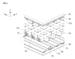
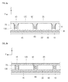
- a plasma display panel includes a first substrate (hereinafter, referred to as rear substrate) 10, a second substrate (hereinafter, referred to as front substrate) 20, a rear barrier layer 30, a front barrier layer 55, first display (Y) electrodes 70, second display (X) electrodes 80, and address (A) electrodes 60.
- the rear barrier layer 30 includes first barriers 30' and delimits a number of discharge cells 90.
- the front barrier layer 55 includes second barriers 40 and third barriers 50.
- First, second, and third fluorescent substance layers 110, 120, 130 are formed on the first, second, and third barriers 30', 40, 50, respectively.
- the discharge cells 90 are provided with fluorescent substance layers for absorbing vacuum UV rays and emitting visible rays and are filled with discharge gas for generating vacuum UV rays by means of plasma discharge.
- the rear substrate 10 is made of a predetermined material (e.g. glass) with a predetermined thickness and constitutes a plasma display panel together with the front substrate 20.
- the rear substrate 10 includes address electrodes 60 positioned in a predetermined direction on its upper surface, which opposes the front substrate 20, a first dielectric substance layer 45 applied so as to cover the address electrodes 60, and a rear barrier layer 30 (including first barriers 30') formed on top of the first dielectric substance layer 45.
- the rear barrier layer 30 may be solely composed of first barriers 30'. Alternatively, the rear barrier layer 30 may include another barrier layer in addition to first barriers 30'.
- a first fluorescent substance layer 110 is formed on the rear barrier layer 30.
- surfaces of components facing the front substrate 20 i.e. +z direction in FIG. 1 will be defined as upper surfaces and those facing the rear substrate 10 (i.e. -z direction in FIG. 1) will be defined as lower surfaces.
- the front substrate 20 is made of a transparent material (e.g. soda glass) and is positioned to oppose the rear substrate 10.
- the front substrate 20 has a front barrier layer 55 formed on its lower surface.
- the rear barrier layer 30 has a plurality of barriers 30' positioned therein in a predetermined direction (y direction in FIG. 1) while being substantially parallel to one another.
- the rear barrier layer 30 is of a stripe type, which is open in a direction (y direction in FIG. 1) and closed in another direction (x direction in FIG. 1).
- address discharge is initiated between lower portions of the first display electrodes 70 and upper portions of the address electrodes 60. Specifically, discharges occur first in regions where both electrodes are adjacent to each other and then spreads towards farther regions. If the first barriers 30' constituting the rear barrier layer 30 are of a closed type, application area of fluorescent substances increases and conversion efficiency into visible rays improves using the same UV generation efficiency.
- the present invention uses stripe-type barriers, instead of closed-type barriers which raise address discharge voltage, to lower address discharge voltage and reduce cost for address driving circuits.
- the rear barrier layer 30 delimits a number of discharge cells 90, which act as places for generating discharge together with the rear substrate 10, the front substrate 20, and the front barrier layer 55.
- the first barriers 30' are positioned substantially parallel to one another about the discharge cells 90 and have address electrodes 60 positioned therein while being substantially parallel to one another.
- the rear barrier layer 30 is made of glass including elements, such as Pb, B, Si, Al, and O.
- the rear barrier layer 30 is made of a dielectric substance including filler, such as zirconium oxide (ZrO 2 ), titanium oxide (TiO 2 ), or aluminum oxide (Al 2 O 3 ), and pigment, such as chromium (Cr), copper (Cu), cobalt (Co), or iron (Fe).
- the composition of the rear barrier layer 30 is not limited to that herein, and other dielectric substances may be used.
- the rear barrier layer 30 facilitates discharge of the address electrodes 60 positioned therein and prevents them from being damaged due to collision with charged particles which are accelerated during discharge.
- the front barrier layer 55 includes closed-type second barriers 40 for delimiting discharge cells 90 and closed-type third barriers 50 corresponding to the second barriers 40 to delimit discharge cells 90 with the first display electrodes and second display electrodes 70, 80 positioned therein.
- the front barrier layer 55 is of a closed-type.
- fluorescent substances can be applied in a larger area than in the case of a stripe-type barrier structure. This means that the closed-type barrier structure has better emission efficiency than the stripe-type barrier structure, provided that the electrode structure is the same.
- the front barrier layer 55 has a large fluorescent substance application area and realizes high visible ray conversion efficiency.
- the front barrier layer 55 delimits discharge cells 90 together with the rear barrier layer 30, when the rear substrate 10 is coupled to the front substrate 20.
- the front barrier layer 55 may be formed as a single unit with the front substrate 20 by etching it Alternatively, the front barrier layer 55 may be separately formed using a barrier material.
- the front barrier layer 55 may be made of a dielectric substance, as in the case of the rear barrier layer 30. In this case, the front barrier layer 55 may have a protective layer formed on its outer surface using magnesium oxide (MgO).
- MgO magnesium oxide
- the second barriers 40 are positioned on the lower surface of the front substrate 20 while making contact with it
- a second fluorescent substance layer 120 is formed on the outer surface of the second barriers 40 and on parts of the front substrate 20 having no second barrier 40 formed thereon.
- the second barriers 40 are of a closed type.
- the second barriers may be of a stripe-type.
- the second barrier 48 may be formed substantially parallel to y-axis direction in a shape corresponding to that of the first barriers 30.
- the third barriers 50 are formed on the lower surface of the second barriers 40 while contacting them.
- the third barriers 50 constitute the front barrier layer 55 together with the second barriers 40.
- the first display electrodes and second display electrodes 70, 80 are positioned inside the third barriers 50.
- the third barriers 50 have a third fluorescent substance layer 130 formed on lateral surfaces thereof
- the second and third barriers 40, 50 may be formed in a direction substantially parallel to the front substrate 20 in a sectional shape selected from a square, a hexagon, and a circle, but the shape is not limited to that herein.
- the first display electrodes and second display electrodes 70, 80 are positioned inside the third barriers 50 while alternating with each other about the discharge cells 90 and are shaped by adjacent discharge cells 90, respectively.
- the first display electrodes and second display electrodes 70, 80 are positioned in a direction (x direction in FIG. 1) perpendicular to the first barriers 30', which constitute the rear barrier layer 30, while being substantially parallel to each other.
- the first display electrodes and second display electrodes 70, 80 constitute pairs while opposing each other about the discharge cells 90, respectively, and conduct discharge. Therefore, the first display electrodes and second display electrodes 70, 80 may be spaced substantially the same distance from the front substrate 20 while facing each other.
- the first display electrodes and second display electrodes 70, 80 may be made of conventional conductive metal, because they are positioned inside the third barriers 50 and have no need for transparency.
- the first display electrodes and second display electrodes 70, 80 are made of a metallic material having excellent conductivity and low resistance, such as silver (Ag), aluminum (Al), or copper (Cu), in order to obtain fast response rate to discharge, avoid signal distortion, and decrease power consumption necessary for sustain discharge.
- material of the first display electrodes and second display electrodes 70, 80 is not limited to that herein, and any metal having excellent conductivity and low resistance may be used.
- the address electrodes 60 intersect with the first display electrodes and second display electrodes 70, 80 while being insulated from them.
- the address electrodes 60 are positioned on the rear substrate 10 while being substantially parallel to one another. In an exemplary embodiment, the address electrodes 60 approximately pass through the lower center of the discharge cells 90.
- the address electrodes 60 are entirely covered with the first dielectric substance layer 45. Particularly, the first dielectric substance layer 45 is positioned on the entire upper surface of the rear substrate 10 to cover the address electrodes 60. The first dielectric substance layer 45 facilitates discharge of the address electrodes 60 positioned on the upper surface of the rear substrate 10 and prevents them from being damaged due to collision with charged particles which are accelerated during discharge.
- the fluorescent substance layers 110, 120, 130 include a first fluorescent substance layer 110 formed on the lateral surfaces of the rear barrier layer 30 inside the discharge cells 90, a second fluorescent substance layer 120 formed on the lower surface of the front substrate 20 and on the lateral surfaces of the second barriers 40, and a third fluorescent substance layer 130 formed on the lateral surfaces of the third barriers.
- the first and third fluorescent substance layers 110, 130 absorb vacuum UV rays and generate visible rays, which are reflected towards the front substrate 20. Therefore, the first and third fluorescent substance layers 110, 130 are made of a reflective fluorescent substance.
- the second fluorescent substance layer 120 absorbs vacuum UV rays and transmits visible rays towards the front substrate 20.
- the second fluorescent substance layer 120 transmits visible rays, which are reflected by the first and third fluorescent substance layers 110, 130.
- the thickness of the second fluorescent substance layer 120 which is made of a transmissive fluorescent substance, is preferably smaller than that of the first and third fluorescent substance layers 110, 130, which are made of a reflective fluorescent substance.
- the transmissivity of visible rays in the second fluorescent substance layer 120 is inversely proportional to the thickness of the fluorescent substance layer. Therefore, the thickness of the second fluorescent substance layer 120 is properly determined based on the emission efficiency of the discharge cells.
- the first and third fluorescent substance layers 110, 130 reflect visible rays and must have a large thickness, in consideration of the emission efficiency of the discharge cells.
- the fluorescent substance layers 110, 120, 130 include components for receiving UV rays and generating visible rays.
- a red fluorescent substance layer formed on red emission discharge cells may include a fluorescent substance, such as Y(V,P)O 4 :Eu
- a green fluorescent substance layer formed on green emission discharge cells may includes a fluorescent substance, such as Zn 2 SiO 4 :Mn
- a blue fluorescent substance layer formed on blue emission discharge cells may include a fluorescent substance, such as BAM:Eu.
- the fluorescent substance layers 110, 120, 130 include red, green, and blue emission substance layers, which are positioned inside adjacent discharge cells 90, respectively. Therefore, adjacent discharge cells 90 are combined to constitute a unit pixel with red, green, and blue emission fluorescent layers formed thereon, respectively, and realize color images.
- the discharge cells 90 are delimited by the first dielectric substance layer 45 on the upper surface of the rear substrate 10, the rear barrier layer 30, the front barrier layer 55, and the front substrate 20.
- the discharge cells 90 are filled with discharge gas, e.g. mixture gas including xenon (Xe) and neon (Ne), to generate plasma discharge therein.
- the discharge cells 90 have fluorescent substance layers 110,120,130 formed in predetermined regions thereof to absorb UV rays and emit visible rays, as mentioned above.
- the width or length of the discharge cells 90 may vary depending on the emission efficiency of the respective fluorescent substance layers.
- the discharge cells 90 have electrodes positioned on their central and lower portions to conduct address discharge and sustain discharge.
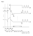
- FIG. 4 shows driving waves in a discharge process of a plasma display panel according to an embodiment of the present invention.
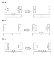
- FIGs. 5a to 5g show the distribution of wall charges based on driving waves according to embodiments of the present invention, respectively.
- address electrodes will be referred to as A electrodes, first display electrodes as Y electrodes, and second display electrodes as X electrodes.
- each sub-field includes a reset period, an address period, and a sustain period.
- the reset period is divided into an erasing period I , a Y electrode rising wave period II, and a Y electrode falling wave period III.
- erasing period I wall charges, which have been formed in a previous sustain discharge period, are erased. It is assumed in the present embodiment that sustain discharge voltage pulses are applied to the X electrodes near the end of the sustain discharge period, and a lower voltage (e.g. ground voltage) is applied to the Y electrodes than is applied to the X electrodes. Then, (+) wall charges are formed on the Y and A electrodes and (-) wall charges are formed on the X electrodes, as shown in FIG. 5a.
- ramp waves which gradually fall from voltage V a to ground voltage, are applied to the Y electrodes while biasing the X and A electrodes with ground voltage. Then, wall charges, which have been formed in the sustain discharge period, are erased.
- Y electrode falling wave period III ramp waves, which gradually fall from voltage V e to ground voltage, are applied to the Y electrodes while biasing the X and A electrodes with voltage V d and ground voltage, respectively.
- Slight reset discharge occurs in every discharge cell while the ramp waves fall.
- the Y electrode falling wave period is aimed to gradually reduce wall charges, which have accumulated in the Y electrode rising wave period. Therefore, the longer the falling wave time is (i.e. gentler the slope is), the better for address discharge, because reduction in wall charges can be controlled more precisely.
- a scan voltage is successively applied to the Y electrodes to apply scan pulses while biasing a number of X electrodes with voltage V d .
- an address voltage is applied to cells which need discharge.
- the scan pluses applied to the first display electrodes include negative first voltages V f and negative second voltages V g having an amplitude larger than that of the first voltages V f and alternating with them at a predetermined interval.
- the first voltages V f are applied, as shown in FIG. 5d, trigger discharge occurs between the Y electrodes of V f and the A electrodes of V 1 .
- the second voltages V g are applied, as shown in FIG.
- main discharge occurs between the Y electrodes of V g and the X electrodes of V d .
- the second voltages V g are applied to the Y electrodes, already-occurred trigger discharge is dispersed and main discharge occurs between V g applied to the Y electrodes and V d applied to the X electrodes.
- scan pulses are applied such that the first voltages and the second voltages V f , V g are successively applied only in the voltage rising period, and the second voltages V g fall to ground voltage in the voltage falling period. This is for the purpose of minimizing the address period and increasing the sustain period for luminance improvement
- sustain pulses are alternately applied to the Y and X electrodes while biasing a number of A electrodes with ground voltage.
- positive third voltages V h and positive fourth voltages V i having an amplitude larger than the third voltages alternative with each other at a predetermined interval.
- the third voltages V h are applied, as shown in FIG. 5f, trigger discharge occurs between the Y electrodes (V h ) and the A electrodes (ground voltage).
- the fourth voltages V i are applied, as shown in FIG. 5g, main discharge occurs between the Y electrodes (V i ) and the X electrodes (ground voltage).
- sustain pulses may be applied such that, in the voltage rising period, the third voltages and the fourth voltages V h , V i are successively applied and, in the voltage falling period, the fourth voltages and the third voltages V i , V h are successively applied, in contrast to the address period, so that the voltage rising period are linearly symmetric to the voltage falling period.
- discharge is performed such that, in early stages of the address and sustain periods, trigger discharge occurs between the Y and A electrodes so that discharge can be conducted even if initial particle number is small and, in a normal condition, main discharge occurs between the Y and X electrodes for stable discharge.
- the plasma display panel according to the present invention is advantageous in that stripe-type barriers are formed on the upper portion of the rear substrate in an opposite discharge structure to reduce the distance between the first display electrodes and the address electrodes and lower the address discharge voltage.
- multi-stage pulses are applied in the address and sustain periods to utilize trigger discharge and lower the sustain discharge voltage. This saves power consumption and improves emission efficiency.
- the present invention can use semiconductor devices having low nominal voltage to reduce manufacturing cost.
Landscapes
- Engineering & Computer Science (AREA)
- Physics & Mathematics (AREA)
- Plasma & Fusion (AREA)
- Chemical & Material Sciences (AREA)
- Materials Engineering (AREA)
- Power Engineering (AREA)
- Computer Hardware Design (AREA)
- General Physics & Mathematics (AREA)
- Theoretical Computer Science (AREA)
- Gas-Filled Discharge Tubes (AREA)
Applications Claiming Priority (1)
| Application Number | Priority Date | Filing Date | Title |
|---|---|---|---|
| KR1020050065858A KR100914111B1 (ko) | 2005-07-20 | 2005-07-20 | 플라즈마 디스플레이 패널 |
Publications (2)
| Publication Number | Publication Date |
|---|---|
| EP1746624A2 true EP1746624A2 (de) | 2007-01-24 |
| EP1746624A3 EP1746624A3 (de) | 2007-08-08 |
Family
ID=37137570
Family Applications (1)
| Application Number | Title | Priority Date | Filing Date |
|---|---|---|---|
| EP06117106A Withdrawn EP1746624A3 (de) | 2005-07-20 | 2006-07-13 | Plasma-Bildschirm |
Country Status (3)
| Country | Link |
|---|---|
| US (1) | US7710355B2 (de) |
| EP (1) | EP1746624A3 (de) |
| KR (1) | KR100914111B1 (de) |
Cited By (1)
| Publication number | Priority date | Publication date | Assignee | Title |
|---|---|---|---|---|
| EP2174333A4 (de) * | 2007-07-05 | 2010-08-04 | Lg Electronics Inc | Plasmaanzeigeschirm und plasmaanzeigevorrichtung |
Families Citing this family (1)
| Publication number | Priority date | Publication date | Assignee | Title |
|---|---|---|---|---|
| KR20090008609A (ko) * | 2007-07-18 | 2009-01-22 | 삼성에스디아이 주식회사 | 외광 반사 저감을 위한 격벽 및 이를 구비하는 플라즈마디스플레이 패널 |
Family Cites Families (19)
| Publication number | Priority date | Publication date | Assignee | Title |
|---|---|---|---|---|
| US5150007A (en) * | 1990-05-11 | 1992-09-22 | Bell Communications Research, Inc. | Non-phosphor full-color plasma display device |
| US5714840A (en) * | 1995-03-07 | 1998-02-03 | Asahi Glass Company Ltd. | Plasma display panel |
| US6008582A (en) * | 1997-01-27 | 1999-12-28 | Dai Nippon Printing Co., Ltd. | Plasma display device with auxiliary partition walls, corrugated, tiered and pigmented walls |
| JP3424587B2 (ja) * | 1998-06-18 | 2003-07-07 | 富士通株式会社 | プラズマディスプレイパネルの駆動方法 |
| JP3556097B2 (ja) * | 1998-06-30 | 2004-08-18 | 富士通株式会社 | プラズマディスプレイパネル駆動方法 |
| JP3201603B1 (ja) * | 1999-06-30 | 2001-08-27 | 富士通株式会社 | 駆動装置、駆動方法およびプラズマディスプレイパネルの駆動回路 |
| AU2001257111A1 (en) * | 2000-04-20 | 2001-11-07 | James C. Rutherford | Method for driving plasma display panel |
| JP4768134B2 (ja) * | 2001-01-19 | 2011-09-07 | 日立プラズマディスプレイ株式会社 | プラズマディスプレイ装置の駆動方法 |
| JP4205865B2 (ja) * | 2001-02-13 | 2009-01-07 | 株式会社日立製作所 | Ac型プラズマディスプレイ装置 |
| JP4158875B2 (ja) * | 2001-03-30 | 2008-10-01 | 株式会社日立プラズマパテントライセンシング | Ac型pdpの駆動方法および駆動装置 |
| WO2003032356A1 (en) * | 2001-10-02 | 2003-04-17 | Noritake Co., Limited | Gas discharge display device and its manufacturing method |
| JP3753171B2 (ja) * | 2002-03-18 | 2006-03-08 | 株式会社日立プラズマパテントライセンシング | プラズマディスプレイパネルおよびその製造方法 |
| KR100699337B1 (ko) * | 2002-11-25 | 2007-03-26 | 가부시키가이샤 티티티 | Ac형 pdp의 구조 |
| KR100647588B1 (ko) | 2003-10-29 | 2006-11-17 | 삼성에스디아이 주식회사 | 플라즈마 디스플레이 패널 및 이를 구비한 평판 표시 장치 |
| KR100625997B1 (ko) * | 2004-04-09 | 2006-09-20 | 삼성에스디아이 주식회사 | 플라즈마 디스플레이 패널 |
| KR20050101432A (ko) * | 2004-04-19 | 2005-10-24 | 삼성에스디아이 주식회사 | 플라즈마 디스플레이 패널의 제조방법 |
| KR20050101427A (ko) * | 2004-04-19 | 2005-10-24 | 삼성에스디아이 주식회사 | 플라즈마 디스플레이 패널 |
| US7649318B2 (en) * | 2004-06-30 | 2010-01-19 | Samsung Sdi Co., Ltd. | Design for a plasma display panel that provides improved luminance-efficiency and allows for a lower voltage to initiate discharge |
| KR100669465B1 (ko) | 2005-02-24 | 2007-01-15 | 삼성에스디아이 주식회사 | 플라즈마 디스플레이 패널 및 그 구동방법 |
-
2005
- 2005-07-20 KR KR1020050065858A patent/KR100914111B1/ko not_active Expired - Fee Related
-
2006
- 2006-07-13 EP EP06117106A patent/EP1746624A3/de not_active Withdrawn
- 2006-07-19 US US11/489,930 patent/US7710355B2/en not_active Expired - Fee Related
Non-Patent Citations (1)
| Title |
|---|
| None |
Cited By (2)
| Publication number | Priority date | Publication date | Assignee | Title |
|---|---|---|---|---|
| EP2174333A4 (de) * | 2007-07-05 | 2010-08-04 | Lg Electronics Inc | Plasmaanzeigeschirm und plasmaanzeigevorrichtung |
| US8031138B2 (en) | 2007-07-05 | 2011-10-04 | Lg Electronics Inc. | Plasma display panel and plasma display apparatus |
Also Published As
| Publication number | Publication date |
|---|---|
| KR20070010881A (ko) | 2007-01-24 |
| US7710355B2 (en) | 2010-05-04 |
| EP1746624A3 (de) | 2007-08-08 |
| KR100914111B1 (ko) | 2009-08-27 |
| US20070171174A1 (en) | 2007-07-26 |
Similar Documents
| Publication | Publication Date | Title |
|---|---|---|
| US7471044B2 (en) | Plasma display panel having an address electrode including loop shape portions | |
| US7710355B2 (en) | Plasma display panel | |
| US7327084B2 (en) | Plasma display panel | |
| EP1715502B1 (de) | Plasmaanzeigetafel | |
| US20060125395A1 (en) | Plasma display panel | |
| KR100573112B1 (ko) | 플라즈마 디스플레이 패널 | |
| KR100719552B1 (ko) | 플라즈마 디스플레이 패널 | |
| KR100731460B1 (ko) | 플라즈마 디스플레이 패널 | |
| CN101527242A (zh) | 等离子体显示面板 | |
| KR100686836B1 (ko) | 플라즈마 디스플레이 패널 | |
| KR100581944B1 (ko) | 플라즈마 디스플레이 패널 | |
| KR100637232B1 (ko) | 플라즈마 디스플레이 패널 | |
| KR100659074B1 (ko) | 플라즈마 디스플레이 패널 | |
| KR100592311B1 (ko) | 플라즈마 디스플레이 패널 | |
| KR100696804B1 (ko) | 대향방전 전극을 갖는 플라즈마 디스플레이 패널의구동방법 | |
| KR100615333B1 (ko) | 플라즈마 디스플레이 패널 | |
| KR100581955B1 (ko) | 플라즈마 디스플레이 패널 | |
| KR100879470B1 (ko) | 플라즈마 디스플레이 패널 | |
| KR100741123B1 (ko) | 플라즈마 디스플레이 패널 | |
| KR100730128B1 (ko) | 플라즈마 디스플레이 패널 | |
| KR100659109B1 (ko) | 플라즈마 디스플레이 패널 | |
| KR100846602B1 (ko) | 플라즈마 디스플레이 패널 | |
| KR100615322B1 (ko) | 플라즈마 디스플레이 패널 | |
| US20070152590A1 (en) | Plasma display panel | |
| US20070007886A1 (en) | Plasma display panel |
Legal Events
| Date | Code | Title | Description |
|---|---|---|---|
| PUAI | Public reference made under article 153(3) epc to a published international application that has entered the european phase |
Free format text: ORIGINAL CODE: 0009012 |
|
| 17P | Request for examination filed |
Effective date: 20060713 |
|
| AK | Designated contracting states |
Kind code of ref document: A2 Designated state(s): AT BE BG CH CY CZ DE DK EE ES FI FR GB GR HU IE IS IT LI LT LU LV MC NL PL PT RO SE SI SK TR |
|
| AX | Request for extension of the european patent |
Extension state: AL BA HR MK YU |
|
| PUAL | Search report despatched |
Free format text: ORIGINAL CODE: 0009013 |
|
| AK | Designated contracting states |
Kind code of ref document: A3 Designated state(s): AT BE BG CH CY CZ DE DK EE ES FI FR GB GR HU IE IS IT LI LT LU LV MC NL PL PT RO SE SI SK TR |
|
| AX | Request for extension of the european patent |
Extension state: AL BA HR MK YU |
|
| RIC1 | Information provided on ipc code assigned before grant |
Ipc: G09G 3/28 20060101ALI20070629BHEP Ipc: H01J 17/16 20060101ALI20070629BHEP Ipc: H01J 17/04 20060101AFI20061114BHEP |
|
| AKX | Designation fees paid |
Designated state(s): DE FR GB |
|
| 17Q | First examination report despatched |
Effective date: 20081021 |
|
| RIC1 | Information provided on ipc code assigned before grant |
Ipc: G09G 3/28 20060101ALI20100331BHEP Ipc: H01J 17/16 20060101ALI20100331BHEP Ipc: H01J 17/04 20060101AFI20100331BHEP |
|
| GRAP | Despatch of communication of intention to grant a patent |
Free format text: ORIGINAL CODE: EPIDOSNIGR1 |
|
| STAA | Information on the status of an ep patent application or granted ep patent |
Free format text: STATUS: THE APPLICATION IS DEEMED TO BE WITHDRAWN |
|
| 18D | Application deemed to be withdrawn |
Effective date: 20101217 |