EP1746746A1 - Émetteur optique avec générateur de distorsion préalable - Google Patents
Émetteur optique avec générateur de distorsion préalable Download PDFInfo
- Publication number
- EP1746746A1 EP1746746A1 EP05291545A EP05291545A EP1746746A1 EP 1746746 A1 EP1746746 A1 EP 1746746A1 EP 05291545 A EP05291545 A EP 05291545A EP 05291545 A EP05291545 A EP 05291545A EP 1746746 A1 EP1746746 A1 EP 1746746A1
- Authority
- EP
- European Patent Office
- Prior art keywords
- feed forward
- signal
- optical
- optical signal
- modulator
- Prior art date
- Legal status (The legal status is an assumption and is not a legal conclusion. Google has not performed a legal analysis and makes no representation as to the accuracy of the status listed.)
- Withdrawn
Links
- 230000003287 optical effect Effects 0.000 title claims abstract description 40
- 230000005540 biological transmission Effects 0.000 claims abstract description 35
- 239000006185 dispersion Substances 0.000 claims abstract description 11
- 238000012546 transfer Methods 0.000 claims description 4
- 238000010586 diagram Methods 0.000 description 6
- 230000003111 delayed effect Effects 0.000 description 3
- 238000013461 design Methods 0.000 description 3
- 239000000835 fiber Substances 0.000 description 3
- 238000001997 free-flow electrophoresis Methods 0.000 description 3
- 230000001934 delay Effects 0.000 description 2
- 238000011161 development Methods 0.000 description 2
- 230000003068 static effect Effects 0.000 description 2
- 238000011144 upstream manufacturing Methods 0.000 description 2
- 238000013459 approach Methods 0.000 description 1
- 238000004891 communication Methods 0.000 description 1
- 230000001419 dependent effect Effects 0.000 description 1
- 230000000694 effects Effects 0.000 description 1
- 238000003780 insertion Methods 0.000 description 1
- 230000037431 insertion Effects 0.000 description 1
- 230000008054 signal transmission Effects 0.000 description 1
Images

Classifications
-
- H—ELECTRICITY
- H04—ELECTRIC COMMUNICATION TECHNIQUE
- H04B—TRANSMISSION
- H04B10/00—Transmission systems employing electromagnetic waves other than radio-waves, e.g. infrared, visible or ultraviolet light, or employing corpuscular radiation, e.g. quantum communication
- H04B10/50—Transmitters
- H04B10/501—Structural aspects
- H04B10/503—Laser transmitters
- H04B10/505—Laser transmitters using external modulation
-
- H—ELECTRICITY
- H04—ELECTRIC COMMUNICATION TECHNIQUE
- H04B—TRANSMISSION
- H04B10/00—Transmission systems employing electromagnetic waves other than radio-waves, e.g. infrared, visible or ultraviolet light, or employing corpuscular radiation, e.g. quantum communication
- H04B10/25—Arrangements specific to fibre transmission
- H04B10/2507—Arrangements specific to fibre transmission for the reduction or elimination of distortion or dispersion
- H04B10/2513—Arrangements specific to fibre transmission for the reduction or elimination of distortion or dispersion due to chromatic dispersion
- H04B10/25137—Arrangements specific to fibre transmission for the reduction or elimination of distortion or dispersion due to chromatic dispersion using pulse shaping at the transmitter, e.g. pre-chirping or dispersion supported transmission [DST]
-
- H—ELECTRICITY
- H04—ELECTRIC COMMUNICATION TECHNIQUE
- H04B—TRANSMISSION
- H04B10/00—Transmission systems employing electromagnetic waves other than radio-waves, e.g. infrared, visible or ultraviolet light, or employing corpuscular radiation, e.g. quantum communication
- H04B10/50—Transmitters
- H04B10/501—Structural aspects
- H04B10/503—Laser transmitters
- H04B10/505—Laser transmitters using external modulation
- H04B10/5059—Laser transmitters using external modulation using a feed-forward signal generated by analysing the optical or electrical input
- H04B10/50593—Laser transmitters using external modulation using a feed-forward signal generated by analysing the optical or electrical input to control the modulating signal amplitude including amplitude distortion
-
- H—ELECTRICITY
- H04—ELECTRIC COMMUNICATION TECHNIQUE
- H04B—TRANSMISSION
- H04B10/00—Transmission systems employing electromagnetic waves other than radio-waves, e.g. infrared, visible or ultraviolet light, or employing corpuscular radiation, e.g. quantum communication
- H04B10/50—Transmitters
- H04B10/508—Pulse generation, e.g. generation of solitons
Definitions
- the invention relates to a device for transmitting an optical signal via an optical transmission link, which induces chromatic dispersion of the optical signal, the device comprising filter means for predistorting the optical signal in accordance with an input signal for the filter means prior to its transmission via the optical transmission link.
- Chromatic, i.e. wavelength-dependent dispersion compensation is a key issue for the design and operation of transmission systems with data rates of 10 Gb/s and beyond.
- a dispersion compensation fiber DCF
- CD chromatic dispersion
- More and more, systems without any chromatic dispersion (CD) compensation therefore are of interest for metro applications with overall system lengths ranging up to several hundreds of kilometers.
- an electronic equaliser analog or digital
- suitable modulation formats in combination with prechirped signals lead to an additional extension of the system range.
- the most flexible solution achieving the longest reach is a system which transmits a predistorted signal in order to cope with the effects of CD.
- Prior art document WO 2004/032385 A1 discloses an optical communication system for transmitting predistorted optical signals, wherein signal predistorsion is based on the calculation of magnitude and phase of real part and imaginary part of a transmitted signal by means of a digital signal processor (DSP) with a high degree of complexity.
- DSP digital signal processor
- a predistorted signal is determined in the digital domain using look-up tables or digital filters.
- the predistorted signal is then fed to a digital-to-analog (D/A) converter, which generates a corresponding analog signal.
- the analog signal is subsequently fed to a modulator, which enables separate modulation of the optical signal with respect to its magnitude and phase.
- filter means comprise at least one feed forward equaliser (FFE), i.e. a FIR (finite impulse response) non-recursive filter.
- FFE feed forward equaliser
- the invention leads to a drastic reduction of realisation complexity for a transmission system involving signal predistorsion. For instance, use of a DSP with a very high number of data outputs is no longer necessary. The same holds for the use of a D/A converter with high resolution. The reduced complexity in turn entails lower costs per system and savings in terms of power consumption.
- the input signal is a digital signal, i.e. a sequence of noise free binary data bits with a predetermined bit period comprising data to be transmitted via the optical transmission link by means of the optical signal.
- the digital input signal is delayed in a series of delay stages, i.e. digital delay means in the form of a so-called FIR tapped delay line.
- each of the digital delay means has a delay of exactly one bit period of the input signal and a pure digital signal in forward path.
- Such delay means are commonly known as unit delays.
- the realisation of the delay stages as purely digital delay means contributes to the overall simplified and improved structure of the inventive device by providing a highly simplified delay structure without any signal distortion. This obviates the common disadvantage of high bit-rate FFEs with respect to signal distortion in the forward path, on which the signal is delayed by several bit periods.
- the feed forward equaliser comprises analog multiplying and adding means, whereas all other components are digital elements.
- multipliers and adding means can easily be implemented as analog functional elements with high performance.
- the feed forward equaliser provides an output signal usable for driving a modulator for modulating the optical signal.
- the FFE of the inventive device thus operates as a predistorsion preprocessor whose output signal can be used directly for driving the modulator, e.g. either its modulation magnitude or phase if only one FFE is used, which "imprints" the data to be sent on an optical carrier wave using a convenient coding scheme, such as RZ, NRZ, or the like.
- the filter means may comprise two feed forward equalisers in parallel connection.
- the two FFEs will then operate in parallel with subsequent multiplexing.
- the feed forward equaliser may comprise delay means each having a delay of a fraction of one bit period of the input signal, i.e. a fractionally spaced FFE, which is sampled for instance at T/2 or T/3, T being the bit period.
- the feed forward equaliser in the inventive device i.e.
- the filter means can comprise a tapped delay line with a number of weighted taps in connection with a common adding means, at least two of said taps, e.g. indexed i and j, being in connection with a transfer means, in particular a logic circuit such as an AND-gate, arranged in weighted connection (weighting value c i-j ) with said adding means.
- a transfer means in particular a logic circuit such as an AND-gate, arranged in weighted connection (weighting value c i-j ) with said adding means.
- the tap weighting values are supplied by value delivery means for determining and delivering values for weighting contributions of the input signal in the feed forward equaliser.
- the number of taps i.e. the quantity n introduced above, is determined by the dispersion of the transmission medium itself, e.g. an optical waveguide fiber.
- an analog circuit element is arranged between and in connection with both the feed forward equaliser and a modulator for modulating the optical signal, said analog circuit element having an inverse transmission function for an output signal of the feed forward equaliser with respect to a corresponding transmission function of said modulator and/or a driver circuit for said modulator.
- the modulator usually requires a driver means with high output voltages. Such drivers generally suffer from inherent distortions which can be balanced by means of the aforementioned inverse non-linear analog circuit, too.
- Fig. 1 shows a general transmission system 1 for an optical signal OS.
- the system 1 comprises a device 2 for transmitting the optical signal OS according to the invention, hereinafter also referred to as a transmitter, and a receiver 3 for receiving the optical signal OS.
- the transmitter 2 and the receiver 3 are connected by means of a transmission link 4, e.g. an optical waveguide fiber, which is adapted for transmission of the optical signal OS and which is generally subject to chromatic dispersion of the transmitted optical signal OS.
- the receiver 2 comprises an input pin 5 for a digital input signal IN in operative connection with filter means 6, the design of which will be described in greater detail hereinafter.
- the filter means 6 is also connected with a modulator 7 for modulating a suitable light wave emitted by a light source, e.g.
- the system 1 furthermore comprises a value delivery means 8 for determining and/or delivering tap weighting values in operative connection with the filter means 6, whose function and design will also be described in more detail in the following.
- the value delivery means 8 is shown as a unit separate from the transmitter 2. However, it could also be designed as an integral part of the latter.
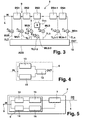
- Fig. 2 shows a detailed block diagram of the filter means 6 comprised in the inventive transmitter 2 according to a first embodiment.
- the filter means 6 is designed as a feed forward equaliser (FFE) comprising a delay line 9 for delaying a purely digital input data signal IN in a series of n digital delay stages DS1-DSn, commonly referred to as unit delays for delaying the input signal IN by one bit period each.
- FFE feed forward equaliser
- the delay stages DS1-DSn are realised in the form of purely digital delay stages arranged in the forward path of the input signal IN, e.g.
- the delay line 9 is tapped behind every delay stage DS1-DSn ("downstream" with respect to the signal input 5), e.g. behind each flip-flop in the case of a shift register, as well as "upstream" of the first delay stage DS1 by means of tap lines TL0-TLn, which are connected to a common analog adding means ADD.
- the adding means ADD has an output 10 for an output signal OUT of the feed forward equaliser.
- the output 10 is connected with the modulator 7 (cf. Fig. 1).
- the weighted contributions on every tap line TL0-TLn i.e.
- c 0 ⁇ x(t), c 1 ⁇ x(t-T),...,c n ⁇ x(t-n ⁇ T) are then fed to the adding means ADD for performing a summing operation, thus determining a predistorted signal in the form of the output signal OUT for directly driving the modulator 7 (cf. Fig. 1).
- the weighting values c 0 -c n are provided by the value delivery means 8 (cf. Fig. 1), which can be a digital processor or an analog circuitry, either by reading a stored look-up table or by feedback, e.g. from the receiver 3 (cf. Fig. 1), by means of a suitable feedback line (not shown).
- the filter means 6 comprise an additional signal transfer means in the form of a logic circuit element 11, in particular an AND-gate, which is arranged between and in operative connection with the tap lines TL2 and TL3 upstream of the corresponding multipliers MU2 and MU3, respectively.
- Downstream of the logic circuit element 11 in a corresponding additional tap line TL2-3 is included a corresponding additional multiplier MU2-3 for multiplying an output value of the logic circuit element 11 with a tap weight c 2-3 prior to summing in the adding means ADD.
- the output signal of the filter means 6 is compatible with a 10 Gb/s system 1.
- two feed forward equalisers according to the embodiments shown in Figs 2 and 3 may be arranged to operate in parallel, followed by a time domain multiplexer 12, as depicted in Fig. 4.
- a first feed forward equaliser 13 accounts for the even bit periods of the output signal OUT whereas a second feed forward equaliser 14 arranged in parallel connection with respect to the first FFE 13 provides the odd bit periods of the output signal OUT.
- the output signal is again used to drive the modulator 7.
- the delay stages DS1-DSn in a filter means 6 can be realised with spacings corresponding to half of the bit period T, i.e. with spacings equal to T/2, or other suitable fractions of the bit period T (not shown).
- Fig. 5 shows an embodiment of the inventive device 2 in which the filter means 6 again comprises two FFE structures 13, 14 arranged in parallel connection for driving a modulator 7, wherein one FFE 13 drives the modulator 7 with respect to the magnitude of modulation while the other FFE 14 drives the modulator 7 with respect to the modulation phase to generate the optical signal OS to be transmitted via transmission link 4.
- the modulator 7 generally has a non-linear transmission function for both analog and digital predistorsion generation, non-linear analog circuits 15, 16, respectively, have been inserted between each FFE 13, 14 and the modulator 7.
- the non-linear circuits 15, 16 are chosen to present an inverse non-linear transmission function compared with the modulator 7, thus making the overall transmission function of the arrangement fully linear.
- the modulator 7 generally requires a driver circuit (not shown) with higher output voltages. Such driver circuits also suffer from inherent distortion, which can be suppressed by means of the aforementioned non-linear circuits 15, 16, too.
- the transmission device allows the realisation of transmission systems, in particular optical data transmission systems, which are subject to chromatic dispersion of the transmitted signals, with drastically reduced system complexity, entailing reduced system costs with respect to hardware expenditure as well as power consumption.
Landscapes
- Physics & Mathematics (AREA)
- Electromagnetism (AREA)
- Engineering & Computer Science (AREA)
- Computer Networks & Wireless Communication (AREA)
- Signal Processing (AREA)
- Optics & Photonics (AREA)
- Optical Communication System (AREA)
Priority Applications (1)
| Application Number | Priority Date | Filing Date | Title |
|---|---|---|---|
| EP05291545A EP1746746A1 (fr) | 2005-07-19 | 2005-07-19 | Émetteur optique avec générateur de distorsion préalable |
Applications Claiming Priority (1)
| Application Number | Priority Date | Filing Date | Title |
|---|---|---|---|
| EP05291545A EP1746746A1 (fr) | 2005-07-19 | 2005-07-19 | Émetteur optique avec générateur de distorsion préalable |
Publications (1)
| Publication Number | Publication Date |
|---|---|
| EP1746746A1 true EP1746746A1 (fr) | 2007-01-24 |
Family
ID=35427428
Family Applications (1)
| Application Number | Title | Priority Date | Filing Date |
|---|---|---|---|
| EP05291545A Withdrawn EP1746746A1 (fr) | 2005-07-19 | 2005-07-19 | Émetteur optique avec générateur de distorsion préalable |
Country Status (1)
| Country | Link |
|---|---|
| EP (1) | EP1746746A1 (fr) |
Cited By (2)
| Publication number | Priority date | Publication date | Assignee | Title |
|---|---|---|---|---|
| WO2011146363A3 (fr) * | 2010-05-17 | 2012-01-12 | Neophotonics Corporation | Système de transport optique de réseau coaxial à fibre hybride avec régulation de distorsion |
| CN109391237A (zh) * | 2018-09-30 | 2019-02-26 | 西安空间无线电技术研究所 | 用于行波管功率放大器预失真的线性化器及其调节方法 |
Citations (4)
| Publication number | Priority date | Publication date | Assignee | Title |
|---|---|---|---|---|
| US4989212A (en) * | 1990-04-09 | 1991-01-29 | Trw, Inc. | Laser diode phase modulation technique |
| EP0938197A2 (fr) * | 1998-02-20 | 1999-08-25 | Lucent Technologies Inc. | Méthode et dispositif de communication à multiplexage en longeur d'onde de grande capacité avec des impulsions à période modulée |
| WO2004032385A1 (fr) | 2002-10-03 | 2004-04-15 | Nortel Networks Limited | Compensation de la dispersion optique dans le domaine electrique dans un systeme de communication optique |
| WO2004077111A2 (fr) * | 2003-02-27 | 2004-09-10 | Oplink Communications, Inc. | Transpondeur optique adaptatif |
-
2005
- 2005-07-19 EP EP05291545A patent/EP1746746A1/fr not_active Withdrawn
Patent Citations (4)
| Publication number | Priority date | Publication date | Assignee | Title |
|---|---|---|---|---|
| US4989212A (en) * | 1990-04-09 | 1991-01-29 | Trw, Inc. | Laser diode phase modulation technique |
| EP0938197A2 (fr) * | 1998-02-20 | 1999-08-25 | Lucent Technologies Inc. | Méthode et dispositif de communication à multiplexage en longeur d'onde de grande capacité avec des impulsions à période modulée |
| WO2004032385A1 (fr) | 2002-10-03 | 2004-04-15 | Nortel Networks Limited | Compensation de la dispersion optique dans le domaine electrique dans un systeme de communication optique |
| WO2004077111A2 (fr) * | 2003-02-27 | 2004-09-10 | Oplink Communications, Inc. | Transpondeur optique adaptatif |
Non-Patent Citations (1)
| Title |
|---|
| PELARD C ET AL: "Multilevel signaling and equalization over multimode fiber at 10 Gbit/s", GAAS IC SYMPOSIUM. 25TH. ANNUAL IEEE GALLIUM ARSENIDE INTEGRATED CIRCUIT SYMPOSIUM. TECHNICAL DIGEST 2003. SAN DIEGO, CA, NOV. 9 - 12, 2003, GAAS IC SYMPOSIUM - IEEE GALLIUM ARSENIDE INTEGRATED CIRCUIT SYMPOSIUM, NEW YORK, NY : IEEE, US, 9 November 2003 (2003-11-09), pages 197 - 199, XP010673659, ISBN: 0-7803-7833-4 * |
Cited By (4)
| Publication number | Priority date | Publication date | Assignee | Title |
|---|---|---|---|---|
| WO2011146363A3 (fr) * | 2010-05-17 | 2012-01-12 | Neophotonics Corporation | Système de transport optique de réseau coaxial à fibre hybride avec régulation de distorsion |
| US8867928B2 (en) | 2010-05-17 | 2014-10-21 | Neophotonics Corporation | Hybrid fiber coaxial network optical transport system with distortion control |
| US9369205B2 (en) | 2010-05-17 | 2016-06-14 | Neophotonics Corporation | Pluggable optical transmitter module for network optical transport system with distortion control |
| CN109391237A (zh) * | 2018-09-30 | 2019-02-26 | 西安空间无线电技术研究所 | 用于行波管功率放大器预失真的线性化器及其调节方法 |
Similar Documents
| Publication | Publication Date | Title |
|---|---|---|
| US5222084A (en) | Echo canceler having adaptive digital filter unit associated with delta-sigma modulation circuit | |
| CN102598541A (zh) | 预均衡光发送器以及预均衡光纤传送系统 | |
| US7880543B2 (en) | Data transmitting circuit and transmitting method | |
| US8139958B2 (en) | Frequency-domain equalization of the fiber optic channel | |
| KR100404012B1 (ko) | 적응성 비선형 에코 보상기 | |
| CN103460629A (zh) | 用于导频辅助的数据传输的相干光接收机 | |
| EP1538797B1 (fr) | Transmission électrique à fond de panier utilisant une signalisation duobinaire | |
| Fougstedt et al. | ASIC implementation of time-domain digital back propagation for coherent receivers | |
| US7321734B2 (en) | Digital synthesis of readily compensated optical signals | |
| EP1746746A1 (fr) | Émetteur optique avec générateur de distorsion préalable | |
| EP1579606A2 (fr) | Emetteur et procede utilisant des flux de donnees demi-vitesse aux fins de generation d'une modulation pleine vitesse sur un signal optique | |
| Winzer et al. | Electronic pre-distortion for advanced modulation formats | |
| JP2023010593A (ja) | ディストータ係数更新装置、方法及びデジタルプリディストーション装置 | |
| US20210152254A1 (en) | Method and apparatus for pre-distorting an input signal for an optical transmitter | |
| US20140269247A1 (en) | Method and apparatus to compensate for nonlinear echo in an output of a current source | |
| JP5116573B2 (ja) | 分散予等化光送信器 | |
| EP2095545A1 (fr) | Processeur de signaux destiné à compenser la dispersion chromatique de fibres optiques | |
| JP2020113832A (ja) | 光受信装置及び波形歪み補償方法 | |
| JP5991210B2 (ja) | 光信号送信装置 | |
| JP5713776B2 (ja) | 予等化光送信機 | |
| US20050201455A1 (en) | Equalizer architecture | |
| US10148464B1 (en) | Systems and methods for equalizing a laser drive signal | |
| Jiang et al. | Advances in SiGe ICs for 40Gb/s signal equalization | |
| CN115398827A (zh) | 用于补偿光传输系统中的群速度色散的数字滤波器装置 | |
| Iqbal et al. | Low power on-chip data transmission for wafer-scale monolithic active pixel sensors |
Legal Events
| Date | Code | Title | Description |
|---|---|---|---|
| PUAI | Public reference made under article 153(3) epc to a published international application that has entered the european phase |
Free format text: ORIGINAL CODE: 0009012 |
|
| AK | Designated contracting states |
Kind code of ref document: A1 Designated state(s): AT BE BG CH CY CZ DE DK EE ES FI FR GB GR HU IE IS IT LI LT LU LV MC NL PL PT RO SE SI SK TR |
|
| AX | Request for extension of the european patent |
Extension state: AL BA HR MK YU |
|
| RAP1 | Party data changed (applicant data changed or rights of an application transferred) |
Owner name: ALCATEL LUCENT |
|
| AKX | Designation fees paid | ||
| STAA | Information on the status of an ep patent application or granted ep patent |
Free format text: STATUS: THE APPLICATION IS DEEMED TO BE WITHDRAWN |
|
| 18D | Application deemed to be withdrawn |
Effective date: 20070725 |
|
| REG | Reference to a national code |
Ref country code: DE Ref legal event code: 8566 |