EP1748324A1 - Bildtrommel und ihr Herstellungsverfahren - Google Patents
Bildtrommel und ihr Herstellungsverfahren Download PDFInfo
- Publication number
- EP1748324A1 EP1748324A1 EP06011691A EP06011691A EP1748324A1 EP 1748324 A1 EP1748324 A1 EP 1748324A1 EP 06011691 A EP06011691 A EP 06011691A EP 06011691 A EP06011691 A EP 06011691A EP 1748324 A1 EP1748324 A1 EP 1748324A1
- Authority
- EP
- European Patent Office
- Prior art keywords
- electrodes
- semi
- cylindrical members
- substrate
- conductive parts
- Prior art date
- Legal status (The legal status is an assumption and is not a legal conclusion. Google has not performed a legal analysis and makes no representation as to the accuracy of the status listed.)
- Granted
Links
Images


Classifications
-
- B—PERFORMING OPERATIONS; TRANSPORTING
- B41—PRINTING; LINING MACHINES; TYPEWRITERS; STAMPS
- B41J—TYPEWRITERS; SELECTIVE PRINTING MECHANISMS, i.e. MECHANISMS PRINTING OTHERWISE THAN FROM A FORME; CORRECTION OF TYPOGRAPHICAL ERRORS
- B41J2/00—Typewriters or selective printing mechanisms characterised by the printing or marking process for which they are designed
- B41J2/385—Typewriters or selective printing mechanisms characterised by the printing or marking process for which they are designed characterised by selective supply of electric current or selective application of magnetism to a printing or impression-transfer material
- B41J2/39—Typewriters or selective printing mechanisms characterised by the printing or marking process for which they are designed characterised by selective supply of electric current or selective application of magnetism to a printing or impression-transfer material using multi-stylus heads
- B41J2/395—Structure of multi-stylus heads
-
- G—PHYSICS
- G03—PHOTOGRAPHY; CINEMATOGRAPHY; ANALOGOUS TECHNIQUES USING WAVES OTHER THAN OPTICAL WAVES; ELECTROGRAPHY; HOLOGRAPHY
- G03G—ELECTROGRAPHY; ELECTROPHOTOGRAPHY; MAGNETOGRAPHY
- G03G15/00—Apparatus for electrographic processes using a charge pattern
- G03G15/22—Apparatus for electrographic processes using a charge pattern involving the combination of more than one step according to groups G03G13/02 - G03G13/20
- G03G15/34—Apparatus for electrographic processes using a charge pattern involving the combination of more than one step according to groups G03G13/02 - G03G13/20 in which the powder image is formed directly on the recording material, e.g. by using a liquid toner
- G03G15/344—Apparatus for electrographic processes using a charge pattern involving the combination of more than one step according to groups G03G13/02 - G03G13/20 in which the powder image is formed directly on the recording material, e.g. by using a liquid toner by selectively transferring the powder to the recording medium, e.g. by using a LED array
- G03G15/348—Apparatus for electrographic processes using a charge pattern involving the combination of more than one step according to groups G03G13/02 - G03G13/20 in which the powder image is formed directly on the recording material, e.g. by using a liquid toner by selectively transferring the powder to the recording medium, e.g. by using a LED array using a stylus or a multi-styli array
-
- B—PERFORMING OPERATIONS; TRANSPORTING
- B41—PRINTING; LINING MACHINES; TYPEWRITERS; STAMPS
- B41J—TYPEWRITERS; SELECTIVE PRINTING MECHANISMS, i.e. MECHANISMS PRINTING OTHERWISE THAN FROM A FORME; CORRECTION OF TYPOGRAPHICAL ERRORS
- B41J2202/00—Embodiments of or processes related to ink-jet or thermal heads
- B41J2202/01—Embodiments of or processes related to ink-jet heads
- B41J2202/22—Manufacturing print heads
-
- G—PHYSICS
- G03—PHOTOGRAPHY; CINEMATOGRAPHY; ANALOGOUS TECHNIQUES USING WAVES OTHER THAN OPTICAL WAVES; ELECTROGRAPHY; HOLOGRAPHY
- G03G—ELECTROGRAPHY; ELECTROPHOTOGRAPHY; MAGNETOGRAPHY
- G03G2217/00—Details of electrographic processes using patterns other than charge patterns
- G03G2217/0075—Process using an image-carrying member having an electrode array on its surface
Definitions
- the present invention relates to an image forming apparatus. More particularly, the present invention relates to an image drum used for a direct printing method of an image forming apparatus and a manufacturing method thereof.
- a direct printing method is a method in which a predetermined drum is directly applied with an image signal, and a latent image is made and developed, and a visible image is formed.
- the direct printing method has a stable characteristic in processing and has been continuously studied.
- the operational principle of an image drum forming apparatus by a direct printing method is disclosed in EP 0 247 699 A1 , and a structure and manufacturing method of image drum are disclosed in EP 0 595 388 A1 and US 6,014,157 .
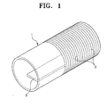
- FIG. 1 is a schematic representation illustrating an image forming element disclosed in US 6,014,157 .
- the image forming element includes a cylindrical drum body 1, a plurality of line electrodes 2 formed at a periphery of the drum body 1, and a control unit 3 mounted inside the drum body 1.
- the cylindrical drum body 1 is manufactured with aluminum or aluminum alloy.
- Each line electrode 2 is insulated from adjacent neighboring electrodes and also insulated from the drum body 1. Furthermore, each line electrode 2 is formed with a through hole (not shown), and the through hole is filled with a conductive material.
- the control unit 3 has a terminal, and the terminal and each line electrode 2 are electrically connected by zebra-strip.
- the control unit 3 applies an appropriate high voltage to each line electrode 2, and the image forming element is formed with a predetermined latent image by the applied high voltage.
- the image forming element thus described according to the prior art has a disadvantage in that its manufacturing process is complicated and the manufacturing cost is high.
- the image forming element needs a surface treatment, fine pattern processing by using a laser and E-beam, epoxy and dielectric layer coating, and a coating process by conductive particles.
- An aspect of the present invention is to provide an image drum and a manufacturing method thereof configured to simplify the manufacturing process and to save manufacturing cost.
- Another aspect of the present invention is to provide an image drum and a manufacturing method thereof configured to improve a connecting structure between a substrate comprising a control unit and a drum body connecting the substrate, thereby improving reliability.
- an image drum comprising a drum body made of a pair of semi-cylindrical members each oppositely bonded and formed at a bonding surface of the semi-cylindrical member with a plurality of mutually insulated electrodes and formed at a periphery thereof with line electrodes in the same gap as that of the electrode; a control unit including conductive parts corresponding to the line electrodes and a nonconductive part interposed between the conductive parts and disposed inside the drum body; and a connecting member electrically connecting each line electrode of the drum body to the substrate of the control unit.
- the connecting member may include metal bumps such as solder bumps each formed on the electrode of the semi-cylindrical member and a counter conductive part of the substrate.
- the connecting member may be made of anisotropic conductive films each attached to the electrode of the semi-cylindrical member and to a counter portion of the conductive part of the substrate.
- the drum body and the substrate may be made of aluminum or aluminum alloy.
- the conductive parts and the nonconductive part may be disposed between the conductive parts are formed by partial oxidation of the aluminum substrate.
- a image drum manufacturing method comprising cutting an aluminum cylindrical member into two semi-cylindrical members; oxidizing the surfaces of the two semi-cylindrical members and making same nonconductive; forming a plurality of electrodes on the cut surfaces of the two semi-cylindrical members; partially oxidizing an aluminum substrate to prepare control unit substrates having conductive parts corresponding to the electrodes and nonconductive part interposed between the conductive parts; bonding the two semi-cylindrical members at both sides across the control unit substrates such that the electrodes of semi-cylindrical members and conductive part of the control unit substrate can be coupled; and forming a plurality of line electrodes on the periphery of the semi-cylindrical members in the same gap as that of the electrode.
- the bonding the two semi-cylindrical members may be implemented by forming metal bumps thereon such as solder and the like, or by using anisotropic conductive film.
- the metal bumps formed on the electrodes and the conductive part may be respectively aligned in two zigzag rows.
- Forming the plurality of line elements may further comprise spray-coating photo-resist on the periphery of the mutually bonded semi-cylindrical members; light-exposing the photo-resist using mask, developing and forming a line electrode pattern; and plating a conductive body on the line electrode pattern.
- the conductive body may be of Cu, and the plating the conductive body may further comprise gold-treating the conductive body following the Cu plating.
- FIG. 1 is a perspective view schematically illustrating an image drum according to the prior art
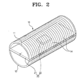
- FIG. 2 is a schematic perspective view of an image drum according to an exemplary embodiment of the present invention.
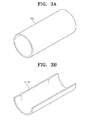
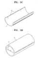
- FIGS. 3A through 3E are manufacturing process drawings of an image drum according to an exemplary embodiment of the present invention.
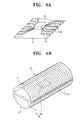
- FIGS. 4A and 4B are respectively a perspective view of a control unit according to an exemplary embodiment of the present invention and a perspective view of the control unit being connected to a drum body;
- FIGS. 5A and 5B are schematic exemplary drawings of an electrical connection method between the control unit and the drum body according to an exemplary embodiment of the present invention
- FIG. 6 is an exemplary alignment drawing of metal bumps formed on a conductive part of the control unit and electrodes of the drum body according to an exemplary embodiment of the present invention.
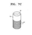
- FIGS. 7A through 7C are process drawings illustrating a method of forming line electrodes on the periphery of the drum body according to an exemplary embodiment of the present invention.
- FIG. 2 is a schematic perspective view of an image drum according to an exemplary embodiment of the present invention, wherein reference numeral 10 is a drum body, and 20 is a control unit.
- the drum body 10 is constructed in such a manner that a pair of symmetrical semi-cylindrical members 11 and 12 are coupled facing each other.
- the pair of semi-cylindrical members 11 and 12 are formed at a coupling surface thereof (identical meaning to 'cutting surface' to be described later) with a plurality of electrodes 13.
- control unit 20 includes a substrate 21 and a chip 22 (for example, an ASIC) packaged to the substrate 21.
- a chip 22 for example, an ASIC
- the conductive parts 23 and the non-conductive parts 24 may be simply formed by partially oxidizing the substrate 21.
- the drum body 10 and the control unit 20 are assembled in such a manner that both lateral portions of the substrate 21 formed with the conductive parts 23 and the non-conductive parts 24 are coupled by coupling surfaces of the semi-cylindrical members 11 and 12 while both lateral portions of the substrate 21 are inserted between the coupling surfaces of the semi-cylindrical members 11 and 12.
- the cut surfaces of the semi-cylindrical members 11 and 12 are formed with a plurality of electrodes 13 as illustrated in FIG. 3C.
- the photolithographic process is widely used in such areas as semiconductor process and the like, and there is little difference from the conventional process except that the cylindrical drum body 10 is rotated.
- the drum body 10 is rotated, and an injector 200 is used to coat photo resist on the surface of the drum body 10 as illustrated in FIG. 7A.
- exemplary embodiments of the present invention enable the complicated and accurate process as evidenced in the prior art to be dispensed with, and a reliable and excellent image drum can be manufactured using a simple process.
Landscapes
- Physics & Mathematics (AREA)
- General Physics & Mathematics (AREA)
- Printers Or Recording Devices Using Electromagnetic And Radiation Means (AREA)
- Electrophotography Using Other Than Carlson'S Method (AREA)
Applications Claiming Priority (1)
| Application Number | Priority Date | Filing Date | Title |
|---|---|---|---|
| KR1020050069220A KR100701295B1 (ko) | 2005-07-29 | 2005-07-29 | 화상 드럼 및 그 제작방법 |
Publications (2)
| Publication Number | Publication Date |
|---|---|
| EP1748324A1 true EP1748324A1 (de) | 2007-01-31 |
| EP1748324B1 EP1748324B1 (de) | 2008-08-13 |
Family
ID=37309722
Family Applications (1)
| Application Number | Title | Priority Date | Filing Date |
|---|---|---|---|
| EP06011691A Not-in-force EP1748324B1 (de) | 2005-07-29 | 2006-06-06 | Bildtrommel und ihr Herstellungsverfahren |
Country Status (5)
| Country | Link |
|---|---|
| US (1) | US20070024691A1 (de) |
| EP (1) | EP1748324B1 (de) |
| JP (1) | JP2007038648A (de) |
| KR (1) | KR100701295B1 (de) |
| DE (1) | DE602006002202D1 (de) |
Cited By (1)
| Publication number | Priority date | Publication date | Assignee | Title |
|---|---|---|---|---|
| EP1995637A1 (de) * | 2007-05-23 | 2008-11-26 | Samsung Electronics Co., Ltd. | Bilderzeugungselement und Herstellungsverfahren dafür und Bilderzeugungsvorrichtung |
Families Citing this family (4)
| Publication number | Priority date | Publication date | Assignee | Title |
|---|---|---|---|---|
| KR101436389B1 (ko) * | 2007-11-12 | 2014-09-02 | 삼성전자주식회사 | 이미지 드럼 제조방법 및 이미지 드럼 |
| JP5163191B2 (ja) * | 2008-03-11 | 2013-03-13 | 富士ゼロックス株式会社 | 画像形成装置 |
| JP5299085B2 (ja) * | 2009-05-27 | 2013-09-25 | 株式会社リコー | 潜像形成方法、潜像形成装置、画像形成装置および静電潜像計測装置 |
| US10636010B2 (en) * | 2017-10-26 | 2020-04-28 | Quotient Technology Inc. | System for bifurcated transaction for products at a brick-and-mortar store |
Citations (3)
| Publication number | Priority date | Publication date | Assignee | Title |
|---|---|---|---|---|
| EP0595388A1 (de) * | 1992-10-30 | 1994-05-04 | Océ-Nederland B.V. | Bilderzeugerherstellungsverfahren und ein Datenwiedergabedruckgerät |
| US6014157A (en) * | 1996-04-25 | 2000-01-11 | Oce-Technologies B.V. | Image forming element having accurate connection with the electronic components of the control unit |
| US6043830A (en) * | 1991-05-08 | 2000-03-28 | Cubital, Ltd. | Apparatus for pattern generation on a dielectric substrate |
Family Cites Families (4)
| Publication number | Priority date | Publication date | Assignee | Title |
|---|---|---|---|---|
| KR970062824A (ko) * | 1996-02-13 | 1997-09-12 | 김광호 | 화상형성장치에서 감광드럼의 표면전위 제어장치 |
| KR19980057456A (ko) * | 1996-12-30 | 1998-09-25 | 김광호 | 화상형성장치의 감광드럼 용지말림 방지방법 |
| KR100358343B1 (ko) * | 2000-05-16 | 2002-10-25 | 삼성전자 주식회사 | 화상형성장치의 감광드럼 오염방지 장치 |
| KR100403603B1 (ko) * | 2002-02-26 | 2003-10-30 | 삼성전자주식회사 | 화상형성장치용 감광드럼 구조체 |
-
2005
- 2005-07-29 KR KR1020050069220A patent/KR100701295B1/ko not_active Expired - Fee Related
-
2006
- 2006-04-05 US US11/397,703 patent/US20070024691A1/en not_active Abandoned
- 2006-06-06 EP EP06011691A patent/EP1748324B1/de not_active Not-in-force
- 2006-06-06 DE DE602006002202T patent/DE602006002202D1/de not_active Expired - Fee Related
- 2006-06-21 JP JP2006170900A patent/JP2007038648A/ja active Pending
Patent Citations (3)
| Publication number | Priority date | Publication date | Assignee | Title |
|---|---|---|---|---|
| US6043830A (en) * | 1991-05-08 | 2000-03-28 | Cubital, Ltd. | Apparatus for pattern generation on a dielectric substrate |
| EP0595388A1 (de) * | 1992-10-30 | 1994-05-04 | Océ-Nederland B.V. | Bilderzeugerherstellungsverfahren und ein Datenwiedergabedruckgerät |
| US6014157A (en) * | 1996-04-25 | 2000-01-11 | Oce-Technologies B.V. | Image forming element having accurate connection with the electronic components of the control unit |
Cited By (1)
| Publication number | Priority date | Publication date | Assignee | Title |
|---|---|---|---|---|
| EP1995637A1 (de) * | 2007-05-23 | 2008-11-26 | Samsung Electronics Co., Ltd. | Bilderzeugungselement und Herstellungsverfahren dafür und Bilderzeugungsvorrichtung |
Also Published As
| Publication number | Publication date |
|---|---|
| KR100701295B1 (ko) | 2007-03-29 |
| EP1748324B1 (de) | 2008-08-13 |
| US20070024691A1 (en) | 2007-02-01 |
| JP2007038648A (ja) | 2007-02-15 |
| KR20070014519A (ko) | 2007-02-01 |
| DE602006002202D1 (de) | 2008-09-25 |
Similar Documents
| Publication | Publication Date | Title |
|---|---|---|
| TWI320212B (en) | Method for manufacturing semiconductor device | |
| US7905008B2 (en) | Method of manufacturing a coil component | |
| TW492120B (en) | Semiconductor device and its manufacturing method, stacked type semiconductor device, circuit substrate and electronic machine | |
| JPS62188201A (ja) | 多層シ−トコイル | |
| TWI482255B (zh) | 藉由嵌入跡線界定之導電墊 | |
| EP1115086A2 (de) | Kontaktlose IC Karte und Verfahren zur ihrer Herstellung | |
| US7508073B2 (en) | Wiring board, semiconductor device using the same, and method for manufacturing wiring board | |
| EP1748324B1 (de) | Bildtrommel und ihr Herstellungsverfahren | |
| CN114446573B (zh) | 层叠线圈部件及层叠线圈部件的安装结构 | |
| JP4935828B2 (ja) | チップ素子およびその製造方法 | |
| US7999191B2 (en) | Method for making cable with a conductive bump array, and method for connecting the cable to a task object | |
| JPH11330843A (ja) | ヘリカルアンテナ | |
| JP2980402B2 (ja) | 回路部品搭載用中間基板の製造法 | |
| JP4209762B2 (ja) | 撮像装置 | |
| JP2004055666A (ja) | 平面コイル付き基板および多層コイルとそれらの製造方法そして揺動体 | |
| JP2894796B2 (ja) | 配線ガラス基板と回路基板との接続方法 | |
| US20230230757A1 (en) | Laminated coil component | |
| US6518672B2 (en) | Multi-layer wiring board substrate and semiconductor device using the multi-layer wiring substrate | |
| JPH0657478B2 (ja) | Icカ−ドの製造方法 | |
| JPH10189607A (ja) | 半田バンプ接続素子およびその製造方法 | |
| JP2533277Y2 (ja) | チップキャパシタの接地構造 | |
| JPH11288827A (ja) | 電子部品 | |
| KR20220118417A (ko) | 배선 회로 기판 | |
| JPH05238050A (ja) | 画像形成装置 | |
| JPS58138167A (ja) | 画像読み取り装置 |
Legal Events
| Date | Code | Title | Description |
|---|---|---|---|
| PUAI | Public reference made under article 153(3) epc to a published international application that has entered the european phase |
Free format text: ORIGINAL CODE: 0009012 |
|
| AK | Designated contracting states |
Kind code of ref document: A1 Designated state(s): AT BE BG CH CY CZ DE DK EE ES FI FR GB GR HU IE IS IT LI LT LU LV MC NL PL PT RO SE SI SK TR |
|
| AX | Request for extension of the european patent |
Extension state: AL BA HR MK YU |
|
| 17P | Request for examination filed |
Effective date: 20070314 |
|
| R17C | First examination report despatched (corrected) |
Effective date: 20070417 |
|
| AKX | Designation fees paid |
Designated state(s): DE FR GB |
|
| GRAP | Despatch of communication of intention to grant a patent |
Free format text: ORIGINAL CODE: EPIDOSNIGR1 |
|
| GRAS | Grant fee paid |
Free format text: ORIGINAL CODE: EPIDOSNIGR3 |
|
| GRAA | (expected) grant |
Free format text: ORIGINAL CODE: 0009210 |
|
| AK | Designated contracting states |
Kind code of ref document: B1 Designated state(s): DE FR GB |
|
| REG | Reference to a national code |
Ref country code: GB Ref legal event code: FG4D |
|
| REF | Corresponds to: |
Ref document number: 602006002202 Country of ref document: DE Date of ref document: 20080925 Kind code of ref document: P |
|
| PLBE | No opposition filed within time limit |
Free format text: ORIGINAL CODE: 0009261 |
|
| STAA | Information on the status of an ep patent application or granted ep patent |
Free format text: STATUS: NO OPPOSITION FILED WITHIN TIME LIMIT |
|
| 26N | No opposition filed |
Effective date: 20090514 |
|
| REG | Reference to a national code |
Ref country code: FR Ref legal event code: ST Effective date: 20100226 |
|
| PG25 | Lapsed in a contracting state [announced via postgrant information from national office to epo] |
Ref country code: FR Free format text: LAPSE BECAUSE OF NON-PAYMENT OF DUE FEES Effective date: 20090630 |
|
| PG25 | Lapsed in a contracting state [announced via postgrant information from national office to epo] |
Ref country code: DE Free format text: LAPSE BECAUSE OF NON-PAYMENT OF DUE FEES Effective date: 20100101 |
|
| GBPC | Gb: european patent ceased through non-payment of renewal fee |
Effective date: 20100606 |
|
| PG25 | Lapsed in a contracting state [announced via postgrant information from national office to epo] |
Ref country code: GB Free format text: LAPSE BECAUSE OF NON-PAYMENT OF DUE FEES Effective date: 20100606 |