EP1748332A2 - Funkempfangseinrichtung, und Funkuhr - Google Patents
Funkempfangseinrichtung, und Funkuhr Download PDFInfo
- Publication number
- EP1748332A2 EP1748332A2 EP20060014946 EP06014946A EP1748332A2 EP 1748332 A2 EP1748332 A2 EP 1748332A2 EP 20060014946 EP20060014946 EP 20060014946 EP 06014946 A EP06014946 A EP 06014946A EP 1748332 A2 EP1748332 A2 EP 1748332A2
- Authority
- EP
- European Patent Office
- Prior art keywords
- signal
- frequency
- circuit
- output
- conversion
- Prior art date
- Legal status (The legal status is an assumption and is not a legal conclusion. Google has not performed a legal analysis and makes no representation as to the accuracy of the status listed.)
- Granted
Links
Images










Classifications
-
- G—PHYSICS
- G04—HOROLOGY
- G04R—RADIO-CONTROLLED TIME-PIECES
- G04R20/00—Setting the time according to the time information carried or implied by the radio signal
- G04R20/08—Setting the time according to the time information carried or implied by the radio signal the radio signal being broadcast from a long-wave call sign, e.g. DCF77, JJY40, JJY60, MSF60 or WWVB
- G04R20/10—Tuning or receiving; Circuits therefor
-
- G—PHYSICS
- G04—HOROLOGY
- G04R—RADIO-CONTROLLED TIME-PIECES
- G04R20/00—Setting the time according to the time information carried or implied by the radio signal
- G04R20/08—Setting the time according to the time information carried or implied by the radio signal the radio signal being broadcast from a long-wave call sign, e.g. DCF77, JJY40, JJY60, MSF60 or WWVB
- G04R20/12—Decoding time data; Circuits therefor
Definitions
- the present invention relates to, for example, a radio wave receiving apparatus for receiving standard radio waves, a radio wave receiving circuit and a radio wave timepiece.
- time data that is, standard radio waves containing a time code are being transmitted.
- long wave standard radio waves of 40 kHz and 60 kHz with time codes which are amplitude modulated, using the standard time format are sent from two transmitting stations (Fukushima and Saga).
- This time codes are sent with the frame the cycle of which is 60 seconds, for every occasion when the place of minute of the exact time is updated, that is, for every 1 minute.
- the frequency-divided signal is not in perfect coincident with the frequency necessary for converting the frequency of a received signal into an intermediate frequency, thereby to make it impossible to perform an accurate detection due to a difference in frequency, which is also a problem.
- the input section 200 is constituted with switches and the like for executing various functions of the radio wave timepiece 1, to output a corresponding operational signal to the CPU 100 when these switches are operated.
- the display section 300 is constituted with a small-sized liquid crystal display and the like, to display the current time and the like on the basis of display signals input from the CPU 100.
- the clock circuit section 800 counts signals input from the oscillating circuit section 900 to measure the current time, to output the current time data to the CPU 100.
- the oscillating circuit section 900 is constituted with a crystal oscillator and the like, to output the reference frequency signal of 32.768 kHz.
- the mixer 6241 multiplies and synthesizes an input signal to the basic circuit 624 with a signal "g" input from the frequency divider circuit 625, thereby to output the result.
- the filter circuit 6242 is constituted with a LPF (low pass filter) and the like, to allow frequencies in a predetermined low range to pass through with respect to a signal input from the mixer 6241, however to cut off a frequency component outside the range.
- a pass band of the filter circuit 6242 is decided dependent on the frequency of an input signal and a signal "g" in the basic circuit 624.
- the filter circuit 6242 is constituted in such a way that a sum frequency of the input signal and the signal "g" is cut off while a difference frequency is allowed to pass through.
- the amplifier 6243 amplifies or attenuates a signal input from the filter circuit 6242 dependent on a control signal "i" input from the AGC circuit 627, to output the signal.
- the output of the amplifier 6243 is given as an output signal of the basic circuit 624.
- the frequency divider circuit 625 frequency-divides or frequency-multiplies a reference frequency signal bs input from the oscillating circuit section 900 by a plurality of ratios, to output the results as signals g1, g2, ... gn into the basic circuits 624[1], 624[2], ... 624[N], and also to output them as a signal "f" into a detection circuit 626.
- the detection circuit 626 detects a signal "a” input from the multi-stage frequency conversion circuit 623 by using the signal “f” input from the frequency divider circuit 625, and outputs it as a detected signal "d".
- the detected signal "d” is input into a time-code generating section 700 and is utilized to adjust the current time and the like.
- the AGC circuit 627 generates and outputs a control signal "h” to control an amplified degree of the RF amplifier circuit 622 and a control signal “i” to control an amplified degree of the amplifier 6243 in each of the basic circuits 624, depending on the strength of a signal "a" input from the multi-stage frequency conversion circuit 623.
- FIG. 4 is a view illustrating a circuit configuration of the detection circuit 626.
- the detection circuit 626 performs detection by referring to the signal "a" input from the multi-stage frequency conversion circuit 623.
- the detection circuit comprises a 1/2 frequency divider 6261, a logical gate 6262, mixers 6263 and 6264, LPFs 6265 and 6266, square circuits 6267 and 6268, and an adder 6269.
- the 1/2 frequency divider 6261 frequency-divides the signal "f" input from the frequency divider circuit 625 into 1/2 and outputs it as a signal e1.
- the frequency of the signal "f” which is input into the 1/2 frequency divider 6261 is set to be two times that of the signal "a”, and therefore the signal e1 which is output from the 1/2 frequency divider 6261 is equal to the frequency of the signal "a”.
- the logical gate 6262 performs an exclusive OR (EOR) operation of the signal "f" with the signal e1 input from the 1/2 frequency divider 6261, to output the calculation result as a signal e2. Therefore, the signal e2 is a signal obtained by shifting the phase of the output signal e1 by 90 degrees (phase shift).
- the mixer 6263 multiplies and synthesizes a signal "a" input from the multi-stage frequency conversion circuit 623 with a signal e1 input from the 1/2 frequency divider 6261, thereby to output the result.
- the LPF 6265 allows frequencies in a predetermined low range to pass through, with respect to a signal input from the mixer 6263, however to cut off a frequency component outside the range, and outputs a signal "b".
- the square circuit 6267 squares the signal "b" input from the LPF 6265 and outputs the result.
- the mixer 6264 multiplies and synthesizes a signal "a" input from the multi-stage frequency conversion circuit 623 with a signal e2 input from the logical gate 6262 and outputs the result.
- the LPF 6266 allows frequencies in a predetermined low range to pass through, with respect to a signal input from the mixer 6264, however, cuts off a frequency component outside the range, thereby to output it as a signal "c".
- the square circuit 6268 squares the signal "c” input from the LPF 6266 and outputs the result.
- the adder 6269 adds a signal input from the square circuit 6267 to a signal input from the square circuit 6268, to output the result as a detected signal d.
- a conversion signal whose frequency is decreased by the multi-stage frequency conversion circuit 623, a signal "f" input from the frequency divider circuit 625 and a signal obtained by performing a 90-degree phase shift to the signal "f" are multiplied and squared, and both signals are added to perform detection. Namely, a sum of squares of I and Q components of the conversion signal is calculated, thereby it enables to perform accurate detection even when a slight difference in frequency or phase between the conversion signal and a reference signal causes.
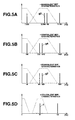
- a signal of 7232 Hz output from the basic circuit 624[1] being the previous stage and a signal g2 of 8192 Hz output from the frequency divider circuit 625, obtained by frequency-dividing by 4 the signal of 32768 Hz which is a reference frequency signal bs are input.
- the input signal of 7232 Hz and the signal g2 of 8192 Hz are multiplied and synthesized to generate a signal of 15424 Hz and a signal of 960 Hz, which are a sum of and a difference between these two frequencies, respectively.
- the basic circuit 624[2] is equivalent to a BPF which includes 3272Hz of the input signal in a pass band. Further, the pass band of the equivalent BPF is dependent on the pass band of the filter circuit 6242. However, since the pass band of the filter circuit 6242 in the basic circuit 624[2] is narrower than that of the filter circuit 6242 in the basic circuit 624[1], the pass band of the equivalent BPF in the basic circuit 624[2] is narrower than that of the equivalent BPF in the basic circuit 624[1].
- a signal of 960 Hz output from the basic circuit 624[2] being the previous stage and a signal g7 of 1024 Hz output from the frequency divider circuit 625, obtained by frequency-dividing by 32 the signal of 32768 Hz which is a reference frequency signal bs are input.
- the input signal of 960 Hz and the signal g7 of 1024 Hz are multiplied and synthesized to generate a signal of 1984 Hz and a signal of 64 Hz, which are a sum of and a difference between these two frequencies, respectively.
- the basic circuit 624[3] is equivalent to a BPF which includes 1024Hz of the input signal in a pass band. Further, the pass band of the equivalent BPF is dependent on the pass band of the filter circuit 6242. However, since the pass band of the filter circuit 6242 in the basic circuit 624[3] is narrower than that of the filter circuit 6242 in the basic circuit 624[2], the pass band of the equivalent BPF in the basic circuit 624[3] is narrower than that of the equivalent BPF in the basic circuit 624[2].
- the detection circuit 626 is equivalent to a BPF which includes 64Hz in a pass band. Further, the pass band of the equivalent BPF is dependent on the pass band of the filter circuit 6242. However, since the pass band of the LPFs 6265 and 6266 is narrower than that of the filter circuit 6242 in the basic circuit 624[3], the pass band of each LPF is narrower than that of the equivalent BPF in the basic circuit 624[3].
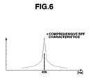
- the radio wave receiving apparatus 620 is, as a whole, equivalent to four stages of BPF connected in series. As illustrated in FIG. 6, it can be regarded as a BPF having an extremely narrow band centered on 40 kHz, which is a reception frequency.
- FIG. 6 is a view on an assumption that an operation of receiving standard radio waves given in FIG. 5A to FIG. 5D is regarded as a BPF having an extremely narrow band or as a comprehensive BPF.
- an input signal output from the basic circuit 624 of the stage just before each of the basic circuits 624 is multiplied and synthesized with signals "g" (g2, g4 and g7) to decrease the frequency, so that the frequency of the received signal input from the RF amplifier circuit 622 is gradually decreased. That is, since the pass bands of the equivalent BPF of the basic circuits 624 are gradually narrower, the radio wave receiving apparatus 620 in its entirety can be regarded as a BPF having an extremely narrow band centered on the frequency of the received signal.
- the signal "a" input into the detection circuit 626 is actually not in perfect coincident with the signal “f” in frequency and phase, and thereby results in a possible deformation of the waveform of a detected signal "d".
- the sum of squares of I and Q components of the signal "a” is calculated at the detection circuit 626, thereby to make it possible to prevent the deformation of a waveform of the detected signal "d” resulting from the deviation and to perform accurate detection.
- signals b and c are squared by the square circuits 6267 and 6268, respectively, and added by an adder 6269 to output a detection signal "d" from the detection circuit 626.
- the multi-stage frequency conversion circuit 623 is constituted with five stages of basic circuits, namely, 624[1], 624[2]... 624[5].
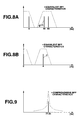
- FIG. 7A to FIG. 7D, FIG. 8A to FIG. 8B and FIG. 9 are views illustrating images of frequency spectrum for explaining a signal-receiving operation in this case.
- a received signal of 77.5 kHz from the RF amplifier circuit 622 and a signal g1 of 65.536 kHz obtained by multiplying by 2 a signal of 32.768 kHz which is a reference frequency signal bs output from the frequency divider circuit 625 are input into the first stage of the basic circuit 624[1].
- the mixer 6241 multiplies and synthesizes the received signal of 77.5 kHz with the signal g1 of 65.536 kHz, to output a signal of 11.964 kHz which is the difference between these two frequencies, as an output signal of the basic circuit 624[1], after passing through the filter circuit 6242.
- the basic circuit 624[1] can be regarded to be equivalent to a BPF which includes 77.5 kHz of the input signal in a pass band.
- a signal of 11964 Hz output from the basic circuit 624[1] being the previous stage and a signal g4 of 8192 Hz output from the frequency divider circuit 625, obtained by frequency-dividing by 4 the signal of 32768 Hz which is a reference frequency signal bs are input.
- the input signal of 11964 Hz and the signal g4 of 8192 Hz are multiplied and synthesized and a signal of 3772 Hz which are a difference between these two frequencies passes through the filter circuit 6242 to output as the output signal of the basic circuit 624[2].
- the basic circuit 624[2] can be regarded to be equivalent to a BPF which includes 8192Hz of the input signal in a pass band.
- the pass band of the equivalent BPF is narrower than that of the equivalent BPF in the basic circuit 624[1].
- a signal of 3772 Hz output from the basic circuit 624[2] being the previous stage and a signal g5 of 8192 Hz output from the frequency divider circuit 625, obtained by frequency-dividing by 8 the signal of 32768 Hz which is a reference frequency signal bs are input.
- the input signal of 3372 Hz and the signal g4 of 4096 Hz are multiplied and synthesized to generate a signal of 324 Hz which is the difference between these two frequencies.
- the signal of 324 Hz passes through the filter circuit 6242 and outputs as the output signal of the basic circuit 624[3].
- a signal of 324 Hz output from the basic circuit 624[3] being the previous stage and a signal "g9" of 256 Hz output from the frequency divider circuit 625, obtained by frequency-dividing by 128 the signal of 32768 Hz which is a reference frequency signal are input.
- the signal of 324 Hz and the signal g4 of 256 Hz are multiplied and synthesized to generate a signal of 68 Hz which is the difference between these two frequencies.
- the signal of 68 Hz passes through the filter circuit 6242 and outputs as the output signal of the basic circuit 624[4].
- the basic circuit 624[4] can be regarded to be equivalent to a BPF which includes 324Hz of the input signal in a pass band.
- the pass band of the equivalent BPF is narrower than that of the equivalent BPF in the basic circuit 624[3].
- a signal of 68 Hz output from the basic circuit 624[4] being the previous stage and a signal g11 of 64 Hz output from the frequency divider circuit 625, obtained by frequency-dividing by 512 the signal of 32768 Hz which is a reference frequency signal are input.
- the signal of 68 Hz and the signal g11 of 64 Hz are multiplied and synthesized to generate a signal of 4 Hz which is the difference between these two frequencies.
- the signal of 4 Hz passes through the filter circuit 6242 and outputs as the output signal of the basic circuit 624[5].
- This output signal is also the output signal of the multi-stage frequency conversion circuit 623.
- the basic circuit 624[5] can be regarded to be equivalent to a BPF which includes 68Hz of the input signal in a pass band.
- the pass band of the equivalent BPF is narrower than that of the equivalent BPF in the basic circuit 624[3].
- the detection circuit 626 the signal "a" of 4 Hz output from the multi-stage frequency conversion circuit 623 and the signal g15 as a signal "f", of 4 Hz output from the frequency divider circuit 625, obtained by frequency-dividing by 8182 the signal of 32768 Hz which is the reference frequency signal bs, are input and detected. That is, as illustrated in FIG. 8B, the input signal “a” of 4 Hz and the signal “f” of 4 Hz are multiplied and synthesized to generate a signal of 0 Hz which a difference between these two frequencies. The generated signal is output as a detection signal "d" output from the detection circuit 626.
- the detection circuit 626 can be regarded to be equivalent to a BPF which includes 4Hz of the input signal in a pass band.
- the pass band of the equivalent BPF is narrower than that of the equivalent BPF in the basic circuit 624[5].
- the multi-stage frequency conversion circuit 623 may be constituted with four stages of basic circuits 624[1],624[2], ... and 624[4].
- a signal "a” of 68 Hz from the multi-stage frequency conversion circuit 623 and a signal “f” of 64 Hz from the frequency divider circuit 625 are respectively input into the detection circuit 626 to perform detection.
- a detected signal "d” of 4 Hz which is a difference between these two frequencies, is output, since the detection circuit 626 is used to detect only amplitude components of signals, there are no problem for detection, namely, for reproduction of received signals.
- FIG. 10 is a table showing frequencies of signals "g" input from the frequency divider circuit 625 into each of the basic circuits 624 in the multi-stage frequency conversion circuit 623 and frequencies of output signals of the basic circuit 624 when receiving standard radio waves different in frequency in various countries. This figure shows the following cases, 1) Japan (40 kHz), 2) Japan (60 kHz), 3) Germany (77.5 kHz), 4) Switzerland (70 kHz) and 5) China (68.5 kHz).
- the signal of 2656 Hz and a signal "g6" of 2048 Hz are multiplied and synthesized, and converted into a signal of 608 Hz.
- the signal of 608 Hz and a signal "g8” of 512 Hz are multiplied and synthesized, and converted into a signal of 96 Hz
- the signal of 96 Hz and a signal "g10" of 128 Hz are multiplied and synthesized, and converted into a signal of 32 Hz.
- the signal of 32 Hz and a signal "g12" of 32 Hz as a signal "f” are input into the detection circuit 626 to perform detection.
- n-stages of basic circuits 624 connected in series in the multi-stage frequency conversion circuit 623 convert standard radio waves received from the receiving antenna 621 into lower frequencies sequentially on the basis of signals "g" input from the frequency divider circuit 625. Then, signals output from the multi-stage frequency conversion circuit 623 are detected by the detection circuit 626.
- Embodiment 1 will be explained as follows.
- a multi-stage frequency conversion circuit 623 is constituted with a plurality of basic circuits 624 connected in series.
- Each of the basic circuits 624 is different from one another in pass band set in a filter circuit 6242, depending on a frequency of a standard radio wave to be received and a stage at which the basic circuit 624 is arranged in the multi-stage frequency conversion circuit 623. Therefore, in Embodiment 1, the individual basic circuits 624 are constituted as follows.
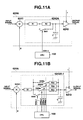
- FIG. 11A is a view illustrating a circuit configuration of the basic circuit 624A in Embodiment 1.
- the basic circuit 624A includes a mixer 6241, a filter circuit 6242A and an amplifier 6243.
- the filter circuit 6242A is provided with registers R1 and R2 connected in series, a capacitor C and a switch SW1 connected to the register R2 in parallel.
- the switch SW1 is operated by an input from a CPU 100, for example.
- ON/OFF connection/disconnection
- SW1-1 for instructing to switch a pass band of the filter circuit 6242A.
- the switch SW1 when the switch SW1 is ON, a signal input from the mixer 6241 to the filter circuit 6242A passes through the register R1 and the switch SW1 to output, while the filter circuit 6242A functions as an RC filter having the register R1 and the capacitor C.
- the switch SW1 when the switch SW1 is OFF, a signal input into the filter circuit 6242A passes through the registers R1 and R2, and is output, while the filter circuit 6242A functions as an RC filter having the registers R1, R2 and the capacitor C. More specifically, the switch SW1 is turned ON/OFF by a bandwidth switching signal to be input, and thereby a time constant of the filter circuit 6242A is changed, or a pass band is switched.
- the filter circuit 6242A may be set for a pass band so as to cut off a sum frequency of an input signal to the basic circuit 624 and a signal "g" and also allow a difference frequency to pass through. Therefore, it is possible to realize a radio wave receiving apparatus 620 which enables conversion to a larger scale integration easily and general use, by providing the multi-stage frequency conversion circuit 623 which has a plurality of basic circuits 624A with the same constitution, connected in series, and in which for example, a bandwidth switching signal input from the CPU 100 is used for setting a pass band of each of the basic circuits 624.
- switches SW6, SW6a, SW6b, SW6c, ... are controlled for ON/OFF by switching control signals (SW6-1, SW6a-2, SW6b-3, SW6c-4, ...) input from the CPU 100, for example. Thereby, it is possible to set a pass band of the filter circuit 6242A-1 so as to be switched to 3 or more stages.
- Embodiment 2 will be explained as follows.
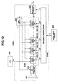
- the multi-stage frequency conversion circuit 623B is constituted with N-stages of a plurality of basic circuits 624[1], 624[2], ... 624[N]. Then, signals g1, g2, ... "gN" from the frequency divider circuit 625B are input into the basic circuits 624[1], 624[2], ..., 624[N], respectively, and for example, a use/non-use switching signal sf is input from the CPU 100.
- signals g1, g2, ..., "g16” having 65768, 32768, 16384, 8192, ..., 4 and 2 Hz, obtained by frequency-dividing the signal of 32768 Hz by the respective frequency dividing ratios of 2, 1, 1/2, 1/4, ..., 1/8182 and 1/16384, respectively, is output from a frequency divider circuit 625.
- These signals g1, g2, ..., "g16” are input into basic circuits 624[1], 624[2], ..., 624[16], respectively.
- the use/non-use switching signal sf means a signal for specifying the use/non-use of individual basic circuits 624[1], 624[2], ..., 624[N].
- "To use” the basic circuits 624[1], 624[2], ..., 624[N] means that in the basic circuit 624 concerned, synthesis is made by multiplying a signal "g" input from the frequency divider circuit 624 by an input signal from the previous stage to decrease the frequency, namely, to perform frequency conversion, while “not to use” the basic circuits (non-use) means that an input signal is output with no frequency conversion performed in the input signal.
- individual basic circuits 624 [1], 624 [2], ..., 624 [N] which constitute the multi-stage frequency conversion circuit 623B are used or not is dependent on the frequency of a standard radio wave to be received.
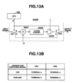
- FIG. 13A is a view illustrating a basic circuit 624B, which is one circuit configuration, among basic circuits 624[1], 624[2], ..., 624[N] constituting the multi-stage frequency conversion circuit 623B in Embodiment 2.
- the basic circuit 624B is constituted with switches SW2, SW3, a mixer 6241, a filter circuit 6242 and an amplifier 6243.
- the switch SW2 is provided at the previous stage of the mixer 6241 and connected to either of terminals a or b, depending on a use/non-use switching control signal sf input from a CPU 100.
- the switch SW3 is provided at the subsequent stage of the amplifier 6243, and connected to either of the terminals "a” or "b", depending on the use/non-use switching control signal sf to be input.
- FIG. 13B is a table illustrating the relationship between the use/non-use switching signal sf and the connection state of switches SW2 and SW3.
- the switching signal specifies the use
- the switch SW2 is connected to the terminal "a"
- the switch SW3 is connected to the terminal "a”. Therefore, the input signal is multiplied and synthesized with a signal "g" input from the frequency divider circuit 625 by the mixer 6241 and is frequency-converted.
- the frequency-converted signal passes through the filter circuit 6242 and the amplifier 6243 to output as an output signal of the basic circuit 624B. Namely, the basic circuit 624 is in a state of "use.”
- the switch SW2 When the use/non-use switching signal sf specifies "non-use", the switch SW2 is connected to the terminal "b", while the switch SW3 is connected to the terminal "b". Therefore, the input signal is not subjected to frequency conversion but output as an output signal of the basic circuit 624, without any change. Namely, the basic circuit 624 is in a "non-use" state.
- the multi-stage frequency conversion circuit 623B is constituted with a plurality of basic circuits 624B identical in constitution, and a use/non-use switching signal sf input externally is used to switch the use/non-use of individual basic circuits 624B. Therefore, the use/non-use switching signal sf is set in accordance with a frequency of a standard radio wave to be input, thereby to make it possible to provide a general-purpose radio wave receiving apparatus 620 in which only the necessary basic circuit 624B is used but other basic circuits 624 are not used.
- Embodiment 3 is an embodiment of a multiband radio wave receiving apparatus 620, and different from Embodiment 2 in that the basic circuit 624B shown in FIG. 13A is replaced by the basic circuit 624C shown in FIG. 14A.
- FIG. 14A is a view illustrating a circuit configuration of a basic circuit 624C in Embodiment 3.
- the basic circuit 624C is constituted with a mixer 6241, a filter circuit 6242C, an amplifier 6243 and a switch SW4.
- the switch SW4 is provided between the mixer 6241 and the frequency divider circuit 625, and controlled for ON/OFF in accordance with a use/ non-use switching control signal sf input from the CPU 100.
- the filter circuit 6242C is provided with serially-connected registers R1 and R2, a capacitor C and a switch SW5 connected in parallel to the register R2.
- the switch SW5 is controlled for ON/OFF in accordance with a use/ non-use switching signal input from the SW5.
- FIG. 14B is a view illustrating the relationship between the use/non-use switching signal sf and the connection state of the switch SW5.
- the switch SW4 when "use" is specified by the use/non-use switching signal sf, the switch SW4 is turned on, while the switch SW5 is turned off. Therefore, the mixer 6241 performs synthesis by multiplying the input signal by a signal "g" input from the frequency divider circuit 625 to perform frequency conversion, and outputs as an output signal of the basic circuit 624C.
- the filter circuit 6242C functions as a low pass filter having a pass band dependent on the respective register values of the registers R1, R2 and a capacitance value of the capacitor C. Namely, the basic circuit 624 is in a "use" state.
- the switch SW4 is turned off and the switch SW5 is turned on. Therefore, since a signal "g" from the frequency divider circuit 625 is not input into the mixer 6241, an input signal is not subjected to frequency conversion but passes through the filter circuit 6242C and outputs as an output signal. Namely, the basic circuit 624 is in a state of "non-use.”
- the filter circuit 6242C is given as a RC filter made up of the register R1 and the capacitor C, but the register R1 is so small in register value that it will not actually function as a filter.
- the multi-stage frequency conversion circuit 623 is constituted with a plurality of basic circuits 624C identical in constitution, and a use/non-use switching signal input from the outside is used to switch the use/non-use of individual basic circuits 624C. Therefore, the use/non-use switching signal sf is set in accordance with a frequency of a standard radio wave to be received, thereby to make it possible to provide a general-purpose radio wave receiving apparatus 620, in which only the necessary basic circuits 624C are used but other basic circuits 624C are not used.
- FIG. 15 is a block diagram illustrating a schematic constitution of a radio wave receiving apparatus 620D in Embodiment 4.
- the radio wave receiving apparatus 620D is constituted with a receiving antenna 621, an RF amplifier circuit 622, a multi-stage frequency conversion circuit 623, a frequency divider circuit 625D, a detection circuit 626, an AGC circuit 627 and a switch group 628.
- the frequency divider circuit 625D is provided with a plurality of output terminals of t1, t2, t3, ..., tm for outputting signals g1, g2, g3, ..., gm obtained by frequency-dividing a reference frequency signal bs input from the transmitting circuit section 900 by the frequency dividing ratios of 2, 1, 1/2, 1/4, ..., 1/2( m-2 ) (m is an integral number), respectively.
- a frequency of a signal "g" input into each of the basic circuits 624 in the multi-stage frequency conversion circuit 623 is different, depending on the frequency of a standard radio wave to be received.
- a selected signal "st" input from outside is used to switch the connection of each of the switches S in the switch group 628 provided between each of the basic circuits 624 and the detection circuit 626, and the frequency divider circuit 625, thereby to make it possible to switch a frequency of a signal "g" input into the basic circuits 624[1], 624[2], ..., 624[N] and to provide a multiband radio wave receiving apparatus 620 with a general-purpose composition.
- an input signal is frequency-converted (down conversion) on the basis of a frequency-divided signal "g".
- g frequency-divided signal
- a signal of frequency ⁇ when a signal of frequency ⁇ is received, frequency conversion performed by using a frequency-divided signal of frequency ⁇ 1 as a local signal will result in a fact that a signal of frequency (image signal 1) positioned symmetrically to a desired signal to be received with respect to the frequency ⁇ 1, on a frequency axis, in addition to a signal of the desired frequency ⁇ to be received (the desired signal), as illustrated in FIG. 17A.
- a frequency conversion is performed for each of the desired signal to be received and the image signal 1. Namely, by the frequency conversion for the desired signal to be received, a signal of frequency (image signal 2) positioned symmetrically to the desired signal to be received, with respect to the frequency ⁇ 2 is also received. Further, by the frequency conversion for the image signal 1, a signal of frequency (image signal 3) positioned symmetrically to the image signal 1, with respect to the frequency ⁇ 2 i is received. The frequency ⁇ 2 i is a frequency positioned symmetrically to the frequency of ⁇ 2 with respect to the frequency ⁇ 1.
- the phase shifter 6244 performs a 90-degree phase shift to a signal "g" input from the frequency divider circuit 625, thereby to output it as a signal "g i ".
- the mixer 6245a makes synthesis by multiplying an input signal into the basic circuit 624F by a signal “g”, thereby to output them as a signal “f 1I ".
- the mixer 6245b makes synthesis by multiplying an input signal by a signal "g i " input from the phase shifter 6244, thereby to output them as a signal "f 1Q ".
- FIG. 19 is a view illustrating the circuit configurations of the phase-shift circuit 6246a and 6246b.
- the phase-shift circuits 6246a and 6246b are identical in constitution and constituted with a two-stage APF (All Pass Filter) 6247 connected in series.
- the APF 6247 is a filter which allows only a phase to change and is provided with an operational amplifier OP, registers R1, R2, and R3 and a capacitor C1.
- An output level of the APF 6247 is dependent on values of the registers R1 and R2, and a phase shift level of the APF 6247 is dependent on those of the register R3 and the capacitor C1. Since a one-stage APF 6247 can perform a phase shift up to 180 degrees, the phase-shift circuits 6246a and 6246b comprising a two-stage APF 6247 can perform a phase shift up to 360 degrees.
- the adder-subtractor 6247 makes synthesis by adding or subtracting a signal "f 2I " input from the phase-shift circuit 6246a to or from a signal “f 2Q “ input from the phase-shift circuit 6246b, thereby to output them as a signal "f 3 ", for example, depending on a sum/difference switching signal wsk input from a CPU 100.
- the filter circuit 6248 is an LPF (Low Pass Filter), allowing frequencies in a predetermined low range to pass through with respect to a signal "f 3 " input from the adder-subtractor 6247, while cutting off frequency components beyond the range.
- the filter circuit 6248 includes serially-connected registers R4 and R5, a capacitor C2 and a switch SW1 connected in parallel to the register R4.
- the switch SW1 is controlled for ON/OFF, for example, depending on a time constant switching signal tk input from the CPU 100.
- the switch SW1 is switched ON/OFF, thereby to change a time constant of the filter circuit 6248, namely, to switch a pass band.
- An output signal from the filter circuit 6248 is given as an output signal of a basic circuit 624F.
- the basic circuit 624F generates input signals of I and Q signals, allows the generated Q signal to undergo a 90-degreephase shift with respect to the I signal to effect synthesis, thereby removing an image signal.
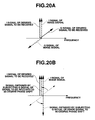
- FIG. 20A and FIG. 20B are views for explaining a principle of removing an image signal by the basic circuit 624F, a lengthwise direction is given as a real axis (I component), and an oblique depth direction is given as an imaginary axis (Q component) to indicate a concept of the phase-shift relationship between a desired signal to be received and an image signal. Further, the solid line indicates the desired signal to be received and the dotted line indicates the image signal.
- a desired signal to be received and an image signal respectively have I and Q signals, which are mutually orthogonal. Since the desired signal to be received is positioned symmetrical with respect to the image signal mainly at a frequency of a frequency-divided signal "g" (local signal) on a frequency axis, the respective I signals of the desired signal to be received and the image signal are in phase, while the respective Q signals of the desired signal to be received and the image signal are in reverse phase.
- g local signal
- the mixers 6245a and 6245b use signals (signals “g” and “g i ”) in which input signals are mutually orthogonal to effect frequency conversion, thereby to generate I and Q signals (signal “f 1I “ and “f 1Q "). Then, the generated I and Q signals are phase-shifted by the phase-shift circuits 6246a and 6246b (signals “f 2I “ and “f 2Q "), and added/subtracted by the adder-subtractor 6247, thereby removing an image signal and outputting only a desired signal to be received.
- each of the basic circuits 624F is constituted in such a way that each signal obtained by subjecting the respective input signals of I and Q signals to frequency conversion by using a signal "g" is phase-shifted to give a 90-degree phase-shift difference, added and synthesized, thereby to make it possible to remove an image signal component resulting from the frequency conversion.
- the serially-connected basic circuit 624F multiplies an input signal by a signal "g" input from the frequency divider circuit 625 and a signal obtained by subjecting the signal "g” to a 90-degree phase shift, allows the multiplied signals to undergo a phase shift so as to give a 90-degree phase-shift difference with respect to each of the multiplied signals, and adds and subtracts them to output as a conversion signal.
- I and Q signals obtained by subjecting the input signal to frequency conversion are phase-shifted so as to respectively give a 90-degree phase-shift difference, added and subtracted, thereby to make it possible to remove an image signal component resulting from the frequency conversion.
- each of serially connected basic circuits 624 in a multi-stage frequency conversion circuit 623 makes synthesis by multiplying received signals received at a receiving antenna 621 by a signal "g" obtained by dividing a reference frequency signal bs at a predetermined frequency dividing ratio, thereby gradually decreasing the frequency. Then, in a detection circuit 626, detection is performed on the basis of a signal "a", the frequency of which is decreased, thereby to output a detected signal "d".
- each of the basic circuits 624 may be constituted with simple circuit elements, thereby to make it possible to provide a large-scale integration and reduce the dimension of chips, although the circuits are provided in a multiple stage and accordingly made larger in size.
- an embodiment in which the present invention is applicable is not limited to the embodiments described above but may be changed appropriately within a scope not deviating from an object of the present invention.
- the detection circuit 626 performs detection on the basis of a signal "a" output from the multi-stage frequency conversion circuit 623 to output a detected signal "d".
- a final stage of the basic circuit 624 in the multi-stage frequency conversion circuit 623 may also act as the detection circuit 626.
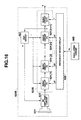
- FIG. 16 is a block diagram illustrating a constitution of a radio wave receiving apparatus 623E in this case.
- the radio wave receiving apparatus 623E is different in constitution from the radio wave receiving apparatus 623 shown in FIG. 2 in that it is provided with the multi-stage frequency conversion circuit 623E including serially connected n-stages of basic circuits 624[1], 624[2], ..., 624[N] and 624[n+1] but not provided with the detection circuit 626.
- a signal “a” from the previous stage of the basic circuit 624[N] and a signal “f” obtained by dividing a reference frequency signal bs from the frequency divider circuit 625 by a predetermined frequency dividing ratio, which is identical in frequency with the signal "a", are respectively input into the final stage of the basic circuit 624[n+1] in the multi-stage frequency conversion circuit 623. Then, the basic circuit 624[n+1] outputs the signal “a” and a signal d, which is a difference frequency signal of the signal "f". Since the signal "a” and the signal “f” are identical in frequency, the signal “d” is of 0 Hz. In other words, the output signal "d" from the multi-stage frequency conversion circuit 623 is a detected signal which has detected the signal "a”, namely, a signal which has regenerated a received signal.
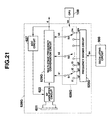
- the radio wave receiving apparatus 620 may be constituted as illustrated in FIG. 21, which is a constitution in which the detection circuit 626 is included in the multi-stage frequency conversion circuit 623.
- FIG. 21 is a block diagram illustrating a constitution of a radio wave receiving apparatus 620G in this case.
- the radio wave receiving apparatus 620G is to remove an image signal according to the same principle of Embodiment 5 described above, and constituted with a receiving antenna 621, a RF amplifier circuit 622, a multi-stage frequency conversion circuit 626G, a frequency divider circuit 625G, an AGC circuit 627 and a switch group 628G. Additionally, an explanation will be omitted for a block of functions and constitutions which is similar to that explained in FIG. 2.
- the frequency divider circuit 625G divides a reference frequency signal bs input from a transmitting circuit section 900 by the respective frequency dividing ratios of 2, 1, 1/2, 1/4, ..., 1/2 (m-2) (m is an integral number) and outputs the divided signals g1, g2, g3, ..., gm respectively at output terminals of t1, t2, t3, ..., tm.
- the switch group 628G includes a plurality of switches S1 to S3 provided between a multi-stage frequency conversion circuit 629G and a frequency divider circuit 625G. These switches S1 to S3 are respectively connected to any one of output terminals t1, t2, ..., tm of the frequency divider circuit 625G, for example, in accordance with a selected signal ss input from a CPU 100. Then, signals "g" output to the output terminals t connected to the respective switches S1 to S3 are input into the multi-stage frequency conversion circuit 629G as signals k1 to k3.
- the multi-stage frequency conversion circuit 629G converts input signals from the RF amplifier circuit 622 into those having gradually lower frequencies on the basis of signals k1 to k3 input via the switch group 628G from the frequency divider circuit 625G and outputs them as signals "d".
- the mixer 6292a makes synthesis by multiplying a signal input into the multi-stage frequency conversion circuit 629G by a signal k1 to output them as a signal f a1I .
- the filter 6293a is an LPF, allowing frequencies in a low frequency range including a difference frequency between the input signal and the signal k1 to pass through with respect to the signal f a1I input from the mixer 6292a to output them, while cutting off frequency components beyond the range including a sum frequency.
- the phase shifter 6291a allows the input signal k1 to undergo a 90-degree phase shift and outputs it as a signal k4.
- the mixer 6292b makes synthesis by multiplying the input signal by the signal k4 input from the phase shifter 6291a, thereby to output them as a signal f a1Q .
- the filter 6293b is a LPF, allowing frequencies in a low frequency range including a difference frequency between the input signal and the signal k1 to pass through with respect to the signal f a1Q input from the mixer 6292b to output them, while cutting off frequency components beyond the range including a sum frequency.
- the mixer 6292e makes synthesis by multiplying the signal f a1Q input via the filter 6293b from the mixer 6292b by the signal k2 to output them as a signal "f b2I ".
- the filter 6293e is a LPF, allowing frequencies in a low frequency range including a difference frequency between the signal "f a1Q " and the signal k2 to pass through with respect to the signal f b2I input from the mixer 6292e to output them, while cutting off frequency components beyond the range including a sum frequency.
- the mixer 6292f makes synthesis by multiplying the signal f a1Q input via the filter 6293b from the mixer 6292b by the signal k5 input from the phase shifter 6291b to output them as a signal f b2Q .
- the filter 6293f is a LPF, allowing frequencies in a low frequency range including a difference frequency between the signal f a1Q and the signal k2 to pass through with respect to the signal f b2Q input from the mixer 6292f to output them, while cutting off frequency components beyond the range including a sum frequency.
- the adder-subtractor 6294a makes synthesis by adding or subtracting a signal f b1I input via the filter 6293c from the mixer 6292c to and from a signal f b2Q input via the filter 6293f from the mixer 6292f, thereby to output them in accordance with a sum/difference switching signal 1 (wsk 1) to be input.
- the sum/difference switching signal 1 (wsk 1) is a signal for specifying operational contents (addition/subtraction) of the adder-subtractor 6294a and input, for example, from a CPU 100.
- the adder-subtractor 6294b makes synthesis by adding or subtracting a signal f b1Q input via the filter 6293d from the mixer 6292d to and from a signal f b2I input via the filter 6293e from the mixer 6292e in accordance with a sum/difference switching signal 2 (wsk 2) to be input, thereby to output them.
- the sum/difference switching signal 2 (wsk 2) is a signal for specifying operational contents of the adder-subtractor 6294b and input, for example, from a CPU 100.
- the adder-subtractor 6294b makes synthesis by adding the signal f b1Q to the signal f b2I thereby to output them as a signal fg, where "addition" is specified by the sum/difference switching signal 2 (wsk 2), and makes synthesis by subtracting the signal f b1Q from the signal f b2I , thereby to output them as a signal f e , where "subtraction" is specified.
- the mixer 6292g makes synthesis by multiplying a signal input from the adder-subtractor 6294a by a signal k3 to output them. More specifically, where a signal f c is input from the adder-subtractor 6294a, it makes synthesis by multiplying the signal f c by the signal k3 to output them as a signal f cI3 , and where a signal f d is input, it makes synthesis by multiplying the signal f d by the signal k3 to output them as a signal f dI3 .
- the phase shifter 6291c allows the input signal k3 to undergo a 90-degree phase shift and outputs it as a signal k6.
- the mixer 6292h makes synthesis by multiplying a signal input from the adder-subtractor 6294b by the signal k6 input from the phase shifter 6291c to output them. More specifically, where a signal f e is input from the adder-subtractor 6294b, it makes synthesis by multiplying the signal f e by the signal k6 to output them as a signal f eQ3 , and where a signal f g is input, it makes synthesis by multiplying the signal f g by the signal k6 to output them as a signal f gQ3 .
- the mixer 6292i makes synthesis by multiplying a signal input from the adder-subtractor 6294b by a signal k3 to output them. More specifically, where a signal f e is input from the adder-subtractor 6294b, it makes synthesis by multiplying the signal f e by the signal k3 to output them as a signal f eI3 , and where a signal f g is input, it makes synthesis by multiplying the signal f g by the signal k3 to output them as a signal f gI3 .
- the mixer 6292j makes synthesis by multiplying a signal input from the adder-subtractor 6294a by a signal k6 input from the phase shifter 6291c to output them. More specifically, where a signal f c is input from the adder-subtractor 6294a, it makes synthesis by multiplying the signal f c by the signal k6 to output them as a signal f eQ3 , and where a signal f d is input, it makes synthesis by multiplying the signal f d by the signal k6 to output them as a signal f dQ3 .
- the adder-subtractor 6294c makes synthesis by adding or subtracting signals input respectively from the mixers 6292g and 6292h in accordance with a sum/difference switching signal 3 (wsk 3) to be input, thereby to output them.
- the sum/difference switching signal 3 (wsk 3) is a signal for specifying operational contents of the adder-subtractor 6294c and input, for example, from a CPU 100.
- the adder-subtractor 6294c makes synthesis by adding a signal input from the mixer 6292g (signal f cI3 or signal f dI3 ) to a signal input from the mixer 6292h (signal f eQ3 or signal f gQ3 ), thereby to output them as a signal f h , where "addition" is specified by the sum/difference switching signal 3 (wsk 3), and makes synthesis by subtracting a signal input from the mixer 6292g (signal f cI3 or signal f dI3 ) from a signal input from the mixer 6292h (signal f eQ3 or signal f gQ3 ), thereby to output them as a signal f h where "subtraction" is specified.
- the filter circuit 6293g is a LPF, allowing frequencies in a low frequency range including a difference frequency between signals output respectively from the mixers 6292g and 6292h to pass through with respect to a signal f h input from the adder-subtractor 6294c to output them, while cutting off frequency components beyond the range including a sum frequency.
- the adder-subtractor 6294d makes synthesis by adding or subtracting signals input respectively from the mixers 6292i and 6292j in accordance with a sum/difference switching signal 4 (wsk 4) to be input, thereby to output them.
- the sum/difference switching signal 4 (wsk 4) is a signal for specifying operational contents of the adder-subtractor 6294d and input, for example, from a CPU 100.
- the adder-subtractor 6294d makes synthesis by adding signal input from the mixer 6292i (signal f eI3 or signal f gI3 ) to a signal input from the mixer 6292j (signal f cQ3 or signal f dQ3 ), thereby to output them as a signal f i , where addition is specified by the sum/difference switching signal 4 (wsk 4), and makes synthesis by subtracting a signal input from the mixer 6292i (signal f eI3 or signal f gI3 ) from a signal input from the mixer 6292j (signal f cQ3 or signal f dQ3 ), thereby to output them as a signal f i , where "subtraction" is specified.
- the filter circuit 6293h is a LPF, allowing frequencies in a low frequency range including a difference frequency between signals output respectively from the mixers 6292i and 6292j to pass through with respect to a signal f i input from the adder-subtractor 6294d to output them, while cutting off frequency components beyond the range including a sum frequency.
- signals k1 to k3 are expressed respectively by the following equations (5a) to (5c), and signals k4 to k6 obtained by allowing these signals k1 to k3 to respectively undergo a 90-degree phase shift are expressed by the following equations (6a) to (6c).
- the mixers 6292a and 6292b perform a first-stage frequency conversion with respect to an input signal f ( ⁇ ). Namely, the input signal f ( ⁇ ) is allowed to undergo frequency conversion with a signal k1 by using the mixer 6292a, thereby generating a signal f a1I .
- the signal f a1I is expressed by the following equation (7).
- the input signal f ( ⁇ ) is allowed to undergo frequency conversion with a signal k4 by using the mixer 6292b, thereby generating a signal f a1Q .
- the signal f a1Q is expressed by the following equation (8).
- FIG. 23A and FIG. 23B are views illustrating concepts of the relationship of two signals generated by the first-stage frequency conversion.
- FIG. 23A is a view illustrating a phase relationship
- FIG. 23B is a view illustrating a frequency relationship.
- the signal having a frequency of " ⁇ - ⁇ 1" indicated by the solid line is a desired signal to be received, and the signal having a frequency of " ⁇ + ⁇ 1" indicated by the dotted line is an image signal.
- FIG. 23A is a view illustrating a phase relationship between the signal f a1I and the signal f a1Q on the same frequency axis.
- the signal f a1I is orthogonal with the signal f a1Q .
- signals f a1I are the respective I signals of an desired signal to be received and an image signal, which are in phase.
- Signals f alQ are the respective Q signal of a desired signal to be received and an image signal, which are mutually in reverse phase.
- a desired signal to be received is positioned symmetrical with respect to an image signal mainly at a frequency ⁇ 1 of signal k1 on a frequency axis.
- the mixers 6292c to 6292f perform a second-stage frequency conversion. Namely, the input signal f a1I is allowed to undergo frequency conversion with a signal k2 by using the mixer 6292c, thereby generating a signal f b1I .
- the signal f b1I is expressed by the following equation (9).
- the signal f a1I is allowed to undergo frequency conversion with a signal k5 by using the mixer 6292d, thereby generating a signal f b1Q .
- the signal f b1Q is expressed by the following equation (10).
- the signal f a1Q is allowed to undergo frequency conversion with a signal k2 by using the mixer 6292e, thereby generating a signal f b2I .
- the signal f b2I is expressed by the following equation (11).
- the signal f a1Q is allowed to undergo frequency conversion with a signal k5 by using the mixer 6292f, thereby generating a signal f b2Q .
- the signal f b2Q is expressed by the following equation (12).
- the second-stage frequency conversion generates four signals having the respective frequencies of " ⁇ + ⁇ 1+ ⁇ 2,” “ ⁇ + ⁇ 1- ⁇ 2,” “ ⁇ - ⁇ 1+ ⁇ 2” and " ⁇ - ⁇ 1- ⁇ 2.”
- FIG. 24A to FIG. 24B and FIG. 25 are views illustrating concepts of relationship of signals generated by the second-stage frequency conversion.
- a desired signal of the frequency " ⁇ - ⁇ 1- ⁇ 2" indicated by the solid line is a desired signal to be received, and signals having frequencies, " ⁇ + ⁇ 1+ ⁇ 2,” “ ⁇ - ⁇ 1+ ⁇ 2" and “ ⁇ + ⁇ 1- ⁇ 2,” indicated by the dotted line, one-dot chain line and two-dot chain line are respectively image signals 1 to 3.
- FIG. 24A to FIG. 24B are views illustrating phase-shift relationships of individual signals.
- FIG. 24A is a view illustrating a phase relationship between the signal f b1I and the signal f b1Q on the same frequency axis.
- FIG. 24B is a view illustrating a phase relationship between the signal f b2I and the signal f b2Q on the same frequency axis.
- the signal f b1I is orthogonal to the signal f b1Q
- the signal f b2I is orthogonal to the signal f b2Q .
- FIG. 25 is a view illustrating the frequency relationship of individual signals.
- an image signal 1 of frequency " ⁇ + ⁇ 1+ ⁇ 2" is positioned symmetrical with respect to a signal to be received mainly at a frequency ⁇ 1 of signal k1
- an image signal 2 of frequency " ⁇ - ⁇ 1+ ⁇ 2" is positioned symmetrical with respect to a desired image to be received mainly at a frequency ⁇ 2 of signal k2
- an image signal 3 of frequency " ⁇ + ⁇ 1- ⁇ 2" is positioned symmetrical with respect to the image signal 1 mainly at a frequency ⁇ 2 i positioned symmetrical with respect to the signal ⁇ 2 mainly at a frequency ⁇ 1.
- signals of individual frequencies can be taken out as follows.
- a signal f ( ⁇ - ⁇ 1- ⁇ 2) of frequency " ⁇ - ⁇ 1- ⁇ 2" can be taken out as follows. Namely, a signal f b2Q is subtracted from a signal f b1I . Further, a signal f b1Q is added to a signal f b2I and the phase is allowed to delay by 90 degrees. Then, these two signals are added to cancel signal components of other frequencies. Therefore, the signal f ( ⁇ - ⁇ 1- ⁇ 2) can be expressed by the following equation (13).
- a signal f ( ⁇ - ⁇ 1+ ⁇ 2) of frequency " ⁇ - ⁇ 1+ ⁇ 2" can be taken out as follows. Namely, a signal f b1I is added to a signal f b2Q . Further, a signal f b2I is subtracted from a signal f b1Q and the phase is allowed to advance by 90 degrees. Then, these two signals are added to cancel signal components of other frequencies. Therefore, the signal f ( ⁇ - ⁇ 1+ ⁇ 2) can be expressed by the following equation (15).
- a signal f ( ⁇ + ⁇ 1- ⁇ 2) of frequency " ⁇ + ⁇ 1- ⁇ 2" can be taken out as follows. Namely, a signal f b1I is added to a signal f b2Q . Further, a signal f b2I is subtracted from a signal f b1Q and the phase is allowed to delay by 90 degrees. Then, these two signals are added to cancel signal components of other frequencies. Therefore, the signal f ( ⁇ + ⁇ 1- ⁇ 2) can be expressed by the following equation (16).
- equations (13) through (16) can decide the respective operational contents (addition/subtraction) of adders-subtractors 6294a to 6294d as illustrated in FIG. 26. Namely, the addition/subtraction by the respective first halves of the equations (13) to (16) can decide operational contents of the adder-subtractor 6294a, while the addition/subtraction by the respective latter halves can decide operational contents of the adder-subtractor 6294b. Further, the respective 90-degree phase shifts (advance/delay) of the equations (13) to (16) as well as the addition/subtraction by the first halves and the latter halves can decide the respective operational contents of the adders-subtractors 6294c and 6294d.
- the adder-subtractor 6294a generates a signal f d by making synthesis by adding a signal f b1I to a signal f b2Q or a signal f c by making synthesis by subtracting a signal f b2Q from a signal f b1I .
- the signal f d is expressed by the following equation (17)
- the signal f c is expressed by the following equation (18).
- the adder-subtractor 6294b generates a signal f g by making synthesis by adding a signal f b1Q to a signal f b2I or a signal f e by making synthesis by subtracting a signal f b2I from a signal f b1Q .
- the signal f g is expressed by the following equation (19)
- the signal f e is expressed by the following equation (20).
- mixers 6292g to 6292j perform a third-stage frequency conversion. Namely, the mixer 6292g generates a signal f cI3 by allowing a signal f c to undergo frequency conversion with a signal k3 or a signal f dI3 by allowing a signal f d to undergo frequency conversion with a signal k3.
- the signal f cI3 is expressed by the following equation (21), and signal f dI3 is expressed by the following equation (22).
- the mixer 6292h generates a signal f eQ3 by allowing a signal f e to undergo frequency conversion with a signal k6 or a signal f gQ3 by allowing a signal f g to undergo frequency conversion with a signal k6.
- the signal f eQ3 is expressed by the following equation (20)
- signal f gQ3 is expressed by the following equation (24).
- the mixer 6292i generates a signal f eI3 by allowing a signal f e to undergo frequency conversion with a signal k3 or a signal f gI3 by allowing a signal f g to undergo frequency conversion with a signal k3.
- the signal f eI3 is expressed by the following equation (25)
- signal f gI3 is expressed by the following equation (26).
- the mixer 6292j generates a signal f cQ3 by allowing a signal f c to undergo frequency conversion with a signal k6 or a signal f dQ3 by allowing a signal f d to undergo frequency conversion with a signal k6.
- the signal f cQ3 is expressed by the following equation (27), and signal f dQ3 is expressed by the following equation (28).
- the adder-subtractor 6294c generates a signal f h1 by making synthesis by adding a signal f cI3 to a signal f gQ3 , a signal f h2 by making synthesis by subtracting a signal f gQ3 from a signal f cI3 , a signal f h3 by making synthesis by adding a signal f dI3 to a signal f eO3 , or a signal f h4 by making synthesis by subtracting a signal f eQ3 from a signal f dI3 .
- the signal f h1 is expressed by the following equation (29a), the signal f h2 by the following equation (29b), signal f h3 by the following equation (29c) and the signal f h4 by the following equation (29d).
- the adder-subtractor 6294d generates a signal f i1 by making synthesis by adding a signal f cQ3 to a signal f gI3 , a signal f i2 by making synthesis by subtracting a signal f gI3 from a signal f cQ3 , a signal f i3 by making synthesis by adding a signal f dQ3 to a signal f eI3 , or a signal f i4 by making synthesis by subtracting a signal f eI3 from a signal f dQ3 .
- the signal f i1 is expressed by the following equation (30a), the signal f i2 by the following equation (30b), signal f i3 by the following equation (30c) and the signal f i4 by the following equation (30d).
- the adders-subtractors 6294a and 6294d are used to make subtraction/synthesis, and the adders-subtractors 6294b and 6294c are used to make addition/synthesis.
- the adder-subtractor 6294a outputs a signal f c expressed by the equation (18)
- the adder-subtractor 6294b outputs a signal f g expressed by the equation (19)
- the adder-subtractor 6294c outputs a signal f h1 expressed by the equation (29a)
- the adder-subtractor 6294d outputs a signal f i2 expressed by the equation (30b).
- a frequency ⁇ which satisfies the following equation (31a) or (31b) is given as a received frequency. Therefore, the received frequency ⁇ is expressed by the following equation (32a) or (32b).
- a signal "d" output from an adder 6295 is expressed by the following equation (33).
- a three-stage frequency conversion is performed by using three frequency-divided signals k1 to k3 different in frequency.
- a four or more stage frequency conversion may be performed.
- partial circuits 624G including the mixers 6292g to 6292j as well as adders-subtractors 6294c and 6294d are provided in any desired number according to the number of stages of frequency conversion to input a frequency-divided signal "k" into individual stages.
- a detection circuit 626 is included in the multi-stage frequency conversion circuit 623 as illustrated in FIG. 21 and FIG. 22, local oscillating circuits or PLL circuits required in a conventional radio wave receiving apparatus based on a super-heterodyne system are not necessary. It is, therefore, possible to receive signals in a stable manner and reduce electric power consumption as a whole system. Further, received signals are allowed to undergo a multi-stage frequency conversion based on a plurality of frequency-divided signals, thereby to make it possible to receive the signals at a high accuracy.
- the received signals are multiplied respectively by a first frequency-divided signal and a first dividing phase-shift signal to perform a first-stage frequency conversion.
- a first I signal and a first Q signal generated by the first frequency conversion are respectively multiplied by a second frequency-divided signal and a second dividing phase-shift signal to perform a second-stage frequency conversion.
- a second I signal and a third Q signal thus generated are respectively added to or subtracted from a second Q signal and a third I signal to remove image signal components resulting from the first-stage and the second-stage frequency conversions.
- a reference frequency signal bs was given as a signal having the frequency of 32.768 kHz.
- other frequencies may be applicable in a similar manner.
Landscapes
- Physics & Mathematics (AREA)
- General Physics & Mathematics (AREA)
- Superheterodyne Receivers (AREA)
- Electromechanical Clocks (AREA)
- Electric Clocks (AREA)
Applications Claiming Priority (2)
| Application Number | Priority Date | Filing Date | Title |
|---|---|---|---|
| JP2005217469 | 2005-07-27 | ||
| JP2005345640A JP4631673B2 (ja) | 2005-07-27 | 2005-11-30 | 電波受信装置、電波受信回路及び電波時計 |
Publications (3)
| Publication Number | Publication Date |
|---|---|
| EP1748332A2 true EP1748332A2 (de) | 2007-01-31 |
| EP1748332A3 EP1748332A3 (de) | 2009-06-10 |
| EP1748332B1 EP1748332B1 (de) | 2011-05-18 |
Family
ID=37387262
Family Applications (1)
| Application Number | Title | Priority Date | Filing Date |
|---|---|---|---|
| EP20060014946 Active EP1748332B1 (de) | 2005-07-27 | 2006-07-18 | Funkempfangseinrichtung, und Funkuhr |
Country Status (4)
| Country | Link |
|---|---|
| US (1) | US7729681B2 (de) |
| EP (1) | EP1748332B1 (de) |
| JP (1) | JP4631673B2 (de) |
| KR (1) | KR100804868B1 (de) |
Cited By (3)
| Publication number | Priority date | Publication date | Assignee | Title |
|---|---|---|---|---|
| EP2246754A1 (de) * | 2009-04-27 | 2010-11-03 | Astrium GmbH | Haupttakterzeugungseinheit für Satellitennavigationssysteme |
| CN101304257B (zh) * | 2008-06-16 | 2011-06-29 | 清华大学 | 一种便于片内集成的射频信号移相方法 |
| US11490386B2 (en) | 2015-10-05 | 2022-11-01 | Sony Semiconductor Solutions Corporation | Communication apparatus and method for controlling communication apparatus |
Families Citing this family (11)
| Publication number | Priority date | Publication date | Assignee | Title |
|---|---|---|---|---|
| US8019310B2 (en) * | 2007-10-30 | 2011-09-13 | Qualcomm Incorporated | Local oscillator buffer and mixer having adjustable size |
| US8929840B2 (en) * | 2007-09-14 | 2015-01-06 | Qualcomm Incorporated | Local oscillator buffer and mixer having adjustable size |
| US8599938B2 (en) * | 2007-09-14 | 2013-12-03 | Qualcomm Incorporated | Linear and polar dual mode transmitter circuit |
| US7941115B2 (en) * | 2007-09-14 | 2011-05-10 | Qualcomm Incorporated | Mixer with high output power accuracy and low local oscillator leakage |
| US8027656B2 (en) * | 2007-09-24 | 2011-09-27 | Broadcom Corporation | Method and system for a distributed transceiver for high frequency applications |
| US8639205B2 (en) * | 2008-03-20 | 2014-01-28 | Qualcomm Incorporated | Reduced power-consumption receivers |
| JP5202198B2 (ja) * | 2008-09-10 | 2013-06-05 | 株式会社アドバンテスト | イメージ除去装置 |
| JP5616957B2 (ja) * | 2010-03-26 | 2014-10-29 | シチズンホールディングス株式会社 | 電波時計 |
| US8963735B2 (en) | 2011-11-30 | 2015-02-24 | Rosemount Inc. | Turbine meter pre-scaling terminal block electronics |
| US10557932B1 (en) * | 2018-11-28 | 2020-02-11 | Qualcomm Incorporated | Clock oscillator detection |
| US10466655B1 (en) * | 2018-12-27 | 2019-11-05 | Seiko Epson Corporation | Electronic timepiece and control method of electronic timepiece |
Citations (2)
| Publication number | Priority date | Publication date | Assignee | Title |
|---|---|---|---|---|
| US4580289A (en) | 1981-12-30 | 1986-04-01 | Motorola, Inc. | Fully integratable superheterodyne radio receiver utilizing tunable filters |
| US5832375A (en) | 1991-07-16 | 1998-11-03 | Symmetricom, Inc. | Superheterodyne radio receiver |
Family Cites Families (19)
| Publication number | Priority date | Publication date | Assignee | Title |
|---|---|---|---|---|
| US3614627A (en) * | 1968-10-15 | 1971-10-19 | Data Control Systems Inc | Universal demodulation system |
| FR2194076B1 (de) * | 1972-07-27 | 1976-10-29 | Neo Tec Etude Applic Tech | |
| US5108334A (en) * | 1989-06-01 | 1992-04-28 | Trimble Navigation, Ltd. | Dual down conversion GPS receiver with single local oscillator |
| JPH03218494A (ja) * | 1989-11-08 | 1991-09-26 | Seiko Epson Corp | 時間精度自動修正時計 |
| JP3160137B2 (ja) * | 1993-12-01 | 2001-04-23 | セイコーインスツルメンツ株式会社 | 電波修正時計 |
| US5537101A (en) * | 1993-12-07 | 1996-07-16 | Casio Computer Co., Ltd. | Time data receiving apparatus |
| KR950035142A (ko) | 1994-03-10 | 1995-12-30 | 가나미야지 준 | 수신장치, 기지국 수신 시스템 및 이동국 수신시스템 |
| DE19521908B4 (de) * | 1995-06-16 | 2005-11-10 | Atmel Germany Gmbh | Überlagerungsempfänger mit Synchrondemodulation für den Zeitzeichenempfang |
| FR2742281B1 (fr) | 1995-12-07 | 1998-01-16 | Commissariat Energie Atomique | Recepteur differentiel de signaux a etalement de spectre par sequence directe |
| JPH11187463A (ja) | 1997-12-24 | 1999-07-09 | Sony Corp | 移動体無線受信機 |
| JP3398910B2 (ja) * | 1998-10-02 | 2003-04-21 | 日本電信電話株式会社 | イメージ除去型受信機 |
| JP3481878B2 (ja) * | 1999-02-25 | 2003-12-22 | リズム時計工業株式会社 | 時刻信号中継装置および時刻修正システム |
| JP3977591B2 (ja) * | 2000-04-27 | 2007-09-19 | 株式会社東芝 | 周波数逓倍回路および半導体集積回路 |
| JP3572034B2 (ja) | 2001-07-03 | 2004-09-29 | シチズン時計株式会社 | 電波受信機能付電子時計 |
| JP4233311B2 (ja) * | 2001-11-20 | 2009-03-04 | シチズンホールディングス株式会社 | 電波時計、標準電波受信方法および電子機器 |
| EP1540835B1 (de) * | 2002-08-09 | 2012-04-04 | Casio Computer Co., Ltd. | Funkwellenempfangseinrichtung und funkwellenuhr |
| JP2004080073A (ja) * | 2002-08-09 | 2004-03-11 | Casio Comput Co Ltd | 電波受信装置及び電波時計 |
| JP2004104555A (ja) * | 2002-09-11 | 2004-04-02 | Ac Technologies Kk | 狭帯域タイムコード受信機 |
| JP4107258B2 (ja) | 2003-08-07 | 2008-06-25 | カシオ計算機株式会社 | 電波受信装置、電波時計及び中継器 |
-
2005
- 2005-11-30 JP JP2005345640A patent/JP4631673B2/ja not_active Expired - Fee Related
-
2006
- 2006-07-18 EP EP20060014946 patent/EP1748332B1/de active Active
- 2006-07-20 US US11/490,381 patent/US7729681B2/en active Active
- 2006-07-26 KR KR20060070166A patent/KR100804868B1/ko not_active Expired - Fee Related
Patent Citations (2)
| Publication number | Priority date | Publication date | Assignee | Title |
|---|---|---|---|---|
| US4580289A (en) | 1981-12-30 | 1986-04-01 | Motorola, Inc. | Fully integratable superheterodyne radio receiver utilizing tunable filters |
| US5832375A (en) | 1991-07-16 | 1998-11-03 | Symmetricom, Inc. | Superheterodyne radio receiver |
Cited By (4)
| Publication number | Priority date | Publication date | Assignee | Title |
|---|---|---|---|---|
| CN101304257B (zh) * | 2008-06-16 | 2011-06-29 | 清华大学 | 一种便于片内集成的射频信号移相方法 |
| EP2246754A1 (de) * | 2009-04-27 | 2010-11-03 | Astrium GmbH | Haupttakterzeugungseinheit für Satellitennavigationssysteme |
| US8392743B2 (en) | 2009-04-27 | 2013-03-05 | Astrium Gmbh | Master clock generation unit for satellite navigation systems |
| US11490386B2 (en) | 2015-10-05 | 2022-11-01 | Sony Semiconductor Solutions Corporation | Communication apparatus and method for controlling communication apparatus |
Also Published As
| Publication number | Publication date |
|---|---|
| US7729681B2 (en) | 2010-06-01 |
| KR100804868B1 (ko) | 2008-02-20 |
| EP1748332A3 (de) | 2009-06-10 |
| EP1748332B1 (de) | 2011-05-18 |
| JP2007060614A (ja) | 2007-03-08 |
| JP4631673B2 (ja) | 2011-02-16 |
| US20070026832A1 (en) | 2007-02-01 |
| KR20070014071A (ko) | 2007-01-31 |
Similar Documents
| Publication | Publication Date | Title |
|---|---|---|
| EP1748332B1 (de) | Funkempfangseinrichtung, und Funkuhr | |
| US20100195779A1 (en) | Phase locked loop circuit and receiver using the same | |
| CN100465822C (zh) | 电波接收装置、电波接收电路及电波表 | |
| JP2005260860A (ja) | 狭帯域干渉抑制装置 | |
| US20070286028A1 (en) | Radio Watch | |
| US3008043A (en) | Communications receiver | |
| EP1540835B1 (de) | Funkwellenempfangseinrichtung und funkwellenuhr | |
| JP4076558B2 (ja) | Am/fmラジオ受信機およびこれに用いる局部発振回路 | |
| CN100431275C (zh) | 电波接收装置、电波接收用集成电路、电波钟表及中继器 | |
| JP2004080073A (ja) | 電波受信装置及び電波時計 | |
| JP3876796B2 (ja) | 電波受信装置、電波受信回路、及び電波時計 | |
| JP2008206010A (ja) | 周波数変換回路、受信回路、および、電波時計 | |
| EP2056175B1 (de) | Empfangseinrichtung und Uhr | |
| EP0562794B1 (de) | Überlagerungsempfänger | |
| JP2004140510A (ja) | 電波受信装置及び電波時計 | |
| JP5531688B2 (ja) | 電波受信装置及び電波時計 | |
| US7852408B2 (en) | Fractional phase-locked loop for generating high-definition and standard-definition reference clocks | |
| JP2007081798A (ja) | 高周波受信装置 | |
| JP2008032404A (ja) | 受信回路および時計 | |
| JP2008196954A (ja) | 電波時計 | |
| EP2658121B1 (de) | Tuner mit Mittenfrequenzkalibrierung des IF Notchfilters und Kalibrierung eines S-Meters | |
| JPH05206734A (ja) | マルチバンドラジオic | |
| JP3032268B2 (ja) | 復調回路 | |
| JP2000299646A (ja) | ダブルコンバージョンチューナ | |
| JP2009081597A (ja) | Fm受信機、及びfmチューナ |
Legal Events
| Date | Code | Title | Description |
|---|---|---|---|
| PUAI | Public reference made under article 153(3) epc to a published international application that has entered the european phase |
Free format text: ORIGINAL CODE: 0009012 |
|
| 17P | Request for examination filed |
Effective date: 20060718 |
|
| AK | Designated contracting states |
Kind code of ref document: A2 Designated state(s): AT BE BG CH CY CZ DE DK EE ES FI FR GB GR HU IE IS IT LI LT LU LV MC NL PL PT RO SE SI SK TR |
|
| AX | Request for extension of the european patent |
Extension state: AL BA HR MK YU |
|
| PUAL | Search report despatched |
Free format text: ORIGINAL CODE: 0009013 |
|
| AK | Designated contracting states |
Kind code of ref document: A3 Designated state(s): AT BE BG CH CY CZ DE DK EE ES FI FR GB GR HU IE IS IT LI LT LU LV MC NL PL PT RO SE SI SK TR |
|
| AX | Request for extension of the european patent |
Extension state: AL BA HR MK RS |
|
| 17Q | First examination report despatched |
Effective date: 20091208 |
|
| AKX | Designation fees paid |
Designated state(s): DE ES FR GB IT |
|
| GRAP | Despatch of communication of intention to grant a patent |
Free format text: ORIGINAL CODE: EPIDOSNIGR1 |
|
| RIC1 | Information provided on ipc code assigned before grant |
Ipc: G04G 21/04 20100101ALI20101027BHEP Ipc: G04C 9/02 20060101ALI20101027BHEP Ipc: G04G 5/00 20060101AFI20101027BHEP |
|
| GRAS | Grant fee paid |
Free format text: ORIGINAL CODE: EPIDOSNIGR3 |
|
| GRAA | (expected) grant |
Free format text: ORIGINAL CODE: 0009210 |
|
| AK | Designated contracting states |
Kind code of ref document: B1 Designated state(s): DE ES FR GB IT |
|
| REG | Reference to a national code |
Ref country code: GB Ref legal event code: FG4D |
|
| REG | Reference to a national code |
Ref country code: DE Ref legal event code: R096 Ref document number: 602006021988 Country of ref document: DE Effective date: 20110630 |
|
| PG25 | Lapsed in a contracting state [announced via postgrant information from national office to epo] |
Ref country code: ES Free format text: LAPSE BECAUSE OF FAILURE TO SUBMIT A TRANSLATION OF THE DESCRIPTION OR TO PAY THE FEE WITHIN THE PRESCRIBED TIME-LIMIT Effective date: 20110829 |
|
| PLBE | No opposition filed within time limit |
Free format text: ORIGINAL CODE: 0009261 |
|
| STAA | Information on the status of an ep patent application or granted ep patent |
Free format text: STATUS: NO OPPOSITION FILED WITHIN TIME LIMIT |
|
| 26N | No opposition filed |
Effective date: 20120221 |
|
| PG25 | Lapsed in a contracting state [announced via postgrant information from national office to epo] |
Ref country code: IT Free format text: LAPSE BECAUSE OF FAILURE TO SUBMIT A TRANSLATION OF THE DESCRIPTION OR TO PAY THE FEE WITHIN THE PRESCRIBED TIME-LIMIT Effective date: 20110518 |
|
| REG | Reference to a national code |
Ref country code: DE Ref legal event code: R097 Ref document number: 602006021988 Country of ref document: DE Effective date: 20120221 |
|
| REG | Reference to a national code |
Ref country code: FR Ref legal event code: PLFP Year of fee payment: 11 |
|
| REG | Reference to a national code |
Ref country code: FR Ref legal event code: PLFP Year of fee payment: 12 |
|
| REG | Reference to a national code |
Ref country code: FR Ref legal event code: PLFP Year of fee payment: 13 |
|
| PGFP | Annual fee paid to national office [announced via postgrant information from national office to epo] |
Ref country code: GB Payment date: 20250529 Year of fee payment: 20 |
|
| PGFP | Annual fee paid to national office [announced via postgrant information from national office to epo] |
Ref country code: FR Payment date: 20250610 Year of fee payment: 20 |
|
| PGFP | Annual fee paid to national office [announced via postgrant information from national office to epo] |
Ref country code: DE Payment date: 20250528 Year of fee payment: 20 |