EP1748443A1 - Mémoire à semiconducteurs avec tampon de page ayant un agencement amélioré - Google Patents
Mémoire à semiconducteurs avec tampon de page ayant un agencement amélioré Download PDFInfo
- Publication number
- EP1748443A1 EP1748443A1 EP05106973A EP05106973A EP1748443A1 EP 1748443 A1 EP1748443 A1 EP 1748443A1 EP 05106973 A EP05106973 A EP 05106973A EP 05106973 A EP05106973 A EP 05106973A EP 1748443 A1 EP1748443 A1 EP 1748443A1
- Authority
- EP
- European Patent Office
- Prior art keywords
- read
- memory device
- program
- program units
- memory
- Prior art date
- Legal status (The legal status is an assumption and is not a legal conclusion. Google has not performed a legal analysis and makes no representation as to the accuracy of the status listed.)
- Granted
Links
Images



Classifications
-
- G—PHYSICS
- G11—INFORMATION STORAGE
- G11C—STATIC STORES
- G11C11/00—Digital stores characterised by the use of particular electric or magnetic storage elements; Storage elements therefor
- G11C11/56—Digital stores characterised by the use of particular electric or magnetic storage elements; Storage elements therefor using storage elements with more than two stable states represented by steps, e.g. of voltage, current, phase, frequency
- G11C11/5621—Digital stores characterised by the use of particular electric or magnetic storage elements; Storage elements therefor using storage elements with more than two stable states represented by steps, e.g. of voltage, current, phase, frequency using charge storage in a floating gate
- G11C11/5628—Programming or writing circuits; Data input circuits
-
- G—PHYSICS
- G11—INFORMATION STORAGE
- G11C—STATIC STORES
- G11C11/00—Digital stores characterised by the use of particular electric or magnetic storage elements; Storage elements therefor
- G11C11/56—Digital stores characterised by the use of particular electric or magnetic storage elements; Storage elements therefor using storage elements with more than two stable states represented by steps, e.g. of voltage, current, phase, frequency
- G11C11/5621—Digital stores characterised by the use of particular electric or magnetic storage elements; Storage elements therefor using storage elements with more than two stable states represented by steps, e.g. of voltage, current, phase, frequency using charge storage in a floating gate
- G11C11/5642—Sensing or reading circuits; Data output circuits
-
- G—PHYSICS
- G11—INFORMATION STORAGE
- G11C—STATIC STORES
- G11C5/00—Details of stores covered by group G11C11/00
- G11C5/02—Disposition of storage elements, e.g. in the form of a matrix array
- G11C5/025—Geometric lay-out considerations of storage- and peripheral-blocks in a semiconductor storage device
-
- G—PHYSICS
- G11—INFORMATION STORAGE
- G11C—STATIC STORES
- G11C2211/00—Indexing scheme relating to digital stores characterized by the use of particular electric or magnetic storage elements; Storage elements therefor
- G11C2211/56—Indexing scheme relating to G11C11/56 and sub-groups for features not covered by these groups
- G11C2211/564—Miscellaneous aspects
- G11C2211/5642—Multilevel memory with buffers, latches, registers at input or output
Definitions
- the present invention generally relates to the field of solid-state memories, particularly to semiconductor memories and, even more particularly, to the field of non-volatile memories. Specifically, the invention relates to non-volatile memories that are electrically programmable.
- Non-volatile memories are commonly used in several applications when the data stored in the memory device need to be preserved even in absence of power supply.
- electrically programmable (and erasable) memories such as flash memories, have become very popular in applications in which the data to be stored are not immutable (as it might be case of, e.g., a consolidated code for a microprocessor), being instead necessary from time to time to store new data, or to update the data already stored.
- the memory device includes an arrangement of memory cells, disposed for example in rows and columns, so as to form a matrix.
- NOR architecture NOR flash memories
- NAND flash memories those having a so-called NAND architecture, shortly referred to as NAND flash memories.
- NOR architecture the memory cells of a same matrix column are connected in parallel to a same bit line
- NAND architecture groups of memory cells of a same matrix column are serially interconnected so as to form respective strings, which strings are then connected in parallel to each other to a same bit line.
- NAND flash memories are more compact (a lower number of contacts in the matrix are required), and they are also better suited for applications such as file storage.
- the memory space is ideally partitioned into a plurality of memory pages, each page corresponding to a block of memory cells that, in operation, are read or written simultaneously, i.e. in parallel to each other.
- the number of memory cells in each block determines the size (i.e., the number of bits) of the memory page.
- memory pages of 8192 cells are rather typical, but larger memory pages are also encountered, for example of 16384 cells.
- the memory cannot have so high a number of Input/Output (I/O) terminals as to enable transferring in parallel so long data words; usually, eight or sixteen I/O terminals are in fact provided; thus, some kind of "segmentation" of the memory page is necessary for interfacing the memory with the outside world.
- I/O Input/Output
- the page buffer includes a buffer register of size equal to that of the memory page, wherein data read (in parallel) from the memory cells of a selected page are temporarily stored, before being serially outputted in chunks of, e.g., eight or sixteen bits, depending on the number of I/O terminals of the memory; similarly, when data are to be written into the memory, the page buffer is replenished with data received serially in said eight- or sixteen-bits chunks, and, when the buffer has eventually been filled, the data are written in parallel into the memory cells of a given, selected memory page.
- the page buffer includes a relatively high number of volatile storage elements, typically bistable elements or latches, in a number corresponding to the number of memory cells of the memory page.
- the basic operations that usually are performed on the memory cells are a "page read” (an operation involving reading data from a selected memory page), a “page program” (writing data into a selected memory page), and an “erase” operation, wherein the storing of the memory cells is erased.
- the page buffer typically includes a plurality of read/program units, each one associated with, and operatively couplable to a respective plurality of bit lines, e.g., a pair of bit lines.
- groups of more than one read/program unit may be positioned in a sort of stack along the direction of the bit lines, in the pitch of a corresponding number of, e.g. four pairs of bit lines.
- This solution may pose problems in terms of routing of the conductive tracks necessary to bring signals into/out of the read/program units.
- a memory device is provided as set forth in the appended claim 1. More particularly, the memory device includes a matrix of memory cells adapted to store data and arranged in a plurality of bit lines extending along a first direction and a page buffer adapted to interface the matrix with a downstream circuitry.
- the page buffer comprises a plurality of read/program units, each one being associated with and operatively couplable to at least one bit line.
- the memory device further includes at least two groups each including at least two respective read/program units. The read/program units of a generic one of said groups are generically aligned along the first direction. The at least two groups are generically aligned along a second direction transversal to the first direction.
- the memory device further includes at least one signal track associated with each one of said groups for conveying signals corresponding to data read from the memory cells to the downstream circuitry. Said at least one signal track is shared by the at least two read/program units of the corresponding group.
- the memory device further including means for selectively assigning the at least one signal track to one of the associated read/program unit at a time among the at least two read/program units of the group associated with said signal track.
- non-volatile semiconductor memory globally identified as 100, is illustrated, particularly an electrically-programmable, non-volatile semiconductor memory, for example a flash memory.
- the flash memory 100 is integrated in a chip of semiconductor material, and includes a matrix 105 of memory cells 110, arranged in a plurality of rows and a plurality of columns.
- each memory cell 110 consists of an N-channel MOS transistor having a charge-storage element, such as a conductive floating gate adapted to be charged by electrons.
- a charge-storage element such as a conductive floating gate adapted to be charged by electrons.
- the flash memory 100 is a multi-level memory, particularly (for the sake of simplicity) a four-level memory, each cell being adapted to store a two-bit binary value, comprised of a Least Significant Bit (LSB) and a Most Significant Bit (MSB).
- LSB Least Significant Bit
- MSB Most Significant Bit
- the memory cell 110 in an erased condition (first state, associated by convention with a logic value "11"), has a low threshold voltage value.
- the memory cell 110 may be programmed into any one of three further different states by causing amounts of electric charge to be put into the floating gate thereof. Each of these further three states is characterized by an increased threshold voltage value (given by an increased amount of floating-gate electric charge) compared to that of the preceding state.
- a second state (associated with a logic value "10"), is characterized by a threshold voltage value that is higher than that of the first state, and that is in turn lower than that of a third state (associated with a logic value "00").
- a fourth state (associated with a logic value "01"), is characterized by having the highest threshold voltage value.
- the flash memory 100 has a so-called NAND architecture: in the matrix 105, groups of, e.g., eight, sixteen or even more (e.g., thirty-two) memory cells 110 are connected in series to each other to form a respective memory cells string, and different memory cells strings belonging to a same matrix column are connected in parallel to each other to a same bit line BL.
- NAND architecture in the matrix 105, groups of, e.g., eight, sixteen or even more (e.g., thirty-two) memory cells 110 are connected in series to each other to form a respective memory cells string, and different memory cells strings belonging to a same matrix column are connected in parallel to each other to a same bit line BL.
- the memory cells 110 of a generic string are in particular connected in series between a source select N-channel MOS transistor 120s and a drain select N-channel MOS transistor 120d.
- a generic, intermediate memory cell 110 in the memory cells string has the drain terminal connected to the source terminal of an adjacent memory cell 110, and the source terminal connected to the drain terminal of another adjacent memory cell 110.
- One of the two end memory cells 110 located at the ends of the string has the drain terminal connected to the source terminal of the drain select transistor 120d; the drain terminal of the drain select transistor 120d is connected to the corresponding bit line BL, as well as to the drain terminal of the corresponding drain select transistor 120d of an adjacent memory cells string.
- the other end memory cell 110 of the string has the source terminal connected to the drain terminal of the source select transistor 120s; the source terminal of the source select transistor 120s is connected to the source terminal of the corresponding source select transistor 120s of another adjacent memory cells string.
- the control gate terminals of the memory cells 110 in each row are connected to a corresponding word line WL.
- the gate terminals of the drain select transistors 120d belonging to a common row of the matrix 105 are all connected to a corresponding drain select line DSL; similarly, the gate terminals of the source select transistors 120s belonging to a common row are all connected to a corresponding source select line SSL.
- the drain terminals of the drain select transistors 120d belonging to a common column of the matrix 105 are connected to a corresponding bit line BL.
- the source terminals of all the source select transistors 120s in the matrix 105 are connected to a common source line SL (which is typically kept at a reference voltage, or ground).
- the memory cells 110 belonging to the same row are logically partitioned into different sets. Assuming, merely by way of example, that the matrix 105 includes 8192 bit lines BL, two sets of 4096 memory cells each for each word line WL are defined, a first set consisting for example of the memory cells 110 in an even position, and a second set consists of the memory cells 110 in an odd position.
- each memory cell 110 comprises an LSB and an MSB. Moreover, it subsists a correspondence between the logic values assumed by the LSB and MSB, and the threshold voltage values of the memory cells 110. For reducing the number of read accesses necessary to retrieve the stored data, said correspondence between logic values and threshold voltages makes use of the Gray coding.
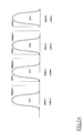
- the distributions are for example roughly Gaussian in shape, and are each one centered around a center threshold voltage value. Thanks to the Gray coding, states that are adjacent (in terms of their distribution of threshold voltage values) have corresponding logic values that differ from each other for only one bit.
- Each word line WL corresponds, according to the present example, to four memory pages, each one corresponding to a specific group of bits. More particularly, a first LSB page includes the LSB stored in the memory cells in even positions (belonging to the first set of memory cells), while a first MSB page includes the MSB stored in the memory cells in even positions. Furthermore, a second LSB page includes the LSB stored in the memory cells in odd positions (belonging to the second set of memory cells), while a second MSB page includes the MSB stored in the memory cells in odd positions. Consequently, the data stored into a single memory cell belongs both to an LSB page and to an MSB page.
- each memory cell 110 is capable to store 2 bits
- each set of 4096 memory cells stores 1024 bytes. Consequently, each memory page is capable to store 512 bytes.
- the matrix 105 includes 2048 word lines WL
- the memory 100 has a total of 8192 memory pages of 512 bytes each.
- the number of bit lines and word lines as well as the size of the memory page may greatly vary, not being a limitation for the present invention.
- the number of memory pages that are associated with a generic word line may be higher, particularly multiples of two, such as eight and so on.
- the flash memory 100 receives an address code ADR for selecting a desired memory page.
- a portion of the address code ADR is supplied to a row decoder 125r, which selects the desired word line WL, as well as the corresponding drain select line DSL and the corresponding source select line SSL.
- Another portion of the address code ADR is supplied to a column decoder 125c; the column decoder 125c connects I/O buffers 140, which are in turn associated with I/O terminals I/O of the flash memory 100, to a page buffer 130.
- a further portion of the address code ADR is used for selecting which one of the (two, in the example) memory pages (the memory page including the MSBs or the memory page including the LSBs of the memory cells of a given set) is addressed.
- the page buffer 130 is exploited as a temporary storage during read/program operations on the memory cells 110 of the selected page.
- the page buffer 130 has a storage capability at least equal to the storage capability of a memory page.
- the column decoder 125c For fitting an internal data parallelism of the flash memory 100 with a maximum external data parallelism, depending on a number p of the I/O terminals I/O (for example, eight or sixteen), the column decoder 125c provides to the page buffer 130 a data word to be written, or provides to the I/O terminals I/O a data word read, in chunks ofp data bits at a time. Particularly, according to the decoding of the received portion of the address code ADR, the column decoder 125c connects desired portions of the page buffer 130 to the I/O terminals I/O.
- the operation of the flash memory 100 is generally managed by a control unit, schematized as a block identified as 135, for example a microcontroller or a finite-state machine.
- the page buffer 130 is adapted to implement operations more complex than a simple page read, a simple page program, and a simple erase operation; in particular, it is assumed that the page buffer 130 is adapted to implement operations such as a cache read operation, and a cache program operation, as will be described in detail later.
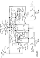
- the page buffer includes a read/program unit 205 for each pair of adjacent bit lines (also each pair of the redundant bit lines is associated with a corresponding read/program unit 205).
- an even bit line BLe and an odd bit line BLo are electrically couplable to a common node SO through respective N-channel MOS transistors 215e and 215o, included in the bit line selector 145.
- the transistors 215e and 215o have the respective drain terminal connected to the corresponding bit lines BLe, BLo, and the source terminals connected to the node SO; the gate terminals of the transistors 215e and 215o are controlled by respective select signals BLSe and BLSo, respectively.
- Two N-channel MOS transistors 220e and 220o are also provided in the bit line selector 145, each one for precharging/discharging the respective bit line BLe and BLo to a biasing voltage VIRPWR (such a precharge/discharge operation is preferably performed before any program operation, as described in the following).
- the transistors 220e and 220o have the source terminals connected to the corresponding bit lines BLe, BLo; the drain terminals of the transistors 220e and 220o are connected together to a terminal for providing the biasing voltage VIRPWR.
- the gate terminals of the transistors 220e, 220o are controlled by respective precharge/ discharge signals DISCHe, DISCHo.
- a P-channel MOS transistor 225 is used for precharging the node SO during certain phases of the page buffer functioning, e.g., at the beginning of a read/program operation.
- the transistor 225 has the drain terminal connected to the node SO, the source terminal connected to a terminal providing the supply voltage Vdd, and the gate terminal controlled by a pre-charge signal PRECHSO_N.
- the read/program unit 205 includes a first latch 230-1 and a second latch 230-2.
- the latch 230-1 is adapted to be employed for the reading of the MSB, for the programming of the MSB, for the loading of data from the outside of the page buffer during a writing operation, for the cache read and for the cache program operations.
- the latch 230-2 is instead adapted to be employed for the reading of the LSB, for the programming of the LSB and the MSB, for the cache read and for the erase operations.
- the latch 230-1 is formed by two inverters INV-1a and INV-1b, connected in a loop with the input terminal of the inverter INV-1a connected to the output terminal of the inverter INV-1b so as to define a node 237-1a, providing a signal SMSB, and the output terminal of the inverter INV-1a connected to the input terminal of the inverter INV-1b so as to define a node 237-1b, providing a signal SMSB_N that is the logic complement of the signal SMSB.
- a further inverter INV-1c has an input terminal connected to the node 237-1a, and an output terminal that is connected to a node 237-1c, providing it the signal MSBREP_N, having the same polarity of the signal SMSB_N.
- An N-channel MOS transistor 240 is used to set the latch 230-1; by "set the latch” there is meant bringing the signal SMSB to the supply voltage VDD.
- the transistor 240 has the drain terminal connected to the node 237-1b, the source terminal connected to ground and the gate terminal controlled by an MSB latch reset signal MSBSET.
- the latch 230-1 is reset (i.e., the signal SMSB is brought to the ground voltage) by means of two N-channel MOS transistors 242 and 244 that are connected in series: the transistor 242 has the drain terminal connected to the node 237-1a and the source terminal connected to the drain terminal of the transistor 244; the source terminal of the transistor 244 is connected to ground.
- the gate terminal of the transistor 244 is controlled by the voltage at the node SO, whereas the gate terminal of the transistor 242 is controlled by a MSB latching or read signal MSBREAD.
- a P-channel MOS transistor 246 is used during a program verify phase for establishing if a MSB program operation has been accomplished in the correct way.
- the transistor 246 has the source terminal connected to a terminal providing the supply voltage Vdd, a gate terminal connected to the node 237-1b, and the drain terminal connected (node MSBVER_N) to a first terminal of a highly-resistive pull down circuit PDWN, the latter having a second terminal connected to ground.
- Said pull down circuit PDWN is placed outside the single read/program unit 205, and its first terminal is commonly connected to transistors 246 in all the other read/write units included in the page buffer 130, in the same way as for the read/write unit herein described.
- An N-channel MOS transistor 248 is used to couple the node 237-1c to the node SO, in order to allow the data transfer from the latch 230-1 to the latch 230-2.
- the transistor 248 has the drain terminal connected to the node SO and the source terminal connected to the node 237-1c; the gate terminal of the transistor 248 is controlled by a data transfer signal DATTRANS.
- N-channel MOS transistors 252 and 254 are used to load data to be written into the first latch 230-1 at the beginning of a program operation.
- the transistors 252 and 254 have respective drain terminals connected to the nodes 237-1a and 237-1b.
- the source terminals of the transistors 252 and 254 are connected together to an I/O data line BITOUT in turn connected to the column decoder 125c, thus establishing a connection between the read/program unit 205 and the I/O buffers 140. Consequently, the I/O data line BITOUT is adapted to provide data to be programmed into the memory cells to the read/program unit, and to provide data that have been read by the read/program unit 205 to the I/O buffers 140.
- the gate terminal of the transistor 252 receives a data load signal DATALOAD_N (whose logic state determines the target value to be loaded into the first latch 230-1) and the gate terminal of the transistor 254 receives a further data load signal DATALOAD (which is the logic complement of the data load signal DATALOAD_N).
- the latch 230-2 is formed by two inverters INV-2a and INV-2b, connected in a loop with the input terminal of the inverter INV-2a connected to the output terminal of the inverter INV-2b so as to define a node 237-2a, providing a signal SLSB, and the output terminal of the inverter INV-2a connected to the input terminal of the inverter INV-2b so as to define a node 237-2b, providing a signal SLSB_N that is the logic complement of the signal SLSB.
- a further inverter INV-2c has an input terminal connected to the node 237-2a, and an output terminal that is connected to a node 237-2c, providing it the signal LSBREP_N, having the same polarity of the signal SLSB_N.
- Three N-channel MOS transistors 256, 258 and 260 are used to set/reset the latch 230-2 and to read/verify the LSB.
- the transistor 256 has the drain terminal connected to the node 237-2a, the source terminal connected to the drain terminal of the transistor 260, and the gate terminal controlled by a first LSB latching or read signal LSBREAD1.
- the transistor 258 has the drain terminal connected to the node 237-2b, the source terminal connected to the drain terminal of the transistor 260, and the gate terminal controlled by a second LSB latching or read signal LSBREAD2.
- the transistor 260 has the source terminal connected to a terminal providing the ground voltage, and the gate terminal connected to the node SO.
- a P-channel MOS transistor 264 is used during verify phases for establishing if an erase operation, or an LSB or an MSB program operation has been accomplished in the correct way.
- the transistor 264 has the source terminal connected to a terminal providing the supply voltage Vdd, a gate terminal connected to the node 237-2b, and the drain terminal connected (node LSBVER_N) to a first terminal of a further highly-resistive pull down circuit (not shown in the Figure for the sake of simplicity), having the same features of the highly-resistive pull down circuit PDWN, and connected to all the read/write units included in the page buffer 130.
- a further N-channel MOS transistor 270 is used to couple the node 237-2c to the node SO, thus to the selected bit line BLe or BLo, during a program operation (as described in greater detail in the following).
- the transistor 270 has the drain terminal connected to the node SO and the source terminal connected to the node 237-2c; the gate terminal of the transistor 270 is controlled by a program signal SLCPROG.
- the read/program unit 205 further includes a four transistors structure that is used for programming the MSB. More particularly, said structure includes four N-channel MOS transistors 272, 274, 276 and 278.
- the transistor 272 has the drain terminal connected to the node SO, the source terminal connected to the drain terminal of the transistor 276, and the gate terminal connected to the gate terminal of the transistor 274 (node 280).
- the transistor 274 has the drain terminal connected to the node SO, the source terminal connected to the drain terminal of the transistor 278, and the gate terminal that is connected to the node 280.
- the transistor 276 has the source terminal connected to the node 237-1c, and the gate terminal connected to the node 237-2c.
- the transistor 278 has the source terminal connected to the node 237-2c, and the gate terminal connected to the node 237-1c.
- the node 280 receives a further program signal MLCPROG.
- Two N-channel MOS transistors 284, 286 are used for providing data to the output of the page buffer 130. More particularly, the transistor 284 has the drain terminal connected to the node 237-1c, the source terminal connected to the I/O data line BITOUT, and the gate terminal controlled by a MSB output signal MSBPASS. The transistor 286 has the drain terminal connected to the node 237-2c, the source terminal connected to the I/O data line BITOUT, and the gate terminal controlled by a LSB output signal LSBPASS.
- a memory page is selected by selecting a given word line WL, and a packet of bit lines BL; for example, if four memory pages of 512 Bytes each exist for each word line, one page corresponding to the LSB of the memory cells in even position, one corresponding to the MSB of the memory cells in even position, one corresponding to the LSB of the memory cells in odd position, and one corresponding to the MSB of the memory cells in odd position, the packet of selected bit lines BL includes the 4096 bit lines in even position or the 4096 bit lines in odd position (it has to be remembered that the data stored into a single memory cell belongs both to an LSB page and to an MSB page).
- a data word stored in the selected memory page is read out and latched into the page buffer 130.
- the data word, temporarily stored in the page buffer 130, is then serially outputted through the I/O terminals I/O in chunks of, e.g., eight or sixteen bits by means of the column decoder 125c.
- the drain select transistor 120d and the source select transistor 120s in the memory cells string to which the cell belongs are turned on, by asserting the drain select line DSL and the source select line SSL (for example, these two lines are brought to a voltage equal to the supply voltage Vdd of the memory); the bit line BL to which there is connected the string of cells containing the memory cell to be read is selected by the bit line selector 145.
- the row decoder 125r biases the word line WL to which the selected memory cell belongs to a reading voltage VREAD2, having a value that is intermediate between the center threshold voltages of the distribution 202 and the voltages of the distribution 203. If the threshold voltage of the selected memory cell 110 is lower than the reading voltage VREAD2, the selected memory cell 110 conducts, thus indicating that the MSB is equal to 1 (it has to be noted that it does not matter if the selected cell belongs to the distribution 201 or to the distribution 202, because both of which correspond to data values in which the MSB is equal to one).
- the selected memory cell 110 does not conduct, thus indicating that the MSB in the stored pair of bit is equal to 0. Thus, it can be appreciated that only one reading operation is necessary to retrieve the value of the MSB.
- a first reading operation is performed by biasing, by means of the row decoder 125r, the word line WL to which the selected memory cell belongs to a reading voltage VREAD1, having a value that is intermediate between the center threshold voltages of the distributions 201 and 202. If the threshold voltage of the selected memory cell 110 is lower than the reading voltage VREAD1, the selected memory cell 110 conducts, thus indicating that it belongs to the distribution 201 (first programming state), and that the LSB is equal to 1. In this case, just one read access is necessary for retrieving the stored LSB.
- the threshold voltage of the selected memory cell 110 is higher than the reading voltage VREAD1, the selected memory cell 110 does not conduct, thus indicating that it does not belong to the distribution 201.
- a second reading operation needs to be perform, biasing the word line WL to which the selected memory cell belongs to a reading voltage VREAD3, having a value that is intermediate between the center threshold voltages of the distributions 203 and 204. If the threshold voltage of the selected memory cell 110 is lower than the reading voltage VREAD3, the selected memory cell 110 conducts, thus indicating that the LSB is equal to 0 (given that the first reading operation has indicated that the threshold voltage is higher than VREAD1). Conversely, if the threshold voltage of the selected memory cell 110 is higher than the reading voltage VREAD3, the selected memory cell 110 does not conduct, thus indicating that it belongs to the distribution 204, and that the LSB is equal to 1.
- the page buffer 130 is operated to execute an MSB read operation rather than an LSB read operation (or vice versa) depending on whether an MSB memory page rather then an LSB memory page has been addressed.
- This is controlled by the control unit 135 that decodes and recognizes the value of the address portion PSEL.
- the control unit 135 generates the signals adapted to drive the execution of all the procedures necessary for performing an LSB read operation (e.g., applying the reading voltages VREAD1 and VREAD3) or for performing an MSB read operation (e.g., applying the reading voltage VREAD2), depending on the value of the address portion PSEL.
- a data word to be written received from outside the memory through the I/O terminals I/O, is loaded into the page buffer 130.
- the data word to be written is received serially in, e.g., eight - or sixteen-bits chunks, and the page buffer 130 is thus replenished with data in a sequence of steps; when the buffer has eventually been filled, the data are written in parallel into the memory cells of a given selected page.
- Memory cells 110 are programmed by Fowler-Nordheim tunneling of electrons into the floating gate.
- the drain select transistor 120d in the memory cells string to which the cell belongs is turned on by asserting the drain select line DSL (for example, bringing this line to the supply voltage Vdd), whereas the source select transistor 120s is kept off by keeping the source select line SSL deasserted (e.g., grounded); the bit line BL to which there is connected the string of cells containing the memory cell to be programmed is selected by the bit line selector 145.
- the row decoder 125r biases the word line WL to which the selected memory cell belongs to a programming voltage VPROG, whose value and evolution in time is a function of the programming state that the memory cell 110 has to assume at the end of the program operation.
- VPROG programming voltage
- the fact that a memory cell 110 is in a particular state is determined by its threshold voltage value, that is in turn determined by the amount of charge present in the corresponding floating gate.
- said amount of charge is in some way proportional to the value and to the rate of increase of the programming voltage VPROG that is applied to the memory cell 110 (e.g., the higher the target threshold voltage value, the higher is the value of the programming voltage VPROG to be applied).
- the remaining word lines WL controlling the gates of the other memory cells of the same string are all brought to a potential relatively high (e.g., approximately 10 V), for reasons that will be described later, but sufficiently lower than the programming voltage not to cause spurious programming. All the other word lines WL (associated with different memory cells strings) are for example kept grounded.
- the bit line BL is kept grounded, so that the drain select transistor 120d is surely kept on; the ground voltage at the bit line, propagating through the drain select transistor and the channel of the memory cells in the string, reaches the channel of the memory cell to be programmed; here, the voltage difference between the control gate (at the programming voltage VPROG) and the channel (close to the ground voltage) experienced by the selected memory cell is sufficient to cause electron tunneling into the floating gate.
- the bit line is biased at a higher potential, for example equal to the memory supply voltage (Vdd, e.g. 3 V), as the drain select line DSL, the drain select transistor 120d turns off. Meanwhile, the voltage of the memory cells string rises.
- the channels of the memory cells of the selected memory cells string thus remain floating, and, thanks to the relatively high voltage (10 V) applied to the word lines WL to which the selected memory cell does not belong, the string channel voltage rises due to the capacitive coupling to a value such that the control gate ⁇ to ⁇ channel voltage difference at the selected memory cell is not sufficient to cause significant electron tunneling, and the memory cell is not programmed.
- the cells 110 of the selected page to be brought to the desired logic value are then programmed, while the other cells 110 are left unchanged.
- more steps are required.
- an LSB program operation is firstly performed: if the selected memory cell 110 has to be programmed in such a way to have an LSB value that is equal to 0, the programming voltage VPROG that is applied to the selected word line WL is such as to bring the threshold voltage of the selected memory cell to the distribution 202 (i.e., to the second state). Otherwise, the threshold voltage of the selected memory cell 110 remains in the first distribution (first state, or erased state). Having executed the LSB program operation, the whole program operation is completed by means of the programming of the MSB value.
- the threshold voltage of the memory cell remains at the value it reached in the previous step (i.e., belonging to the distribution 201 if LSB is 1, and belonging to the distribution 202 if LSB is 0).
- the programming voltage VPROG is such as to bring the threshold voltage of the selected memory cell to the distribution 204 (i.e., to the fourth state) if the LSB is equal to 1 (i.e., if the threshold voltage before the MSB programming belonged to the distribution 201); conversely, if the LSB is equal to 0 (i.e., if the threshold voltage before the MSB programming belonged to the distribution 202), the programming voltage VPROG is such as to bring the threshold voltage of the selected memory cell to the distribution 203 (i.e., to the third state).
- a possible program operation includes the repetition of a plurality of steps, at each step increasing the programming voltage VPROGR (up to a maximum value, e.g. 20V), and, after the application of the programming voltage, the execution of a verify phase for determining if the desired threshold voltage value has been reached.
- the erase operation has the purpose of bringing a block of memory cells 110 back to the erased state (logic value "11"), wherein by memory cells block there is intended a group of memory cells 110 corresponding to all the word lines WL of a string.
- the semiconductor well including all the cells of the matrix 105 is biased to a relatively high erase voltage VERASE (e.g., 20 Volts) by means of an erase control circuit, not shown in the Figures, and all the bit lines BL of the matrix 105 are kept floating.
- the row decoder 125r biases the word lines WL corresponding to the block to the ground voltage, while the remaining word lines WL of the matrix 105 are kept floating.
- the drain select lines DSL and the source select lines SSL of the block are kept floating (but they are precharged at about the supply voltage Vdd before the well is biased to the erase voltage VERASE), while the remaining are grounded.
- each memory cell 110 included in the selected block is biased in such a way to trigger the removal (by means of tunneling effect) of the electrical charge possibly stored in its floating gate.
- the erase operation is in the practice more complex, including erase verify phases and soft program operations.
- each pair of bit lines and a corresponding read/program unit 205 is accomplished by means of a connection with the circuital node SO included in the latter.
- the node SO absolve a variety of functions, regarding the operations performed by the read/program unit 205 on a selected memory cell 110 connected to a bit line coupled thereto.
- the node SO is adapted to be charged to the supply voltage Vdd, and to be discharged toward the ground voltage if certain conditions occur.
- the node SO is firstly precharged to the supply voltage Vdd, and then it is forced to assume a voltage value equal to that of the coupled bit line. In this way, the node SO discharges or not depending on the conductivity (i.e., the programming state) of the selected memory cell connected to the bit line. Consequently, the node SO remains floating at the supply voltage Vdd if the selected memory cell is not conductive.
- the node SO is firstly precharged to the supply voltage Vdd. Then, the node SO is forced to discharge if the selected memory cell 110 has to be programmed. Conversely, the node SO is maintained to the supply voltage Vdd if the selected memory cell 110 has not to be programmed.
- precharging/discharging the circuital node SO are also performed whenever a transfer of data from the latch 230-1 to the latch 230-2 is requested.
- the circuit node SO of each read/program unit 205 is precharged to the supply voltage Vdd. Said voltage value is maintained by the node SO in a floating condition, thanks to the unavoidable parasitic capacitances associated with conductive signal line (e.g., formed from a metallic layer) that physically realizes the node SO in the chip.
- conductive signal line e.g., formed from a metallic layer
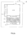
- FIG. 3A a simplified topological top plan view of the memory device 100 is illustrated in a schematic view according to an embodiment of the present invention.
- FIG. 1 there is depicted an exemplary arrangement of the most important circuital blocks included in the memory device 100 (and previously described) on a semiconductor chip 300.
- the memory matrix 105 is illustrated as a rectangular area, with the row decoder 125r positioned adjacently to the matrix left side, and the area of the bit line selector 145 that is positioned adjacently to the bottom side of the memory matrix.
- the page buffer 130 occupies the area placed directly under that of the bit line selector 145, and the column decoder 125c is placed directly under the page buffer 130. It has to be noted that the present description of the arrangement of the various circuital blocks included in the memory device refers to a case that is to be considered as typical for a NAND memory.
- the page buffer 130 includes a plurality of read/program units 205. Each unit 205 is connected to a pair of bit lines (BLe, BLo) of the memory matrix 105.
- the Figure 3A further includes, for the sake of clarity, two perpendicular arrows X, Y defining two reference directions.
- the arrow X defines a horizontal direction (the direction along which the word lines extend), while the arrow Y defines a vertical direction (the direction of extension of the bit lines).
- each read/program unit 205(i) is crossed by five conductive tracks, running in the Y direction.
- SL signal levels
- the node SO of a read/program unit 205(i), and thus the corresponding conductive track SOi may have to be kept at the supply voltage Vdd in a floating condition.
- Said floating condition is characterized by being strongly influenceable by the capacitive couplings between adjacent conductive tracks, do to the unavoidable presence of parasitic capacitances (not shown in the Figure). For example, if a memory cell 110 selected for reading has been ascertained to be programmed, the node SO (and the corresponding conductive track SOi) of the associated read/program unit 205(i) has to remain at the supply voltage value Vdd.
- the voltage of the conductive track SOi in consideration will be undesirably affected, dropping by a certain (hardly predictable) amount. If said voltage decrease exceeds the trigger threshold of the latch 230-2 included in the read/program unit 205(i), the voltage value of the node SOi will not be able to cause the latch to switch, thus providing a wrong read operation result.
- the conductive tracks whose voltages mainly affect the voltage value of the node SO of a generic read/program unit are the conductive tracks forming the circuit nodes SO of the remaining read/program units of the group, because they run essentially in parallel along the Y direction.
- capacitors may be deliberately provided for in the circuit design, connected to the conductive tracks SOi themselves.
- adding several capacitors implies an excessive waste of silicon area.
- Another solution for equalizing the parasitic capacitances of the different conductive track SOi consists of extending each conductive track SOi so that all the tracks SOi have an essentially equal length along the Y direction.
- each conductive track SOi in the Y direction so that it traverses the whole area occupied by the group of stacked read/program unit 205(i)
- the SL increases, and becomes equal to eight in the example at issue. This may pose problems in terms of space constraints: accommodating eight conductive tracks in the pitch of eight bit lines is in fact not easy, or it may even be impractical.
- a possible solution consists of providing a shared single conductive track BITOUT per each stack of four read/program units 205(i).
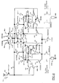
- a column-selection N-channel transistor 410 may be introduced within the structure of the generic read/program unit 205 previously described.
- the column-selection transistor 410 has the drain terminal connected to the source terminals of the transistors 252, 254, 284, 286, the gate terminal that receives a column selection signal YDATAPASS, and the source terminal that is connected to a conductive track BITOUT that is common to all the read/program units 205(i) belonging to the stack.
- the read/program units 205(i) have to output data to the column decoder, one column selection transistor 410 among the four of the four read/program units of the group is activated at a time by the column decoding signal YDATAPASS.
- FIG. 3C a more detailed view of a stack of four read/program units 205(i), each one including a corresponding column selection transistor 410, and of the corresponding conductive tracks are illustrated according to an embodiment of the present invention.
- each one of the four conductive tracks SOi defines a winding path running from the memory matrix 105 to the column decoder 125c, swinging in the X and Y directions, and is "twisted", “intertwined” with the other conductive tracks SOi. More particularly, in an exemplary but not limitative embodiment of the present invention, indicating as X1, X2, X3, X4 four different positions from the left to the right along the X direction, all the conductive tracks SOi, in their path from the memory matrix 105 to the column decoder 125c, occupy all of said four positions X1, X2, X3, X4, in an essentially similar way.
- the conductive track SO1 it can be regarded as subdivided in four segments, a first segment, in correspondence of the area of the read/program unit 205(1), occupying the position X1, a second segment, connected to the first segment, in correspondence of the read/program unit 205(2), occupying the position X4, a third segment, connected to the second segment, in correspondence of the read/program unit 205(3), occupying the position X3, and a fourth segment, connected to the third segment, in correspondence of the read/program unit 205(4), occupying the position X2.
- the conductive tracks SOi of a stack of read/program units exhibit essentially the same parasitic capacitances (having the same lengths), and, thanks to the "intertwined" arrangement, they experience essentially equal capacitive couplings.
- the single conductive track BITOUT that is common to all the read/program units 205(i) belonging to a stack preferably runs in the center of the stack, between the positions X2 and X3; in this way, the structure is essentially symmetric.
- metal 1 may be formed in metal 1 in metal 1
- metal 3 being a metallic layer patterned to define conductive tracks running essentially in the same direction as those formed from the metal 1: the nodes SO corresponding to the conductive tracks SOi are thus kept isolated during the read operations. In fact, the segments of the conductive tracks SOi that are realized in metal 3 are shielded from the conductive track BITOUT, while the capacitive couplings among metal 1 and metal 3 are negligible.
- Figure 3D shows a very simplified cross-sectional view of the exemplary read program unit 205(4) shown in the Figure 3C, along the line IIID-IIID.
- the conductive tracks SO4 (corresponding to the position X1) and SO3 (corresponding to the position X4) are photolithographically realized from a first layer of metal 310
- the conductive tracks SO1 (corresponding to the position X2), SO2 (corresponding to the position X3) and the conductive track BITOUT are photolithographically realized from a second layer of metal 310.
- Figure 3E is a very simplified cross-sectional view of a portion of read program units 205(1) and 205(2) shown in the Figure 3C, along the line IIIE-IIIE.
- the segment of the conductive track SO4 belonging to the read/program unit 205(1) corresponds to the position X4, and thus is realized from the first layer of metal 310.
- the segment of the conductive track SO4 belonging to the read/program unit 205(2) corresponds to the position X3, and thus is realized from the second layer of metal 320.
- the connection of this two segments belonging to different layers of metal is realized by means of a via 330.
Landscapes
- Engineering & Computer Science (AREA)
- Computer Hardware Design (AREA)
- Microelectronics & Electronic Packaging (AREA)
- Read Only Memory (AREA)
Priority Applications (3)
| Application Number | Priority Date | Filing Date | Title |
|---|---|---|---|
| DE602005006791T DE602005006791D1 (de) | 2005-07-28 | 2005-07-28 | Halbleiterspeicher und sein Seitenpufferspeicher mit verbessertem Layout |
| EP05106973A EP1748443B1 (fr) | 2005-07-28 | 2005-07-28 | Mémoire à semiconducteurs avec tampon de page ayant un agencement amélioré |
| US11/459,831 US7408819B2 (en) | 2005-07-28 | 2006-07-25 | Semiconductor memory device with a page buffer having an improved layout arrangement |
Applications Claiming Priority (1)
| Application Number | Priority Date | Filing Date | Title |
|---|---|---|---|
| EP05106973A EP1748443B1 (fr) | 2005-07-28 | 2005-07-28 | Mémoire à semiconducteurs avec tampon de page ayant un agencement amélioré |
Publications (2)
| Publication Number | Publication Date |
|---|---|
| EP1748443A1 true EP1748443A1 (fr) | 2007-01-31 |
| EP1748443B1 EP1748443B1 (fr) | 2008-05-14 |
Family
ID=35520515
Family Applications (1)
| Application Number | Title | Priority Date | Filing Date |
|---|---|---|---|
| EP05106973A Expired - Lifetime EP1748443B1 (fr) | 2005-07-28 | 2005-07-28 | Mémoire à semiconducteurs avec tampon de page ayant un agencement amélioré |
Country Status (3)
| Country | Link |
|---|---|
| US (1) | US7408819B2 (fr) |
| EP (1) | EP1748443B1 (fr) |
| DE (1) | DE602005006791D1 (fr) |
Families Citing this family (1)
| Publication number | Priority date | Publication date | Assignee | Title |
|---|---|---|---|---|
| DE602005006791D1 (de) * | 2005-07-28 | 2008-06-26 | St Microelectronics Srl | Halbleiterspeicher und sein Seitenpufferspeicher mit verbessertem Layout |
Citations (7)
| Publication number | Priority date | Publication date | Assignee | Title |
|---|---|---|---|---|
| US4418399A (en) * | 1979-12-13 | 1983-11-29 | Fujitsu Limited | Semiconductor memory system |
| US5625590A (en) * | 1994-12-19 | 1997-04-29 | Samsung Electronics Co., Ltd. | Nonvolatile semiconductor memory |
| US6377507B1 (en) * | 2001-04-06 | 2002-04-23 | Integrated Memory Technologies, Inc. | Non-volatile memory device having high speed page mode operation |
| US20020186591A1 (en) * | 2001-06-11 | 2002-12-12 | Sumsung Electronics Co,. Ltd. | Semiconductor memory device having memory cell arrays capable of accomplishing random access |
| US20040062099A1 (en) * | 2000-11-01 | 2004-04-01 | Kabushiki Kaisha Toshiba | Fail number detecting circuit of flash memory |
| DE10344021A1 (de) * | 2002-12-09 | 2004-07-15 | Samsung Electronics Co., Ltd., Suwon | Nichtflüchtiger Speicherbaustein, Programmiervorrichtung und Programmierverfahren |
| US20040240268A1 (en) * | 2003-05-28 | 2004-12-02 | Kim In-Young | Semiconductor memory device having flexible column redundancy scheme |
Family Cites Families (1)
| Publication number | Priority date | Publication date | Assignee | Title |
|---|---|---|---|---|
| DE602005006791D1 (de) * | 2005-07-28 | 2008-06-26 | St Microelectronics Srl | Halbleiterspeicher und sein Seitenpufferspeicher mit verbessertem Layout |
-
2005
- 2005-07-28 DE DE602005006791T patent/DE602005006791D1/de not_active Expired - Lifetime
- 2005-07-28 EP EP05106973A patent/EP1748443B1/fr not_active Expired - Lifetime
-
2006
- 2006-07-25 US US11/459,831 patent/US7408819B2/en active Active
Patent Citations (7)
| Publication number | Priority date | Publication date | Assignee | Title |
|---|---|---|---|---|
| US4418399A (en) * | 1979-12-13 | 1983-11-29 | Fujitsu Limited | Semiconductor memory system |
| US5625590A (en) * | 1994-12-19 | 1997-04-29 | Samsung Electronics Co., Ltd. | Nonvolatile semiconductor memory |
| US20040062099A1 (en) * | 2000-11-01 | 2004-04-01 | Kabushiki Kaisha Toshiba | Fail number detecting circuit of flash memory |
| US6377507B1 (en) * | 2001-04-06 | 2002-04-23 | Integrated Memory Technologies, Inc. | Non-volatile memory device having high speed page mode operation |
| US20020186591A1 (en) * | 2001-06-11 | 2002-12-12 | Sumsung Electronics Co,. Ltd. | Semiconductor memory device having memory cell arrays capable of accomplishing random access |
| DE10344021A1 (de) * | 2002-12-09 | 2004-07-15 | Samsung Electronics Co., Ltd., Suwon | Nichtflüchtiger Speicherbaustein, Programmiervorrichtung und Programmierverfahren |
| US20040240268A1 (en) * | 2003-05-28 | 2004-12-02 | Kim In-Young | Semiconductor memory device having flexible column redundancy scheme |
Also Published As
| Publication number | Publication date |
|---|---|
| EP1748443B1 (fr) | 2008-05-14 |
| US7408819B2 (en) | 2008-08-05 |
| US20070025148A1 (en) | 2007-02-01 |
| DE602005006791D1 (de) | 2008-06-26 |
Similar Documents
| Publication | Publication Date | Title |
|---|---|---|
| US7336538B2 (en) | Page buffer circuit and method for multi-level NAND programmable memories | |
| US7471576B2 (en) | Method of transferring data in an electrically programmable memory | |
| CN101714409B (zh) | 具有改进的部分页编程能力的非易失性存储器和控制 | |
| US7499332B2 (en) | Circuit and method for electrically programming a non-volatile semiconductor memory via an additional programming pulse after verification | |
| US7630238B2 (en) | Page buffer for multi-level NAND electrically-programmable semiconductor memories | |
| US8228729B2 (en) | Structure and method for shuffling data within non-volatile memory devices | |
| KR101160748B1 (ko) | 불휘발성 반도체 기억 장치 및 메모리 시스템 | |
| US20100309719A1 (en) | Folding Data Stored in Binary Format Into Multi-State Format Within Non-Volatile Memory Devices | |
| WO2014210424A2 (fr) | Nouvelle architecture de réseau non-et destinée à plusieurs programmations et lectures simultanées | |
| US20020057596A1 (en) | Semiconductor memory device and storage method thereof | |
| CN101512668A (zh) | 对于快闪存储器中的循环效应的伪随机及命令驱动位补偿及其方法 | |
| US8189394B2 (en) | Page buffer circuit of nonvolatile memory device and method of operating the same | |
| EP1610343B1 (fr) | Tampon de page amélioré pour un dispositif mémoire programmable | |
| EP1748443B1 (fr) | Mémoire à semiconducteurs avec tampon de page ayant un agencement amélioré | |
| EP1748445B1 (fr) | Mémoire tampon de pages pour mémoire programmable du type NAND a multiples niveaux | |
| KR101227368B1 (ko) | 낸드 플래시 메모리 소자의 프로그래밍 방법 및 데이터읽기 방법. | |
| US20070268732A1 (en) | Method and apparatus providing non-volatile memory with reduced cell capacitive coupling | |
| EP1748446A1 (fr) | Programmation de deux pages |
Legal Events
| Date | Code | Title | Description |
|---|---|---|---|
| PUAI | Public reference made under article 153(3) epc to a published international application that has entered the european phase |
Free format text: ORIGINAL CODE: 0009012 |
|
| AK | Designated contracting states |
Kind code of ref document: A1 Designated state(s): AT BE BG CH CY CZ DE DK EE ES FI FR GB GR HU IE IS IT LI LT LU LV MC NL PL PT RO SE SI SK TR |
|
| AX | Request for extension of the european patent |
Extension state: AL BA HR MK YU |
|
| 17P | Request for examination filed |
Effective date: 20070419 |
|
| 17Q | First examination report despatched |
Effective date: 20070518 |
|
| AKX | Designation fees paid |
Designated state(s): DE FR GB IT |
|
| GRAP | Despatch of communication of intention to grant a patent |
Free format text: ORIGINAL CODE: EPIDOSNIGR1 |
|
| GRAS | Grant fee paid |
Free format text: ORIGINAL CODE: EPIDOSNIGR3 |
|
| GRAA | (expected) grant |
Free format text: ORIGINAL CODE: 0009210 |
|
| AK | Designated contracting states |
Kind code of ref document: B1 Designated state(s): DE FR GB IT |
|
| REG | Reference to a national code |
Ref country code: GB Ref legal event code: FG4D |
|
| REF | Corresponds to: |
Ref document number: 602005006791 Country of ref document: DE Date of ref document: 20080626 Kind code of ref document: P |
|
| PLBE | No opposition filed within time limit |
Free format text: ORIGINAL CODE: 0009261 |
|
| STAA | Information on the status of an ep patent application or granted ep patent |
Free format text: STATUS: NO OPPOSITION FILED WITHIN TIME LIMIT |
|
| 26N | No opposition filed |
Effective date: 20090217 |
|
| REG | Reference to a national code |
Ref country code: FR Ref legal event code: ST Effective date: 20090331 |
|
| PG25 | Lapsed in a contracting state [announced via postgrant information from national office to epo] |
Ref country code: IT Free format text: LAPSE BECAUSE OF FAILURE TO SUBMIT A TRANSLATION OF THE DESCRIPTION OR TO PAY THE FEE WITHIN THE PRESCRIBED TIME-LIMIT Effective date: 20080514 Ref country code: FR Free format text: LAPSE BECAUSE OF NON-PAYMENT OF DUE FEES Effective date: 20080731 |
|
| GBPC | Gb: european patent ceased through non-payment of renewal fee |
Effective date: 20090728 |
|
| PG25 | Lapsed in a contracting state [announced via postgrant information from national office to epo] |
Ref country code: GB Free format text: LAPSE BECAUSE OF NON-PAYMENT OF DUE FEES Effective date: 20090728 |
|
| REG | Reference to a national code |
Ref country code: DE Ref legal event code: R082 Ref document number: 602005006791 Country of ref document: DE Representative=s name: KLUNKER, SCHMITT-NILSON, HIRSCH, DE |
|
| REG | Reference to a national code |
Ref country code: DE Ref legal event code: R082 Ref document number: 602005006791 Country of ref document: DE Representative=s name: SCHMITT-NILSON SCHRAUD WAIBEL WOHLFROM PATENTA, DE Effective date: 20131209 Ref country code: DE Ref legal event code: R081 Ref document number: 602005006791 Country of ref document: DE Owner name: MICRON TECHNOLOGY, INC., US Free format text: FORMER OWNER: STMICROELECTRONICS S.R.L., HYNIX SEMICONDUCTOR INC., , KR Effective date: 20131209 Ref country code: DE Ref legal event code: R081 Ref document number: 602005006791 Country of ref document: DE Owner name: HYNIX SEMICONDUCTOR INC., KR Free format text: FORMER OWNER: STMICROELECTRONICS S.R.L., HYNIX SEMICONDUCTOR INC., , KR Effective date: 20131209 Ref country code: DE Ref legal event code: R082 Ref document number: 602005006791 Country of ref document: DE Representative=s name: KLUNKER, SCHMITT-NILSON, HIRSCH, DE Effective date: 20131209 Ref country code: DE Ref legal event code: R081 Ref document number: 602005006791 Country of ref document: DE Owner name: MICRON TECHNOLOGY, INC., BOISE, US Free format text: FORMER OWNER: STMICROELECTRONICS S.R.L., HYNIX SEMICONDUCTOR INC., , KR Effective date: 20131209 Ref country code: DE Ref legal event code: R081 Ref document number: 602005006791 Country of ref document: DE Owner name: HYNIX SEMICONDUCTOR INC., ICHEON, KR Free format text: FORMER OWNER: STMICROELECTRONICS S.R.L., HYNIX SEMICONDUCTOR INC., , KR Effective date: 20131209 Ref country code: DE Ref legal event code: R081 Ref document number: 602005006791 Country of ref document: DE Owner name: MICRON TECHNOLOGY, INC., BOISE, US Free format text: FORMER OWNERS: STMICROELECTRONICS S.R.L., AGRATE BRIANZA, MAILAND/MILANO, IT; HYNIX SEMICONDUCTOR INC., ICHEON, KYONGGI, KR Effective date: 20131209 Ref country code: DE Ref legal event code: R081 Ref document number: 602005006791 Country of ref document: DE Owner name: MICRON TECHNOLOGY, INC., BOISE, US Free format text: FORMER OWNERS: STMICROELECTRONICS S.R.L., AGRATE BRIANZA, IT; HYNIX SEMICONDUCTOR INC., ICHEON, KYONGGI, KR Effective date: 20131209 |
|
| REG | Reference to a national code |
Ref country code: DE Ref legal event code: R082 Ref document number: 602005006791 Country of ref document: DE Representative=s name: KLUNKER, SCHMITT-NILSON, HIRSCH, DE |
|
| REG | Reference to a national code |
Ref country code: DE Ref legal event code: R082 Ref document number: 602005006791 Country of ref document: DE Representative=s name: SCHMITT-NILSON SCHRAUD WAIBEL WOHLFROM PATENTA, DE Effective date: 20140828 Ref country code: DE Ref legal event code: R081 Ref document number: 602005006791 Country of ref document: DE Owner name: MICRON TECHNOLOGY, INC., BOISE, US Free format text: FORMER OWNERS: HYNIX SEMICONDUCTOR INC., ICHEON, KYONGGI, KR; MICRON TECHNOLOGY, INC., BOISE, ID., US Effective date: 20140828 Ref country code: DE Ref legal event code: R082 Ref document number: 602005006791 Country of ref document: DE Representative=s name: KLUNKER, SCHMITT-NILSON, HIRSCH, DE Effective date: 20140828 Ref country code: DE Ref legal event code: R081 Ref document number: 602005006791 Country of ref document: DE Owner name: MICRON TECHNOLOGY, INC., BOISE, US Free format text: FORMER OWNER: HYNIX SEMICONDUCTOR INC., MICRON TECHNOLOGY, INC., , US Effective date: 20140828 |
|
| REG | Reference to a national code |
Ref country code: DE Ref legal event code: R082 Ref document number: 602005006791 Country of ref document: DE Representative=s name: SCHMITT-NILSON SCHRAUD WAIBEL WOHLFROM PATENTA, DE |
|
| PGFP | Annual fee paid to national office [announced via postgrant information from national office to epo] |
Ref country code: DE Payment date: 20240730 Year of fee payment: 20 |
|
| REG | Reference to a national code |
Ref country code: DE Ref legal event code: R071 Ref document number: 602005006791 Country of ref document: DE |