EP1748473A2 - Transistor de mémoire non-volatile avec des sites de piégeage de charges distribués - Google Patents
Transistor de mémoire non-volatile avec des sites de piégeage de charges distribués Download PDFInfo
- Publication number
- EP1748473A2 EP1748473A2 EP06118057A EP06118057A EP1748473A2 EP 1748473 A2 EP1748473 A2 EP 1748473A2 EP 06118057 A EP06118057 A EP 06118057A EP 06118057 A EP06118057 A EP 06118057A EP 1748473 A2 EP1748473 A2 EP 1748473A2
- Authority
- EP
- European Patent Office
- Prior art keywords
- charge
- tunnelling
- storage medium
- volatile memory
- memory device
- Prior art date
- Legal status (The legal status is an assumption and is not a legal conclusion. Google has not performed a legal analysis and makes no representation as to the accuracy of the status listed.)
- Withdrawn
Links
Images


Classifications
-
- H—ELECTRICITY
- H10—SEMICONDUCTOR DEVICES; ELECTRIC SOLID-STATE DEVICES NOT OTHERWISE PROVIDED FOR
- H10D—INORGANIC ELECTRIC SEMICONDUCTOR DEVICES
- H10D30/00—Field-effect transistors [FET]
- H10D30/60—Insulated-gate field-effect transistors [IGFET]
- H10D30/68—Floating-gate IGFETs
- H10D30/681—Floating-gate IGFETs having only two programming levels
-
- B—PERFORMING OPERATIONS; TRANSPORTING
- B82—NANOTECHNOLOGY
- B82Y—SPECIFIC USES OR APPLICATIONS OF NANOSTRUCTURES; MEASUREMENT OR ANALYSIS OF NANOSTRUCTURES; MANUFACTURE OR TREATMENT OF NANOSTRUCTURES
- B82Y10/00—Nanotechnology for information processing, storage or transmission, e.g. quantum computing or single electron logic
-
- G—PHYSICS
- G11—INFORMATION STORAGE
- G11C—STATIC STORES
- G11C16/00—Erasable programmable read-only memories
- G11C16/02—Erasable programmable read-only memories electrically programmable
- G11C16/04—Erasable programmable read-only memories electrically programmable using variable threshold transistors, e.g. FAMOS
- G11C16/0466—Erasable programmable read-only memories electrically programmable using variable threshold transistors, e.g. FAMOS comprising cells with charge storage in an insulating layer, e.g. metal-nitride-oxide-silicon [MNOS], silicon-oxide-nitride-oxide-silicon [SONOS]
- G11C16/0475—Erasable programmable read-only memories electrically programmable using variable threshold transistors, e.g. FAMOS comprising cells with charge storage in an insulating layer, e.g. metal-nitride-oxide-silicon [MNOS], silicon-oxide-nitride-oxide-silicon [SONOS] comprising two or more independent storage sites which store independent data
-
- H—ELECTRICITY
- H10—SEMICONDUCTOR DEVICES; ELECTRIC SOLID-STATE DEVICES NOT OTHERWISE PROVIDED FOR
- H10D—INORGANIC ELECTRIC SEMICONDUCTOR DEVICES
- H10D30/00—Field-effect transistors [FET]
- H10D30/60—Insulated-gate field-effect transistors [IGFET]
- H10D30/68—Floating-gate IGFETs
- H10D30/6891—Floating-gate IGFETs characterised by the shapes, relative sizes or dispositions of the floating gate electrode
- H10D30/6893—Floating-gate IGFETs characterised by the shapes, relative sizes or dispositions of the floating gate electrode wherein the floating gate has multiple non-connected parts, e.g. multi-particle floating gate
-
- H—ELECTRICITY
- H10—SEMICONDUCTOR DEVICES; ELECTRIC SOLID-STATE DEVICES NOT OTHERWISE PROVIDED FOR
- H10D—INORGANIC ELECTRIC SEMICONDUCTOR DEVICES
- H10D30/00—Field-effect transistors [FET]
- H10D30/60—Insulated-gate field-effect transistors [IGFET]
- H10D30/69—IGFETs having charge trapping gate insulators, e.g. MNOS transistors
-
- H—ELECTRICITY
- H10—SEMICONDUCTOR DEVICES; ELECTRIC SOLID-STATE DEVICES NOT OTHERWISE PROVIDED FOR
- H10D—INORGANIC ELECTRIC SEMICONDUCTOR DEVICES
- H10D64/00—Electrodes of devices having potential barriers
- H10D64/01—Manufacture or treatment
- H10D64/031—Manufacture or treatment of data-storage electrodes
- H10D64/035—Manufacture or treatment of data-storage electrodes comprising conductor-insulator-conductor-insulator-semiconductor structures
-
- H—ELECTRICITY
- H10—SEMICONDUCTOR DEVICES; ELECTRIC SOLID-STATE DEVICES NOT OTHERWISE PROVIDED FOR
- H10D—INORGANIC ELECTRIC SEMICONDUCTOR DEVICES
- H10D64/00—Electrodes of devices having potential barriers
- H10D64/01—Manufacture or treatment
- H10D64/031—Manufacture or treatment of data-storage electrodes
- H10D64/037—Manufacture or treatment of data-storage electrodes comprising charge-trapping insulators
Definitions
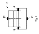
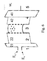
- Figure 1 is a drawing illustrating a schematic cross-section of a non-volatile memory device.
- a non-volatile memory device which comprises a charge supply region 1, a charge storage medium 3 comprising discrete storage sites isolated from each other, an insulating barrier 2 extending between the charge supply region and the charge storage medium.
- a mechanism 4, 5 is provided for establishing an electric field over the insulating barrier 2 and for establishing a difference in electrochemical potential over the insulating barrier for tunnelling charge carriers (negative or positive, e.g. electrons or holes, respectively) from the charge supply region 1 to the charge storage medium 3.
- the charge supply region provides charge carriers of opposite polarity, e.g. electrons and holes.
- the presence of the thicker second portion 22 of the insulating barrier does increase the physical thickness of the insulating barrier 2, thereby providing an additional potential energy barrier for the charge stored in the charge storage medium to tunnel from the charge storage medium 3 towards the charge supply region 1. So the presence of the second portion 22 of the insulating barrier is a first factor that enhances data retention of the non-volatile memory device.
- Erasing of the memory device is realized by applying a high voltage to the control region 5 with respect to the supply region 1, but having opposite polarity as compared to the voltage applied to the control region 5 when writing the non-volatile memory device.
- This high voltage difference must be sufficient for tunnelling of carriers from the charge supply region 1 through the insulating barrier 2 into the charge storage medium 3 in an energy band, other than the energy band for tunnelling of carriers when programming the memory device.
- the carriers are thus of a polarity opposite to the polarity of carriers tunnelling from the charge supply region 1 to the charge storage medium 3 when writing the non-volatile memory device.
Landscapes
- Engineering & Computer Science (AREA)
- Chemical & Material Sciences (AREA)
- Nanotechnology (AREA)
- Microelectronics & Electronic Packaging (AREA)
- Physics & Mathematics (AREA)
- Mathematical Physics (AREA)
- Theoretical Computer Science (AREA)
- Crystallography & Structural Chemistry (AREA)
- Non-Volatile Memory (AREA)
- Semiconductor Memories (AREA)
Priority Applications (1)
| Application Number | Priority Date | Filing Date | Title |
|---|---|---|---|
| EP06118057A EP1748473A3 (fr) | 2005-07-28 | 2006-07-28 | Transistor de mémoire non-volatile avec des sites de piégeage de charges distribués |
Applications Claiming Priority (3)
| Application Number | Priority Date | Filing Date | Title |
|---|---|---|---|
| US70363905P | 2005-07-28 | 2005-07-28 | |
| EP05112170A EP1748472A1 (fr) | 2005-07-28 | 2005-12-14 | Transistor de mémoire non-volatile |
| EP06118057A EP1748473A3 (fr) | 2005-07-28 | 2006-07-28 | Transistor de mémoire non-volatile avec des sites de piégeage de charges distribués |
Publications (2)
| Publication Number | Publication Date |
|---|---|
| EP1748473A2 true EP1748473A2 (fr) | 2007-01-31 |
| EP1748473A3 EP1748473A3 (fr) | 2009-04-01 |
Family
ID=37200750
Family Applications (1)
| Application Number | Title | Priority Date | Filing Date |
|---|---|---|---|
| EP06118057A Withdrawn EP1748473A3 (fr) | 2005-07-28 | 2006-07-28 | Transistor de mémoire non-volatile avec des sites de piégeage de charges distribués |
Country Status (1)
| Country | Link |
|---|---|
| EP (1) | EP1748473A3 (fr) |
Cited By (2)
| Publication number | Priority date | Publication date | Assignee | Title |
|---|---|---|---|---|
| EP2063459A1 (fr) | 2007-11-22 | 2009-05-27 | Interuniversitair Microelektronica Centrum vzw | Diélectrique de bloquage pour un dispositif de mémoire non-volatile doté d'une grille de contrôle métallique ou du type p |
| CN113471205A (zh) * | 2021-06-30 | 2021-10-01 | 沈阳工业大学 | 一种非易失性可重置双向开关装置及其制造方法 |
Family Cites Families (3)
| Publication number | Priority date | Publication date | Assignee | Title |
|---|---|---|---|---|
| EP1253646B1 (fr) * | 2001-04-27 | 2011-09-14 | Imec | Barrière isolante pour dispositif de mémoire rémanente. |
| KR100446632B1 (ko) * | 2002-10-14 | 2004-09-04 | 삼성전자주식회사 | 비휘발성 sonsnos 메모리 |
| EP1487013A3 (fr) * | 2003-06-10 | 2006-07-19 | Samsung Electronics Co., Ltd. | Cellule mémoire de type SONOS et son procédé de fabrication |
-
2006
- 2006-07-28 EP EP06118057A patent/EP1748473A3/fr not_active Withdrawn
Cited By (4)
| Publication number | Priority date | Publication date | Assignee | Title |
|---|---|---|---|---|
| EP2063459A1 (fr) | 2007-11-22 | 2009-05-27 | Interuniversitair Microelektronica Centrum vzw | Diélectrique de bloquage pour un dispositif de mémoire non-volatile doté d'une grille de contrôle métallique ou du type p |
| US8119511B2 (en) | 2007-11-22 | 2012-02-21 | Imec | Non-volatile memory device with improved immunity to erase saturation and method for manufacturing same |
| CN113471205A (zh) * | 2021-06-30 | 2021-10-01 | 沈阳工业大学 | 一种非易失性可重置双向开关装置及其制造方法 |
| CN113471205B (zh) * | 2021-06-30 | 2023-11-03 | 沈阳工业大学 | 一种非易失性可重置双向开关装置及其制造方法 |
Also Published As
| Publication number | Publication date |
|---|---|
| EP1748473A3 (fr) | 2009-04-01 |
Similar Documents
| Publication | Publication Date | Title |
|---|---|---|
| US7626226B2 (en) | Method for improving erase saturation in non-volatile memory devices and devices obtained thereof | |
| KR101208785B1 (ko) | 인터폴리 전하 트래핑 구조를 갖는 플로팅 게이트 메모리 디바이스 | |
| US7560767B2 (en) | Nonvolatile semiconductor memory device | |
| TWI388052B (zh) | 具有分離閘極及阻擋層之記憶元件 | |
| CN100446258C (zh) | 存储单元,存储单元装置和制造方法 | |
| JP5149539B2 (ja) | 半導体装置 | |
| US10497710B2 (en) | Split-gate flash cell formed on recessed substrate | |
| US9041145B2 (en) | Semiconductor device | |
| TWI409940B (zh) | 抑制反及閘電荷捕捉記憶體邊緣電場干擾之方法與裝置 | |
| US8466505B2 (en) | Multi-level flash memory cell capable of fast programming | |
| EP1918984A2 (fr) | Dispositif de piégeage de charge à canal cylindrique et procédé de fabrication correspondant | |
| US12550382B2 (en) | Thin-film storage transistor with ferroelectric storage layer | |
| KR20030019917A (ko) | 메모리 셀, 메모리 셀 장치 및 그 제조 방법 | |
| JP2009135494A (ja) | 消去飽和について改善したイミュニティを備えた不揮発性メモリデバイスおよびその製造方法 | |
| CN1323439C (zh) | 采用多个介电纳米团簇的永久性存储单元及其制造方法 | |
| US7595237B2 (en) | Non-volatile memory cell with a hybrid access transistor | |
| US7586137B2 (en) | Non-volatile memory device and method of fabricating the same | |
| US7432547B2 (en) | Non-volatile memory device with improved data retention and method therefor | |
| US20050173766A1 (en) | Semiconductor memory and manufacturing method thereof | |
| EP1748473A2 (fr) | Transistor de mémoire non-volatile avec des sites de piégeage de charges distribués | |
| EP1903602A2 (fr) | Transistor de mémoire non-volatile | |
| EP1748472A1 (fr) | Transistor de mémoire non-volatile | |
| TWI400790B (zh) | 絕緣層覆矽及薄膜電晶體的能隙工程分離閘極記憶體 | |
| WO2022178083A1 (fr) | Transistor de stockage à couches minces doté d'une couche de stockage ferroélectrique | |
| CN101587898A (zh) | 具有集成电路元件的半导体结构及其形成和操作的方法 |
Legal Events
| Date | Code | Title | Description |
|---|---|---|---|
| PUAI | Public reference made under article 153(3) epc to a published international application that has entered the european phase |
Free format text: ORIGINAL CODE: 0009012 |
|
| AK | Designated contracting states |
Kind code of ref document: A2 Designated state(s): AT BE BG CH CY CZ DE DK EE ES FI FR GB GR HU IE IS IT LI LT LU LV MC NL PL PT RO SE SI SK TR |
|
| AX | Request for extension of the european patent |
Extension state: AL BA HR MK YU |
|
| PUAL | Search report despatched |
Free format text: ORIGINAL CODE: 0009013 |
|
| AK | Designated contracting states |
Kind code of ref document: A3 Designated state(s): AT BE BG CH CY CZ DE DK EE ES FI FR GB GR HU IE IS IT LI LT LU LV MC NL PL PT RO SE SI SK TR |
|
| AX | Request for extension of the european patent |
Extension state: AL BA HR MK RS |
|
| RAP1 | Party data changed (applicant data changed or rights of an application transferred) |
Owner name: IMEC |
|
| 17P | Request for examination filed |
Effective date: 20090930 |
|
| 17Q | First examination report despatched |
Effective date: 20091023 |
|
| AKX | Designation fees paid |
Designated state(s): AT BE BG CH CY CZ DE DK EE ES FI FR GB GR HU IE IS IT LI LT LU LV MC NL PL PT RO SE SI SK TR |
|
| STAA | Information on the status of an ep patent application or granted ep patent |
Free format text: STATUS: THE APPLICATION IS DEEMED TO BE WITHDRAWN |
|
| 18D | Application deemed to be withdrawn |
Effective date: 20110624 |