EP1748496A2 - Puce à semi-conducteur à émission de rayonnement - Google Patents
Puce à semi-conducteur à émission de rayonnement Download PDFInfo
- Publication number
- EP1748496A2 EP1748496A2 EP06014455A EP06014455A EP1748496A2 EP 1748496 A2 EP1748496 A2 EP 1748496A2 EP 06014455 A EP06014455 A EP 06014455A EP 06014455 A EP06014455 A EP 06014455A EP 1748496 A2 EP1748496 A2 EP 1748496A2
- Authority
- EP
- European Patent Office
- Prior art keywords
- barrier layer
- semiconductor chip
- hole
- chip according
- region
- Prior art date
- Legal status (The legal status is an assumption and is not a legal conclusion. Google has not performed a legal analysis and makes no representation as to the accuracy of the status listed.)
- Granted
Links
Images


Classifications
-
- H—ELECTRICITY
- H10—SEMICONDUCTOR DEVICES; ELECTRIC SOLID-STATE DEVICES NOT OTHERWISE PROVIDED FOR
- H10H—INORGANIC LIGHT-EMITTING SEMICONDUCTOR DEVICES HAVING POTENTIAL BARRIERS
- H10H20/00—Individual inorganic light-emitting semiconductor devices having potential barriers, e.g. light-emitting diodes [LED]
- H10H20/80—Constructional details
- H10H20/81—Bodies
- H10H20/811—Bodies having quantum effect structures or superlattices, e.g. tunnel junctions
-
- H—ELECTRICITY
- H01—ELECTRIC ELEMENTS
- H01S—DEVICES USING THE PROCESS OF LIGHT AMPLIFICATION BY STIMULATED EMISSION OF RADIATION [LASER] TO AMPLIFY OR GENERATE LIGHT; DEVICES USING STIMULATED EMISSION OF ELECTROMAGNETIC RADIATION IN WAVE RANGES OTHER THAN OPTICAL
- H01S5/00—Semiconductor lasers
- H01S5/20—Structure or shape of the semiconductor body to guide the optical wave ; Confining structures perpendicular to the optical axis, e.g. index or gain guiding, stripe geometry, broad area lasers, gain tailoring, transverse or lateral reflectors, special cladding structures, MQW barrier reflection layers
- H01S5/2004—Confining in the direction perpendicular to the layer structure
-
- H—ELECTRICITY
- H01—ELECTRIC ELEMENTS
- H01S—DEVICES USING THE PROCESS OF LIGHT AMPLIFICATION BY STIMULATED EMISSION OF RADIATION [LASER] TO AMPLIFY OR GENERATE LIGHT; DEVICES USING STIMULATED EMISSION OF ELECTROMAGNETIC RADIATION IN WAVE RANGES OTHER THAN OPTICAL
- H01S5/00—Semiconductor lasers
- H01S5/30—Structure or shape of the active region; Materials used for the active region
- H01S5/32—Structure or shape of the active region; Materials used for the active region comprising PN junctions, e.g. hetero- or double- heterostructures
- H01S5/323—Structure or shape of the active region; Materials used for the active region comprising PN junctions, e.g. hetero- or double- heterostructures in AIIIBV compounds, e.g. AlGaAs-laser, InP-based laser
- H01S5/32308—Structure or shape of the active region; Materials used for the active region comprising PN junctions, e.g. hetero- or double- heterostructures in AIIIBV compounds, e.g. AlGaAs-laser, InP-based laser emitting light at a wavelength less than 900 nm
- H01S5/32341—Structure or shape of the active region; Materials used for the active region comprising PN junctions, e.g. hetero- or double- heterostructures in AIIIBV compounds, e.g. AlGaAs-laser, InP-based laser emitting light at a wavelength less than 900 nm blue laser based on GaN or GaP
-
- H—ELECTRICITY
- H10—SEMICONDUCTOR DEVICES; ELECTRIC SOLID-STATE DEVICES NOT OTHERWISE PROVIDED FOR
- H10H—INORGANIC LIGHT-EMITTING SEMICONDUCTOR DEVICES HAVING POTENTIAL BARRIERS
- H10H20/00—Individual inorganic light-emitting semiconductor devices having potential barriers, e.g. light-emitting diodes [LED]
- H10H20/80—Constructional details
- H10H20/81—Bodies
-
- H—ELECTRICITY
- H10—SEMICONDUCTOR DEVICES; ELECTRIC SOLID-STATE DEVICES NOT OTHERWISE PROVIDED FOR
- H10H—INORGANIC LIGHT-EMITTING SEMICONDUCTOR DEVICES HAVING POTENTIAL BARRIERS
- H10H20/00—Individual inorganic light-emitting semiconductor devices having potential barriers, e.g. light-emitting diodes [LED]
- H10H20/80—Constructional details
- H10H20/81—Bodies
- H10H20/822—Materials of the light-emitting regions
- H10H20/824—Materials of the light-emitting regions comprising only Group III-V materials, e.g. GaP
- H10H20/825—Materials of the light-emitting regions comprising only Group III-V materials, e.g. GaP containing nitrogen, e.g. GaN
Definitions
- the present invention relates to a radiation-emitting semiconductor chip with an active region suitable for generating radiation.
- Internal quantum efficiency of semiconductor chips in radiation generation often depends largely on the operating current density with which the semiconductor chip is operated.
- Internal quantum efficiency is understood to be the ratio of the number of charge carriers injected in the active region of one type-electrons or holes-to the number of photons generated therefrom in the active region.
- An object of the present invention is to provide a semiconductor chip which can be formed in a simplified manner with a reduced dependence of the internal quantum efficiency on the operating current density.
- a radiation-emitting semiconductor chip comprises a semiconductor body which has an n-conducting region and a p-conducting region, wherein an active region suitable for generating radiation is arranged between the n-conducting region and the p-conducting region, in which region over the n-conducting region. Conducted region in the active region guided electrons and recombine holes guided over the p-type region into the active region under radiation generation.
- a hole barrier layer comprising a material of the III-V semiconductor material system In y Ga 1-xy Al x N with 0 ⁇ xs 1, 0 sys 1 is arranged and x + ys 1 and for which electrons are permeable.
- the hole barrier layer is preferably arranged in the semiconductor body and designed such that it reduces or completely blocks the penetration of holes into the n-conductive region.
- the hole barrier layer thus hinders the penetration of holes into the n-type region and thus reduces the probability that holes in the n-type region will recombine with non-radiative electrons.
- the probability that recombine holes in the active area radiant is increased accordingly, since the holes are increasingly held by means of the hole-barrier layer on the active area facing side of the hole-barrier layer.
- holes can be kept in this way, even for high current densities increasingly on the active area facing side of the hole-barrier layer.
- the internal quantum efficiency can therefore advantageously be increased by means of the hole barrier layer.
- the Dependence of the internal quantum efficiency on the operating current density is advantageously reduced by means of the hole barrier layer. This manifests itself with comparatively high current densities to a particular extent, since the probability of occurrence of holes in the n-type regions generally increases strongly and nonlinearly with increasing operating current density.
- the hole barrier layer is preferably formed in such a way that the probability of the passage of electrons through the hole barrier layer is greater than the probability of the passage of the holes through the hole barrier layer.
- a barrier for the passage of electrons through the hole-barrier layer is for this purpose preferably smaller than a barrier for the passage of holes through the hole-barrier layer.
- a potential barrier is formed for the holes by means of the hole barrier layer.
- the probability of penetration generally also decreases with increasing thickness of the hole-barrier layer.
- the potential barrier can be adjusted by means of a band gap of the hole barrier layer.
- the potential barrier for the holes can be increased by suitable doping, in particular by suitable n-type doping, wherein the potential barrier for electrons is particularly preferably reduced at the same time.
- the ratio of the passage probability of the electrons through the hole barrier layer to that of the holes may be, for example, 1/10 or less, preferably 1/100 or less, more preferably 1/1000 or less. The smaller this ratio is, the lower is the danger that the hole-barrier layer reduces the internal quantum efficiency by blocking the electrons due to the then reduced, reaching the active region number of electrons.
- the hole barrier layer is disposed between the n-type region and the active region.
- the penetration of holes into the n-type region can be particularly effectively reduced by means of such an arrangement.
- the hole barrier layer may be intrinsically, that is undoped, executed.
- a non-doped layer may optionally be made simpler than a doped layer.
- the hole-barrier layer may also be doped, in particular n-doped.
- the hole barrier layer is then integrated in the n-type region.
- An arrangement of the hole barrier layer on an active region side of the n-type region in the n-type region is also particularly useful for a hole barrier.
- the n-type region is bounded by the hole-barrier layer on the part of the active region.
- the hole-barrier layer preferably adjoins the active area or the hole-barrier layer delimits the active area.
- the hole barrier layer can simultaneously serve as an inclusion layer for the active region, by means of which charge carriers can be confined in the active region (confinement).
- An arrangement of the hole-barrier layer as close as possible to the active region is particularly advantageous for a hole-barrier layer.
- the aluminum content x in the hole-barrier layer is greater than 0.
- the band gap of the hole-barrier layer can be set and used to determine the height of the resulting potential barrier for the holes.
- the aluminum content x is preferably greater than or equal to 0.2, particularly preferably greater than or equal to 0.5, for example up to 1. With such aluminum contents, efficient hole blockage can be achieved by means of the hole barrier layer, in particular in a semiconductor body based on nitride compound semiconductors become.
- the hole barrier layer indiumhaltig that is formed with y greater than 0, so can with advantage the Lattice constant and the band gap of the hole barrier layer on variation of the indium content y and the aluminum content x are set substantially independently.
- the hole barrier layer can thus be formed as a buffer layer.
- the lattice constant for further semiconductor layers to be applied to the buffer layer can be optimized via the buffer layer.
- Tension can be reduced.
- the hole barrier layer is formed as a buffer layer for the active region layer (s).
- An efficiency reduction of the active area, in particular an active area based on InGaN, can thus be prevented.
- 0 ⁇ y ⁇ x, particularly preferably 0 ⁇ y ⁇ x ⁇ 1 is preferred.
- the tensile stress which occurs in a simplified manner due to the comparatively high aluminum content x can already be sufficiently counteracted with a lower indium content y compared to the aluminum content x.
- a tension is completely avoided.
- an indium-free, aluminum-containing hole barrier layer can be produced more easily than an indium- and aluminum-containing hole barrier layer.
- the hole barrier layer is designed as a tunnel barrier layer, wherein the tunnel barrier layer is designed such that it is more likely to be tunneled through by the electrons, as from the holes.
- a potential barrier is formed for both the electrons and holes, whereby the respective potential barrier of electrons to overcome before penetrating into the active region and holes before the penetration into the n-type region is.
- the energy of the conduction band edge of the tunnel barrier layer is preferably greater than the energy of the conduction band edge a layer adjacent to the tunnel barrier layer from the n-type region. The difference of these energies determines the maximum barrier height of the potential barrier to be overcome by the electrons before entering the active region.
- the energy of the valence band edge of the tunnel barrier layer is preferably smaller than the energy of the valence band edge of a layer arranged on the side of the tunnel barrier layer opposite the n-conductive region, in particular adjacent to the tunnel barrier layer, for example a layer of the active region. The difference in these energies determines the maximum barrier height of the potential barrier to be overcome by the holes before entering the n-type region.
- a band gap of the tunnel barrier layer is furthermore preferably larger than the band gap of a layer adjacent to the tunnel barrier layer on the side of the n-conducting region and / or on the side opposite the n-conducting region in the semiconductor body. The formation of a barrier for electrons and holes is thus facilitated.
- the tunneling probability depends on the barrier height and the barrier thickness. The thicker the tunnel barrier layer or the higher the potential barrier, the lower is the tunneling probability as a rule.
- the tunneling probability is further determined by the effective mass of the charge carriers, the tunneling probability generally decreasing with increasing effective mass. Since the holes regularly have an effective mass larger than that of the electrons, the tunneling probability of the holes is often lower than that of the electrons.
- the tunnel barrier layer has a thickness of 8 nm or less, more preferably 4 nm or less, on. Furthermore, it is preferably 0.2 ⁇ xs 0.45.
- a tunnel barrier can be formed which effectively reduces the penetration of holes into the n-type region and only moderately impedes the passage of electrons from the n-type region into the active region.
- a strain in the semiconductor body can be kept comparatively low via a choice of the aluminum content in the above-mentioned range.
- the aluminum content for a tunnel barrier layer is greater than or equal to 0.3.
- the tunnel barrier layer may be n-type doped or intrinsic. Via n-type doping, for example by means of Si, the barrier height for electrons can be lowered. Due to the band gap which remains substantially constant during the doping, the barrier for the holes over this is simultaneously increased. An undoped layer can be produced in a simplified manner compared to a doped layer. Furthermore, impurities can be incorporated into the tunnel barrier layer, which assist the tunneling of the electrons and increase the tunneling probability of the electrons relative to the holes. As an impurity atom, for example, Si is suitable.
- the hole-barrier layer is formed as a pure hole-barrier layer, which blocks passage of holes, in particular completely.
- the pure hole barrier layer for the electrons is substantially completely permeable.
- the pure hole barrier layer also preferentially forms a potential barrier to the holes while, unlike a tunnel barrier layer, the electrons pass substantially barrier free through the pure hole barrier layer. Due to the unimpeded passage of the electrons through the pure hole barrier layer can be compared with a tunnel barrier layer the internal quantum efficiency of the semiconductor chip can be increased.
- the pure hole barrier layer is preferably n-doped such that the energy of the conduction band edge of the hole barrier layer is less than or equal to the energy of the conduction band edge of a layer adjacent to the active region of the pure hole barrier layer adjacent to the pure hole barrier layer is.
- Si is suitable as donor.
- the pure hole barrier layer may have such a high potential barrier and / or thickness that, if an electron barrier was also formed by the hole barrier layer, electrons would not penetrate it, or only with a probability of 10 -5 or less would. For a completely transmissive layer, the probability of occurrence would be 1.
- the pure hole barrier layer has a thickness of 11 nm or more.
- the pure hole-barrier layer preferably has a thickness of 30 nm or less.
- a pure hole barrier layer of such thickness has been found to be particularly suitable for efficiently blocking the penetration of holes into the n-type region.
- the hole barrier layer can also be made with a thickness of more than 30 nm, wherein the barrier effect is not significantly enhanced by increasing this thickness.
- an aluminum content of 0.2 ⁇ x ⁇ 0.3 has been found to be particularly useful for a pure hole barrier layer.
- the semiconductor body is arranged on a carrier.
- the semiconductor chip then includes the carrier with the on this arranged semiconductor body.
- the carrier may mechanically stabilize the semiconductor body, which preferably has a semiconductor layer sequence with a plurality of semiconductor layers.
- the carrier can be formed from an epitaxial substrate on which the semiconductor body has grown epitaxially.
- the carrier may also be different from the epitaxial substrate.
- the semiconductor chip is also referred to as a thin-film chip.
- the semiconductor body is preferably first grown on the epitaxial substrate. Subsequently, the semiconductor body, preferably on the side remote from the epitaxial substrate, is arranged on the carrier and preferably fixed. Then the epitaxial substrate is removed, for example by etching or a laser separation process. Mechanical support of the semiconductor body is ensured by the carrier.
- the hole-barrier layer is preferably arranged on the side of the active region opposite the carrier, while the hole-barrier layer is preferably arranged between the active region and the carrier in the case of non-thin-film chips.
- Such an arrangement results in particular when first the n-type region of the semiconductor body is grown on the epitaxial substrate. The p-type region is then arranged on the side of the active region which faces away from the epitaxial substrate and, when a thin-film chip is formed, is accordingly arranged on the side of the carrier so that the active region is arranged between the hole-barrier layer and the carrier.
- the carrier can be chosen comparatively freely with respect to an epitaxial substrate, since the requirements for a carrier for a thin-film chip are generally lower than those for a thin film chip Epitaxial substrate, about as regards its crystal structure, subject.
- the carrier can be selected, for example, with regard to optimized thermal and / or electrical conductivity.
- a basic principle of a thin-film light-emitting diode chip is, for example, in I. Schnitzer et al., Appl. Phys. Lett. 63 (16), 18 October 1993, 2174-2176 described, the disclosure of which is hereby incorporated by reference.
- a mirror layer is arranged between the carrier and the active region, particularly preferably between the semiconductor body and the carrier.
- the mirror layer can reflect radiation generated in the active region and thus reduce absorption of radiation in structures arranged on the opposite side of the mirror layer from the active region, such as the carrier.
- the mirror layer is designed as a metallic mirror layer.
- a metal-containing mirror layer is characterized by a reflectivity which, as a rule, has an advantageously low directional dependence.
- the mirror layer is preferably designed to be electrically conductive and particularly preferably to be electrically conductively connected to the active region. The electrical contacting of the chip can thus take place via the mirror layer and optionally via an electrically conductive carrier.
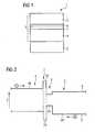
- FIG. 1 shows a schematic sectional view of a first exemplary embodiment of a radiation-emitting semiconductor chip according to the invention.
- the semiconductor chip 1 which is preferably designed as an LED chip, comprises a semiconductor body 3 arranged on a carrier 2.
- the semiconductor body has an n-conducting region 4 and a p-conducting region 5, between which an active region 6 suitable for the generation of radiation is arranged.
- the n-type and / or the p-type region may include a plurality of semiconductor layers (not shown).
- a hole barrier layer 7 Integrated between the n-type region 4 and the active region 6 or in the n-type region.
- the hole barrier layer 7 adjoins or limits the active region 6.
- the hole barrier layer 7 is based on a nitride compound semiconductor material from the material system In y Ga 1-xy Al x N with 0 ⁇ xs 1, 0 ⁇ y ⁇ 1 and x + ys 1 and is formed such that they penetrate holes, which in the operation of the semiconductor chip 1 via the p-type region. 5 into the active zone, reduces or blocks completely.
- the hole barrier layer 7 is designed to be permeable. Electron-hole pairs can recombine in the active region under radiation generation.
- the semiconductor body 3 is preferably grown epitaxially on an epitaxial substrate.
- the carrier 2 can emerge in particular from the epitaxial substrate on which a semiconductor layer sequence has grown for the semiconductor body.
- the semiconductor body is furthermore preferably based on nitride compound semiconductor materials.
- An SiC substrate or a sapphire substrate is particularly suitable here as an epitaxial substrate.
- the semiconductor chip is preferably designed for generating ultraviolet or visible radiation, in particular from the blue to the green spectral range.
- nitride compound semiconductors are particularly suitable.
- the active region 6 is expediently designed in such a way that both the electrons in the conduction band and the holes in the valence band are formed around the active region 6 on both sides of barriers which enclose charge carriers in the active region.
- the internal quantum efficiency of the semiconductor chip can thus be increased.
- one of these barriers is formed by the hole barrier layer, which accordingly may also be formed as an inclusion layer.
- the active region 6 comprises a single or multiple quantum well structure. Such structures are particularly suitable for forming an active region of high internal quantum efficiency.
- quantum well structure encompasses any structure in which charge carriers undergo quantization of their energy states by confinement.
- Name Quantum well structure No information about the dimensionality of the quantization. It thus includes quantum wells, quantum wires and quantum dots and any combination of these structures.
- a potential barrier is preferably formed for the holes, via which the penetration of holes into the n-conducting region is hindered.
- the probability of non-radiative recombination of electrons and holes outside the active region in the n-type region can thus be reduced.
- the internal quantum efficiency of the semiconductor chip can be stabilized even at high current densities.
- the likelihood of penetration of holes directed to the active region via the p-type region would increase to the n-type region 4. The internal quantum efficiency would then be reduced accordingly.
- the potential barrier to be overcome by holes for entry into the n-conducting region 4 is therefore preferably increased with respect to a semiconductor body without a hole barrier layer.
- the barrier height can be influenced by means of the band gap of the hole barrier layer 7 and / or by suitable doping of the hole barrier layer.
- the bandgap e.g. can be adjusted via the aluminum content x of the hole-barrier layer, with increasing aluminum content and the band gap increases.
- An aluminum content x of 0.2 or more is particularly suitable for a hole barrier layer 7.
- the indium content y of the hole Barrier layer 7 preferably greater than 0 selected. If the hole barrier layer 7 contains both indium and aluminum and optionally gallium, then y ⁇ x preferably applies.
- an indium content y which is lower than the aluminum content x, is particularly suitable, in particular for an active region based on In y Ga 1-y N.
- the hole barrier layer can simultaneously be embodied as a buffer layer for the active region 6 and as a barrier layer for holes.
- the aluminum content is preferred, in particular for an indium-free hole barrier layer, less than or equal to 0.45. Tensions can be kept so low.
- the hole barrier layer 7 is designed as a tunnel barrier layer.
- An example of a band diagram for a tunnel barrier layer is shown schematically in FIG. FIG. 2 schematically shows the profile of the conduction band edge 8 and the valence band edge 9 in the semiconductor body 3 of the semiconductor chip, which is preferably operated in the forward direction.
- the conduction band edge 78 of the formed as a tunnel barrier layer hole-barrier layer 7 is energetically above the conduction band edge 48 of the n-type region 4 adjacent to the hole-barrier layer 7 layer.
- the valence band edge 79 of the tunnel barrier layer lies energetically below the valence band edge 69 of the active region and preferably below the valence band edge 59 of the layer adjacent to the active region 6 on the side of the p-type region 5. Electrons coming from the n-type region 4 are guided to the active region 6, as well as holes for penetration into the n-type region must overcome a potential barrier.
- the height of the potential barrier to be overcome for electrons is given by the difference of the energies of the conduction band edge 78 and the conduction band edge 48, the height of the potential barrier for the holes by the difference of the energies of the valence band edge 69 and the valence band edge 79.
- the tunneling probability with which the charge carriers tunnel through the tunnel barrier layer depends on the respective barrier height to be overcome and the thickness of the tunnel barrier layer.
- the tunneling probability T is proportional to T ⁇ exp - 2 ⁇ d ⁇ ⁇ 2 ⁇ m ⁇ V 0 - e with the absolute barrier height V 0 , the barrier thickness d, as well as the energy E of the charge carriers and the effective mass m of the respective charge carriers.
- the barrier height to be overcome by the charge carriers is determined by the difference between the absolute barrier height V 0 -the energy of the conduction or valence band edge of the tunnel barrier layer-and the energy E of the respective charge carriers.
- the barrier height can be adjusted via the band gap, that is to say the difference between the energies of the valence band edge and the conduction band edge of the hole barrier layer 7. As already stated above, this can be done via the aluminum content x.
- FIG. 3 shows the dependence of the tunneling probability 10 for electrons and the tunneling probability 11 for holes as a function of the thickness d of the tunnel barrier layer in nanometers for an Al 0.5 Ga 0.5 N tunnel barrier layer in a diagram.
- Tunneling probabilities were determined based on the above relationship. Because the effective mass of Holes is larger than that of the electrons, the tunneling probability decreases 11 with increasing thickness of the tunnel barrier layer much more than that of the electrons. The effective mass of the holes is about ten times or more the effective mass of the electrons. This results in different tunneling probabilities for electrons and holes, so that charge-carrier asymmetric tunnels (Carrier Asymmetric Tunneling) electrons tunnel through the tunnel barrier layer to a much greater extent than holes. Holes are mostly held by the active region 6 by means of the tunnel barrier layer.
- the tunneling probability of the electrons through the tunnel barrier layer may be ten times or more, preferably one hundred times or more, more preferably a thousand times or more, the tunneling probability of the holes through the tunnel barrier layer. This can be achieved by suitable design of the tunnel barrier layer.
- the thickness of the tunnel barrier layer is 8 nm or less, more preferably 4 nm or less.
- a thickness of greater than or equal to 1 nm has been found to be particularly advantageous.
- x values are particularly suitable between in each case including 0.2 and 0.45, preferably greater than or equal to 0.3. Especially with regard to moderate lattice mismatch tunnel barrier layers with such aluminum content are particularly suitable.
- the tunnel barrier layer can be doped n-type, for example.
- the conduction band edge 78 of the tunnel barrier layer is then lowered, as is the valence band edge 79 of the tunnel barrier layer.
- the band gap remains essentially constant, so that the barrier height for holes is increased while the barrier height for electrons is reduced.
- a dopant with comparatively low donor levels, for example Si, is particularly suitable for this purpose.
- targeted impurities may be incorporated into the tunnel barrier layer that assist in tunneling the electrons to hole tunneling (trap assisted tunneling) and accordingly increase the tunneling probability for electrons relative to that of the holes.
- impurity atom for example, Si is suitable.
- a targeted reduction of the potential barrier for the electrons is indicated by dashed lines in FIG.
- the current density dependence of the internal quantum efficiency can advantageously be reduced since the holes, even at high current densities, increasingly recombine radiatively in the active region 6 and effectively block the penetration of holes into the n-conductive region by means of the tunnel barrier layer becomes.
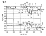
- FIG. 4 shows the influence of the aluminum content on the barrier height of an Al x Ga 1 -x N tunnel barrier layer with x> 0 on the basis of band diagrams determined in a simulation calculation.
- the W direction indicates the growth direction of the semiconductor body in which the individual layers for the semiconductor body, for example epitaxially on an epitaxial substrate, were grown successively.
- the conduction band edge 128 and the valence band edge 129 correspond to a nitride compound semiconductor-based semiconductor body without an aluminum-containing tunnel barrier layer.
- the semiconductor chip with the semiconductor body was assumed to be operated at 3.4 volts in the forward direction.
- the tunnel barrier layer 7b has an aluminum content of 0.3.
- the barrier height of the potential barrier of the tunnel barrier layer increases for electrons as well as for holes with the increasing band gap of the tunnel barrier layer due to the increasing aluminum content.
- the arrow 12 symbolizes a tunneling of the electrons into the active region.
- the hole-barrier layer 7 is designed as a pure hole-barrier layer.
- a pure hole barrier layer in contrast to a tunnel barrier layer, electrons pass from the n-type region 4 into the active region 6 substantially unhindered, that is to say without potential barriers.
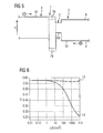
- FIG. 5 shows schematically a band diagram for a pure hole barrier layer.
- the hole barrier layer 7 has a conduction band edge 78 whose energy is less than or equal to that of the conduction band edge 48 of a layer adjoining the pure hole barrier layer 7 on the part of the n-type region 4.
- the valence band edge 79 of the pure hole barrier layer is lower in energy than the valence band edge 69 of the layer adjacent to the active region, and preferably lower in energy than the valence band edge 59 of a layer adjacent to the active region 6 on the part of the p-type region 5.
- the pure hole barrier layer can be made comparatively thick, since tunneling through of electrons does not have to be considered.
- the probability of penetration of holes into the n-type region can thus be kept extremely low, for example less than or equal to 10 -4 or less than or equal to 10 -5 .
- the pure hole barrier layer has an aluminum content between 0.2 and 0.3 inclusive.
- a thickness of the pure hole barrier layer may be between 11 nm and 30 nm inclusive.
- the pure hole barrier layer can also be made thicker.
- the pure hole-barrier layer is preferably more heavily doped (n + ) than a layer arranged on the side of the n-conductive region, in particular adjacent to the hole-barrier layer. Forming an electronically barrier-free transition to the active region can thus be facilitated.
- the conduction band edge 78 of the hole barrier layer may also lie below the conduction band edge 48 in terms of energy. This is indicated by dashed lines in FIG.
- FIG. 6 shows the dependence of the internal quantum efficiency Q in percent of the semiconductor chip 1 on the operating current density j in amperes per square centimeter.
- the current density j is plotted logarithmically.
- the curve 14 was for a semiconductor chip with a semiconductor body based on nitride compound semiconductor determined without aluminum-containing hole barrier layer and the curve 13 for a corresponding semiconductor body with aluminum-containing hole-barrier layer.
- the dependence of the internal quantum efficiency Q on the current density j is greatly reduced in the case of the curve 13 with respect to the curve 14.
- the internal quantum efficiency for the semiconductor chip with the hole barrier layer is substantially constant and independent of the operating current density.
- FIG. 7 shows a schematic sectional view of a second exemplary embodiment of a semiconductor chip 1 according to the invention.
- the semiconductor chip 1 corresponds to the semiconductor chip described in connection with FIG.
- the semiconductor chip 1 shown in FIG. 7 is designed as a thin-film chip.
- the carrier 2 is different from an epitaxial substrate on which a semiconductor layer sequence for the semiconductor body 3 has grown epitaxially.
- the semiconductor body 3 can be manufactured on the epitaxial substrate and subsequently arranged with its side facing away from the epitaxial substrate on the carrier 2 and preferably fixed.
- the carrier 2 does not have to meet the stringent requirements for an epitaxial substrate.
- the epitaxial substrate can be removed so that the thin-film chip is free of an epitaxial substrate. For example, etching, water jet cutting or a laser separation method is suitable for this purpose.
- nitride compound semiconductor-based semiconductor body for example, SiC or sapphire is suitable as a material for the epitaxial substrate.
- the carrier may also contain such materials.
- the carrier may be metallic or ceramic.
- a, in particular metallic, mirror layer 15 is arranged between the carrier 2 and the semiconductor body 3.
- This can prevent absorption in the active region 6 of generated radiation in a possibly absorbing carrier by reflection of the radiation at the mirror layer.
- the radiation component emerging from the semiconductor body 3 via the main surface 16 remote from the carrier can be increased due to the mirror layer.
- a connecting layer 17 is preferably arranged, by means of which the semiconductor body 3 is fixed on the carrier 2.
- the bonding layer 17 may be implemented, for example, as a solder layer or a layer formed in a wafer bonding process.
- the connection layer 17, the mirror layer 15 and / or the carrier 2 is designed to be electrically conductive.
- connection layer 17, the mirror layer 15 and / or the carrier 2 is electrically conductively connected to the active region 6.
- the active region 6 can thus be electrically contacted by means of a contact layer (not shown) arranged on the side of the carrier facing away from the semiconductor body.
- a corresponding mating contact layer (not shown) may be disposed on the main surface 16.
- This contact layer (s) is (are) preferably made metallic.
- the mirror layer 15 preferably contains Al, Ag, Pt or an alloy with at least one of these materials. These materials can advantageously have high reflectivities in the spectral ranges mentioned.
- the hole barrier layer 7 is in the case of the thin-film chip on the side of the active region 6 facing away from the carrier 2 arranged, since the semiconductor body after completion of the growth with the p-type region 5 has been arranged on the support 2.
- the hole barrier layer may be formed according to the above embodiments, wherein the efficiency, in particular the Auskoppeleffizienz, the semiconductor chip due to the mirror layer and the relatively free choice of the carrier may be advantageously increased.
- a hole barrier layer according to the invention can be applied not only to LED chips, but also to optical cavity laser chips such as an edge emitting laser chip, an internal cavity VCSEL, a Vertical External Cylinder Surface Emitting Laser (VECSEL). with external resonator or a RCLED (Resonant Cavity Light Emitting Diode) can be used.
- optical cavity laser chips such as an edge emitting laser chip, an internal cavity VCSEL, a Vertical External Cylinder Surface Emitting Laser (VECSEL). with external resonator or a RCLED (Resonant Cavity Light Emitting Diode) can be used.
Landscapes
- Led Devices (AREA)
- Semiconductor Lasers (AREA)
Applications Claiming Priority (2)
| Application Number | Priority Date | Filing Date | Title |
|---|---|---|---|
| DE102005035721 | 2005-07-29 | ||
| DE102005048196.5A DE102005048196B4 (de) | 2005-07-29 | 2005-10-07 | Strahlungsemittierender Halbleiterchip |
Publications (3)
| Publication Number | Publication Date |
|---|---|
| EP1748496A2 true EP1748496A2 (fr) | 2007-01-31 |
| EP1748496A3 EP1748496A3 (fr) | 2011-04-20 |
| EP1748496B1 EP1748496B1 (fr) | 2019-04-24 |
Family
ID=36790894
Family Applications (1)
| Application Number | Title | Priority Date | Filing Date |
|---|---|---|---|
| EP06014455.7A Active EP1748496B1 (fr) | 2005-07-29 | 2006-07-12 | Puce semi-conductrice électroluminescente |
Country Status (4)
| Country | Link |
|---|---|
| US (1) | US7791081B2 (fr) |
| EP (1) | EP1748496B1 (fr) |
| JP (1) | JP2007043151A (fr) |
| DE (1) | DE102005048196B4 (fr) |
Cited By (1)
| Publication number | Priority date | Publication date | Assignee | Title |
|---|---|---|---|---|
| WO2009006870A3 (fr) * | 2007-07-09 | 2009-06-18 | Osram Opto Semiconductors Gmbh | Corps semi-conducteur émetteur de rayonnement |
Families Citing this family (10)
| Publication number | Priority date | Publication date | Assignee | Title |
|---|---|---|---|---|
| EP1569263B1 (fr) * | 2004-02-27 | 2011-11-23 | OSRAM Opto Semiconductors GmbH | Procédé pour coller deux plaquettes |
| DE102007058952A1 (de) * | 2007-09-24 | 2009-04-09 | Osram Opto Semiconductors Gmbh | Optoelektronisches Bauelement |
| TWI557936B (zh) * | 2010-04-30 | 2016-11-11 | 美國波士頓大學信託會 | 具能帶結構位變動之高效率紫外光發光二極體 |
| US8379684B1 (en) * | 2011-08-16 | 2013-02-19 | Corning Incorporated | Hole blocking layers in non-polar and semi-polar green light emitting devices |
| JP5737096B2 (ja) * | 2011-09-13 | 2015-06-17 | 豊田合成株式会社 | Iii族窒化物半導体発光素子 |
| TW201347233A (zh) * | 2012-05-08 | 2013-11-16 | 華夏光股份有限公司 | 發光二極體裝置及其製造方法 |
| KR20220058643A (ko) | 2015-06-05 | 2022-05-09 | 오스텐도 테크놀로지스 인코포레이티드 | 다수의 활성층들로 선택적으로 캐리어를 주입한 발광 구조체 |
| JPWO2017119365A1 (ja) * | 2016-01-08 | 2018-11-01 | ソニー株式会社 | 半導体発光素子、表示装置および電子機器 |
| JP6399011B2 (ja) * | 2016-02-09 | 2018-10-03 | 日亜化学工業株式会社 | 光源装置 |
| DE102016109022B4 (de) * | 2016-05-17 | 2021-02-18 | OSRAM Opto Semiconductors Gesellschaft mit beschränkter Haftung | Laserdiodenchip |
Family Cites Families (20)
| Publication number | Priority date | Publication date | Assignee | Title |
|---|---|---|---|---|
| JPS63252492A (ja) * | 1987-04-09 | 1988-10-19 | Hikari Gijutsu Kenkyu Kaihatsu Kk | 半導体発光素子 |
| EP0575684A1 (fr) * | 1992-06-22 | 1993-12-29 | International Business Machines Corporation | Diode laser avec un confinement optique et électronique découplé |
| JPH06209139A (ja) * | 1993-01-11 | 1994-07-26 | Fujitsu Ltd | 半導体レーザ装置 |
| EP0772249B1 (fr) * | 1995-11-06 | 2006-05-03 | Nichia Corporation | Dispositif semi-conducteur comprenant un composé de nitrure |
| JP3658112B2 (ja) * | 1995-11-06 | 2005-06-08 | 日亜化学工業株式会社 | 窒化物半導体レーザダイオード |
| US5889295A (en) * | 1996-02-26 | 1999-03-30 | Kabushiki Kaisha Toshiba | Semiconductor device |
| JPH1056236A (ja) * | 1996-08-08 | 1998-02-24 | Toyoda Gosei Co Ltd | 3族窒化物半導体レーザ素子 |
| GB2327145A (en) * | 1997-07-10 | 1999-01-13 | Sharp Kk | Graded layers in an optoelectronic semiconductor device |
| TW412889B (en) * | 1997-09-24 | 2000-11-21 | Nippon Oxygen Co Ltd | Semiconductor laser |
| GB9912583D0 (en) * | 1999-05-28 | 1999-07-28 | Arima Optoelectronics Corp | A light emitting diode having a two well system with asymmetric tunneling |
| JP4161603B2 (ja) * | 2001-03-28 | 2008-10-08 | 日亜化学工業株式会社 | 窒化物半導体素子 |
| JP3645233B2 (ja) * | 2001-06-07 | 2005-05-11 | 日本電信電話株式会社 | 半導体素子 |
| JP3763754B2 (ja) * | 2001-06-07 | 2006-04-05 | 豊田合成株式会社 | Iii族窒化物系化合物半導体発光素子 |
| US7358522B2 (en) * | 2001-11-05 | 2008-04-15 | Nichia Corporation | Semiconductor device |
| TW567618B (en) * | 2002-07-15 | 2003-12-21 | Epistar Corp | Light emitting diode with adhesive reflection layer and manufacturing method thereof |
| CN100521260C (zh) * | 2002-07-16 | 2009-07-29 | 氮化物半导体株式会社 | 氮化镓类化合物半导体装置 |
| JP2004111514A (ja) * | 2002-09-17 | 2004-04-08 | Sanyo Electric Co Ltd | 窒化物系半導体発光素子およびその製造方法 |
| JP2007504682A (ja) * | 2003-05-09 | 2007-03-01 | クリー インコーポレイテッド | 高Al含量AlGaN拡散バリアを有するIII族窒化物電子素子構造 |
| GB2407701A (en) * | 2003-10-28 | 2005-05-04 | Sharp Kk | Manufacture of a semiconductor light-emitting device |
| KR100565894B1 (ko) * | 2005-07-06 | 2006-03-31 | (주)룩셀런트 | 3족 질화물 반도체 발광소자의 활성층을 제어하는 방법 |
-
2005
- 2005-10-07 DE DE102005048196.5A patent/DE102005048196B4/de not_active Expired - Lifetime
-
2006
- 2006-07-12 EP EP06014455.7A patent/EP1748496B1/fr active Active
- 2006-07-27 JP JP2006205165A patent/JP2007043151A/ja active Pending
- 2006-07-28 US US11/494,984 patent/US7791081B2/en active Active
Cited By (2)
| Publication number | Priority date | Publication date | Assignee | Title |
|---|---|---|---|---|
| WO2009006870A3 (fr) * | 2007-07-09 | 2009-06-18 | Osram Opto Semiconductors Gmbh | Corps semi-conducteur émetteur de rayonnement |
| US8314415B2 (en) | 2007-07-09 | 2012-11-20 | Osram Opto Semiconductors Gmbh | Radiation-emitting semiconductor body |
Also Published As
| Publication number | Publication date |
|---|---|
| US7791081B2 (en) | 2010-09-07 |
| EP1748496A3 (fr) | 2011-04-20 |
| DE102005048196A1 (de) | 2007-02-01 |
| DE102005048196B4 (de) | 2023-01-26 |
| EP1748496B1 (fr) | 2019-04-24 |
| US20100181583A1 (en) | 2010-07-22 |
| JP2007043151A (ja) | 2007-02-15 |
Similar Documents
| Publication | Publication Date | Title |
|---|---|---|
| EP2165374B1 (fr) | Corps semi-conducteur émetteur de rayonnement | |
| EP2212931B1 (fr) | Led comportant une couche de diffusion de courant | |
| EP2047527B1 (fr) | Corps semi-conducteur de del | |
| DE69636088T2 (de) | Halbleitervorrichtung aus einer Nitridverbindung | |
| DE102005035722B4 (de) | Optoelektronischer Halbleiterchip und Verfahren zu dessen Herstellung | |
| EP2208240B1 (fr) | Puce semi-conductrice optoélectronique à structure de puits quantiques multiples | |
| EP2519980B1 (fr) | Puce à semi-conducteurs électroluminescente | |
| EP1920469B1 (fr) | Procede pour separer lateralement une plaquette a semi-conducteurs et element optoelectronique | |
| EP1883140A1 (fr) | LD ou DEL avec une couche de revêtment superréseau et dopage gradué | |
| EP1883141A1 (fr) | LD ou DEL avec une couche de revêtement superréseau | |
| DE112018000553B4 (de) | Optoelektronischer Halbleiterchip | |
| WO2018050466A1 (fr) | Série de couches semi-conductrices | |
| EP1748496B1 (fr) | Puce semi-conductrice électroluminescente | |
| EP1883119B1 (fr) | Structure de recouvrement semi-conductrice dotée d'une surgrille | |
| DE102007057756B4 (de) | Verfahren zur Herstellung eines optoelektronischen Halbleiterkörpers | |
| DE102017122032A1 (de) | Laserdiode | |
| EP2465148B1 (fr) | Puce semi-conductrice optoélectronique pompée électriquement | |
| EP1873879B1 (fr) | Laser semi-conducteur à émission latérale | |
| DE102006046237A1 (de) | Halbleiter-Schichtstruktur mit Übergitter | |
| WO2014029633A1 (fr) | Corps semiconducteur optoélectronique et puce semiconductrice optoélectronique | |
| DE102012025904B4 (de) | Optoelektronischer Halbleiterkörper und optoelektronischer Halbleiterchip | |
| WO2023006577A1 (fr) | Corps semi-conducteur émetteur de rayonnement, diode laser et diode électroluminescente | |
| DE102006046228A1 (de) | Halbleiter-Schichtstruktur mit Übergitter |
Legal Events
| Date | Code | Title | Description |
|---|---|---|---|
| PUAI | Public reference made under article 153(3) epc to a published international application that has entered the european phase |
Free format text: ORIGINAL CODE: 0009012 |
|
| AK | Designated contracting states |
Kind code of ref document: A2 Designated state(s): AT BE BG CH CY CZ DE DK EE ES FI FR GB GR HU IE IS IT LI LT LU LV MC NL PL PT RO SE SI SK TR |
|
| AX | Request for extension of the european patent |
Extension state: AL BA HR MK YU |
|
| RAP1 | Party data changed (applicant data changed or rights of an application transferred) |
Owner name: OSRAM OPTO SEMICONDUCTORS GMBH |
|
| RAP1 | Party data changed (applicant data changed or rights of an application transferred) |
Owner name: OSRAM OPTO SEMICONDUCTORS GMBH |
|
| PUAL | Search report despatched |
Free format text: ORIGINAL CODE: 0009013 |
|
| REG | Reference to a national code |
Ref country code: DE Ref legal event code: R079 Free format text: PREVIOUS MAIN CLASS: H01L0033000000 Ipc: H01L0033040000 |
|
| AK | Designated contracting states |
Kind code of ref document: A3 Designated state(s): AT BE BG CH CY CZ DE DK EE ES FI FR GB GR HU IE IS IT LI LT LU LV MC NL PL PT RO SE SI SK TR |
|
| AX | Request for extension of the european patent |
Extension state: AL BA HR MK RS |
|
| RIC1 | Information provided on ipc code assigned before grant |
Ipc: H01L 33/04 20100101AFI20110311BHEP |
|
| 17P | Request for examination filed |
Effective date: 20111020 |
|
| AKX | Designation fees paid |
Designated state(s): AT BE BG CH CY CZ DE DK EE ES FI FR GB GR HU IE IS IT LI LT LU LV MC NL PL PT RO SE SI SK TR |
|
| 17Q | First examination report despatched |
Effective date: 20160115 |
|
| RIC1 | Information provided on ipc code assigned before grant |
Ipc: H01L 33/14 20100101AFI20180425BHEP Ipc: H01L 33/12 20100101ALI20180425BHEP Ipc: H01L 33/32 20100101ALN20180425BHEP Ipc: H01L 33/04 20100101ALI20180425BHEP Ipc: H01L 33/02 20100101ALN20180425BHEP Ipc: H01S 5/323 20060101ALN20180425BHEP |
|
| GRAP | Despatch of communication of intention to grant a patent |
Free format text: ORIGINAL CODE: EPIDOSNIGR1 |
|
| STAA | Information on the status of an ep patent application or granted ep patent |
Free format text: STATUS: GRANT OF PATENT IS INTENDED |
|
| INTG | Intention to grant announced |
Effective date: 20180628 |
|
| RIN1 | Information on inventor provided before grant (corrected) |
Inventor name: PETER, MATTHIAS Inventor name: STRAUSS, UWE Inventor name: SABATHIL, MATTHIAS |
|
| GRAJ | Information related to disapproval of communication of intention to grant by the applicant or resumption of examination proceedings by the epo deleted |
Free format text: ORIGINAL CODE: EPIDOSDIGR1 |
|
| STAA | Information on the status of an ep patent application or granted ep patent |
Free format text: STATUS: EXAMINATION IS IN PROGRESS |
|
| REG | Reference to a national code |
Ref country code: DE Ref legal event code: R079 Ref document number: 502006016234 Country of ref document: DE Free format text: PREVIOUS MAIN CLASS: H01L0033040000 Ipc: H01L0033140000 |
|
| INTC | Intention to grant announced (deleted) | ||
| RIC1 | Information provided on ipc code assigned before grant |
Ipc: H01L 33/12 20070131ALI20181108BHEP Ipc: H01L 33/32 20070131ALN20181108BHEP Ipc: H01S 5/323 20060101ALN20181108BHEP Ipc: H01L 33/02 20070131ALN20181108BHEP Ipc: H01L 33/04 20070131ALI20181108BHEP Ipc: H01L 33/14 20070131AFI20181108BHEP |
|
| GRAP | Despatch of communication of intention to grant a patent |
Free format text: ORIGINAL CODE: EPIDOSNIGR1 |
|
| RIC1 | Information provided on ipc code assigned before grant |
Ipc: H01L 33/32 20100101ALN20181108BHEP Ipc: H01L 33/14 20100101AFI20181108BHEP Ipc: H01S 5/323 20060101ALN20181108BHEP Ipc: H01L 33/02 20100101ALN20181108BHEP Ipc: H01L 33/04 20100101ALI20181108BHEP Ipc: H01L 33/12 20100101ALI20181108BHEP |
|
| STAA | Information on the status of an ep patent application or granted ep patent |
Free format text: STATUS: GRANT OF PATENT IS INTENDED |
|
| INTG | Intention to grant announced |
Effective date: 20190103 |
|
| RIC1 | Information provided on ipc code assigned before grant |
Ipc: H01L 33/12 20100101ALI20181108BHEP Ipc: H01S 5/323 20060101ALN20181108BHEP Ipc: H01L 33/14 20100101AFI20181108BHEP Ipc: H01L 33/02 20100101ALN20181108BHEP Ipc: H01L 33/04 20100101ALI20181108BHEP Ipc: H01L 33/32 20100101ALN20181108BHEP |
|
| GRAS | Grant fee paid |
Free format text: ORIGINAL CODE: EPIDOSNIGR3 |
|
| GRAA | (expected) grant |
Free format text: ORIGINAL CODE: 0009210 |
|
| STAA | Information on the status of an ep patent application or granted ep patent |
Free format text: STATUS: THE PATENT HAS BEEN GRANTED |
|
| AK | Designated contracting states |
Kind code of ref document: B1 Designated state(s): AT BE BG CH CY CZ DE DK EE ES FI FR GB GR HU IE IS IT LI LT LU LV MC NL PL PT RO SE SI SK TR |
|
| REG | Reference to a national code |
Ref country code: GB Ref legal event code: FG4D Free format text: NOT ENGLISH |
|
| REG | Reference to a national code |
Ref country code: CH Ref legal event code: EP |
|
| REG | Reference to a national code |
Ref country code: AT Ref legal event code: REF Ref document number: 1125171 Country of ref document: AT Kind code of ref document: T Effective date: 20190515 Ref country code: IE Ref legal event code: FG4D Free format text: LANGUAGE OF EP DOCUMENT: GERMAN |
|
| REG | Reference to a national code |
Ref country code: DE Ref legal event code: R096 Ref document number: 502006016234 Country of ref document: DE |
|
| REG | Reference to a national code |
Ref country code: NL Ref legal event code: MP Effective date: 20190424 |
|
| REG | Reference to a national code |
Ref country code: LT Ref legal event code: MG4D |
|
| RAP2 | Party data changed (patent owner data changed or rights of a patent transferred) |
Owner name: OSRAM OPTO SEMICONDUCTORS GMBH |
|
| PG25 | Lapsed in a contracting state [announced via postgrant information from national office to epo] |
Ref country code: NL Free format text: LAPSE BECAUSE OF FAILURE TO SUBMIT A TRANSLATION OF THE DESCRIPTION OR TO PAY THE FEE WITHIN THE PRESCRIBED TIME-LIMIT Effective date: 20190424 |
|
| PG25 | Lapsed in a contracting state [announced via postgrant information from national office to epo] |
Ref country code: SE Free format text: LAPSE BECAUSE OF FAILURE TO SUBMIT A TRANSLATION OF THE DESCRIPTION OR TO PAY THE FEE WITHIN THE PRESCRIBED TIME-LIMIT Effective date: 20190424 Ref country code: ES Free format text: LAPSE BECAUSE OF FAILURE TO SUBMIT A TRANSLATION OF THE DESCRIPTION OR TO PAY THE FEE WITHIN THE PRESCRIBED TIME-LIMIT Effective date: 20190424 Ref country code: PT Free format text: LAPSE BECAUSE OF FAILURE TO SUBMIT A TRANSLATION OF THE DESCRIPTION OR TO PAY THE FEE WITHIN THE PRESCRIBED TIME-LIMIT Effective date: 20190824 Ref country code: FI Free format text: LAPSE BECAUSE OF FAILURE TO SUBMIT A TRANSLATION OF THE DESCRIPTION OR TO PAY THE FEE WITHIN THE PRESCRIBED TIME-LIMIT Effective date: 20190424 Ref country code: LT Free format text: LAPSE BECAUSE OF FAILURE TO SUBMIT A TRANSLATION OF THE DESCRIPTION OR TO PAY THE FEE WITHIN THE PRESCRIBED TIME-LIMIT Effective date: 20190424 |
|
| PG25 | Lapsed in a contracting state [announced via postgrant information from national office to epo] |
Ref country code: PL Free format text: LAPSE BECAUSE OF FAILURE TO SUBMIT A TRANSLATION OF THE DESCRIPTION OR TO PAY THE FEE WITHIN THE PRESCRIBED TIME-LIMIT Effective date: 20190424 Ref country code: GR Free format text: LAPSE BECAUSE OF FAILURE TO SUBMIT A TRANSLATION OF THE DESCRIPTION OR TO PAY THE FEE WITHIN THE PRESCRIBED TIME-LIMIT Effective date: 20190725 Ref country code: LV Free format text: LAPSE BECAUSE OF FAILURE TO SUBMIT A TRANSLATION OF THE DESCRIPTION OR TO PAY THE FEE WITHIN THE PRESCRIBED TIME-LIMIT Effective date: 20190424 Ref country code: BG Free format text: LAPSE BECAUSE OF FAILURE TO SUBMIT A TRANSLATION OF THE DESCRIPTION OR TO PAY THE FEE WITHIN THE PRESCRIBED TIME-LIMIT Effective date: 20190724 |
|
| PG25 | Lapsed in a contracting state [announced via postgrant information from national office to epo] |
Ref country code: IS Free format text: LAPSE BECAUSE OF FAILURE TO SUBMIT A TRANSLATION OF THE DESCRIPTION OR TO PAY THE FEE WITHIN THE PRESCRIBED TIME-LIMIT Effective date: 20190824 |
|
| REG | Reference to a national code |
Ref country code: DE Ref legal event code: R097 Ref document number: 502006016234 Country of ref document: DE |
|
| PG25 | Lapsed in a contracting state [announced via postgrant information from national office to epo] |
Ref country code: DK Free format text: LAPSE BECAUSE OF FAILURE TO SUBMIT A TRANSLATION OF THE DESCRIPTION OR TO PAY THE FEE WITHIN THE PRESCRIBED TIME-LIMIT Effective date: 20190424 Ref country code: EE Free format text: LAPSE BECAUSE OF FAILURE TO SUBMIT A TRANSLATION OF THE DESCRIPTION OR TO PAY THE FEE WITHIN THE PRESCRIBED TIME-LIMIT Effective date: 20190424 Ref country code: RO Free format text: LAPSE BECAUSE OF FAILURE TO SUBMIT A TRANSLATION OF THE DESCRIPTION OR TO PAY THE FEE WITHIN THE PRESCRIBED TIME-LIMIT Effective date: 20190424 Ref country code: SK Free format text: LAPSE BECAUSE OF FAILURE TO SUBMIT A TRANSLATION OF THE DESCRIPTION OR TO PAY THE FEE WITHIN THE PRESCRIBED TIME-LIMIT Effective date: 20190424 Ref country code: CZ Free format text: LAPSE BECAUSE OF FAILURE TO SUBMIT A TRANSLATION OF THE DESCRIPTION OR TO PAY THE FEE WITHIN THE PRESCRIBED TIME-LIMIT Effective date: 20190424 |
|
| PG25 | Lapsed in a contracting state [announced via postgrant information from national office to epo] |
Ref country code: MC Free format text: LAPSE BECAUSE OF FAILURE TO SUBMIT A TRANSLATION OF THE DESCRIPTION OR TO PAY THE FEE WITHIN THE PRESCRIBED TIME-LIMIT Effective date: 20190424 Ref country code: IT Free format text: LAPSE BECAUSE OF FAILURE TO SUBMIT A TRANSLATION OF THE DESCRIPTION OR TO PAY THE FEE WITHIN THE PRESCRIBED TIME-LIMIT Effective date: 20190424 |
|
| PLBE | No opposition filed within time limit |
Free format text: ORIGINAL CODE: 0009261 |
|
| REG | Reference to a national code |
Ref country code: CH Ref legal event code: PL |
|
| STAA | Information on the status of an ep patent application or granted ep patent |
Free format text: STATUS: NO OPPOSITION FILED WITHIN TIME LIMIT |
|
| GBPC | Gb: european patent ceased through non-payment of renewal fee |
Effective date: 20190724 |
|
| PG25 | Lapsed in a contracting state [announced via postgrant information from national office to epo] |
Ref country code: TR Free format text: LAPSE BECAUSE OF FAILURE TO SUBMIT A TRANSLATION OF THE DESCRIPTION OR TO PAY THE FEE WITHIN THE PRESCRIBED TIME-LIMIT Effective date: 20190424 |
|
| 26N | No opposition filed |
Effective date: 20200127 |
|
| REG | Reference to a national code |
Ref country code: BE Ref legal event code: MM Effective date: 20190731 |
|
| PG25 | Lapsed in a contracting state [announced via postgrant information from national office to epo] |
Ref country code: GB Free format text: LAPSE BECAUSE OF NON-PAYMENT OF DUE FEES Effective date: 20190724 |
|
| PG25 | Lapsed in a contracting state [announced via postgrant information from national office to epo] |
Ref country code: BE Free format text: LAPSE BECAUSE OF NON-PAYMENT OF DUE FEES Effective date: 20190731 Ref country code: LU Free format text: LAPSE BECAUSE OF NON-PAYMENT OF DUE FEES Effective date: 20190712 Ref country code: SI Free format text: LAPSE BECAUSE OF FAILURE TO SUBMIT A TRANSLATION OF THE DESCRIPTION OR TO PAY THE FEE WITHIN THE PRESCRIBED TIME-LIMIT Effective date: 20190424 Ref country code: CH Free format text: LAPSE BECAUSE OF NON-PAYMENT OF DUE FEES Effective date: 20190731 Ref country code: LI Free format text: LAPSE BECAUSE OF NON-PAYMENT OF DUE FEES Effective date: 20190731 |
|
| PG25 | Lapsed in a contracting state [announced via postgrant information from national office to epo] |
Ref country code: FR Free format text: LAPSE BECAUSE OF NON-PAYMENT OF DUE FEES Effective date: 20190731 |
|
| PG25 | Lapsed in a contracting state [announced via postgrant information from national office to epo] |
Ref country code: IE Free format text: LAPSE BECAUSE OF NON-PAYMENT OF DUE FEES Effective date: 20190712 |
|
| REG | Reference to a national code |
Ref country code: AT Ref legal event code: MM01 Ref document number: 1125171 Country of ref document: AT Kind code of ref document: T Effective date: 20190712 |
|
| PG25 | Lapsed in a contracting state [announced via postgrant information from national office to epo] |
Ref country code: AT Free format text: LAPSE BECAUSE OF NON-PAYMENT OF DUE FEES Effective date: 20190712 |
|
| PG25 | Lapsed in a contracting state [announced via postgrant information from national office to epo] |
Ref country code: CY Free format text: LAPSE BECAUSE OF FAILURE TO SUBMIT A TRANSLATION OF THE DESCRIPTION OR TO PAY THE FEE WITHIN THE PRESCRIBED TIME-LIMIT Effective date: 20190424 |
|
| PG25 | Lapsed in a contracting state [announced via postgrant information from national office to epo] |
Ref country code: HU Free format text: LAPSE BECAUSE OF FAILURE TO SUBMIT A TRANSLATION OF THE DESCRIPTION OR TO PAY THE FEE WITHIN THE PRESCRIBED TIME-LIMIT; INVALID AB INITIO Effective date: 20060712 |
|
| P01 | Opt-out of the competence of the unified patent court (upc) registered |
Effective date: 20230825 |
|
| REG | Reference to a national code |
Ref country code: DE Ref legal event code: R079 Ref document number: 502006016234 Country of ref document: DE Free format text: PREVIOUS MAIN CLASS: H01L0033140000 Ipc: H10H0020816000 |
|
| PGFP | Annual fee paid to national office [announced via postgrant information from national office to epo] |
Ref country code: DE Payment date: 20250722 Year of fee payment: 20 |