EP1748504A2 - Dispositif organique électroluminescent et sa méthode de fabrication - Google Patents
Dispositif organique électroluminescent et sa méthode de fabrication Download PDFInfo
- Publication number
- EP1748504A2 EP1748504A2 EP06003603A EP06003603A EP1748504A2 EP 1748504 A2 EP1748504 A2 EP 1748504A2 EP 06003603 A EP06003603 A EP 06003603A EP 06003603 A EP06003603 A EP 06003603A EP 1748504 A2 EP1748504 A2 EP 1748504A2
- Authority
- EP
- European Patent Office
- Prior art keywords
- electron
- transport layer
- properties
- electrode
- metal
- Prior art date
- Legal status (The legal status is an assumption and is not a legal conclusion. Google has not performed a legal analysis and makes no representation as to the accuracy of the status listed.)
- Granted
Links
Images










Classifications
-
- C—CHEMISTRY; METALLURGY
- C09—DYES; PAINTS; POLISHES; NATURAL RESINS; ADHESIVES; COMPOSITIONS NOT OTHERWISE PROVIDED FOR; APPLICATIONS OF MATERIALS NOT OTHERWISE PROVIDED FOR
- C09K—MATERIALS FOR MISCELLANEOUS APPLICATIONS, NOT PROVIDED FOR ELSEWHERE
- C09K11/00—Luminescent materials, e.g. electroluminescent or chemiluminescent
- C09K11/06—Luminescent materials, e.g. electroluminescent or chemiluminescent containing organic luminescent materials
-
- H—ELECTRICITY
- H10—SEMICONDUCTOR DEVICES; ELECTRIC SOLID-STATE DEVICES NOT OTHERWISE PROVIDED FOR
- H10K—ORGANIC ELECTRIC SOLID-STATE DEVICES
- H10K50/00—Organic light-emitting devices
- H10K50/10—OLEDs or polymer light-emitting diodes [PLED]
- H10K50/14—Carrier transporting layers
- H10K50/16—Electron transporting layers
-
- H—ELECTRICITY
- H05—ELECTRIC TECHNIQUES NOT OTHERWISE PROVIDED FOR
- H05B—ELECTRIC HEATING; ELECTRIC LIGHT SOURCES NOT OTHERWISE PROVIDED FOR; CIRCUIT ARRANGEMENTS FOR ELECTRIC LIGHT SOURCES, IN GENERAL
- H05B33/00—Electroluminescent light sources
- H05B33/12—Light sources with substantially two-dimensional [2D] radiating surfaces
- H05B33/26—Light sources with substantially two-dimensional [2D] radiating surfaces characterised by the composition or arrangement of the conductive material used as an electrode
-
- H—ELECTRICITY
- H10—SEMICONDUCTOR DEVICES; ELECTRIC SOLID-STATE DEVICES NOT OTHERWISE PROVIDED FOR
- H10K—ORGANIC ELECTRIC SOLID-STATE DEVICES
- H10K50/00—Organic light-emitting devices
- H10K50/10—OLEDs or polymer light-emitting diodes [PLED]
- H10K50/18—Carrier blocking layers
-
- H—ELECTRICITY
- H10—SEMICONDUCTOR DEVICES; ELECTRIC SOLID-STATE DEVICES NOT OTHERWISE PROVIDED FOR
- H10K—ORGANIC ELECTRIC SOLID-STATE DEVICES
- H10K2101/00—Properties of the organic materials covered by group H10K85/00
- H10K2101/10—Triplet emission
-
- H—ELECTRICITY
- H10—SEMICONDUCTOR DEVICES; ELECTRIC SOLID-STATE DEVICES NOT OTHERWISE PROVIDED FOR
- H10K—ORGANIC ELECTRIC SOLID-STATE DEVICES
- H10K50/00—Organic light-emitting devices
- H10K50/10—OLEDs or polymer light-emitting diodes [PLED]
- H10K50/11—OLEDs or polymer light-emitting diodes [PLED] characterised by the electroluminescent [EL] layers
-
- H—ELECTRICITY
- H10—SEMICONDUCTOR DEVICES; ELECTRIC SOLID-STATE DEVICES NOT OTHERWISE PROVIDED FOR
- H10K—ORGANIC ELECTRIC SOLID-STATE DEVICES
- H10K50/00—Organic light-emitting devices
- H10K50/10—OLEDs or polymer light-emitting diodes [PLED]
- H10K50/19—Tandem OLEDs
-
- H—ELECTRICITY
- H10—SEMICONDUCTOR DEVICES; ELECTRIC SOLID-STATE DEVICES NOT OTHERWISE PROVIDED FOR
- H10K—ORGANIC ELECTRIC SOLID-STATE DEVICES
- H10K59/00—Integrated devices, or assemblies of multiple devices, comprising at least one organic light-emitting element covered by group H10K50/00
- H10K59/30—Devices specially adapted for multicolour light emission
- H10K59/35—Devices specially adapted for multicolour light emission comprising red-green-blue [RGB] subpixels
-
- H—ELECTRICITY
- H10—SEMICONDUCTOR DEVICES; ELECTRIC SOLID-STATE DEVICES NOT OTHERWISE PROVIDED FOR
- H10K—ORGANIC ELECTRIC SOLID-STATE DEVICES
- H10K85/00—Organic materials used in the body or electrodes of devices covered by this subclass
- H10K85/30—Coordination compounds
- H10K85/321—Metal complexes comprising a group IIIA element, e.g. Tris (8-hydroxyquinoline) gallium [Gaq3]
- H10K85/324—Metal complexes comprising a group IIIA element, e.g. Tris (8-hydroxyquinoline) gallium [Gaq3] comprising aluminium, e.g. Alq3
-
- H—ELECTRICITY
- H10—SEMICONDUCTOR DEVICES; ELECTRIC SOLID-STATE DEVICES NOT OTHERWISE PROVIDED FOR
- H10K—ORGANIC ELECTRIC SOLID-STATE DEVICES
- H10K85/00—Organic materials used in the body or electrodes of devices covered by this subclass
- H10K85/30—Coordination compounds
- H10K85/341—Transition metal complexes, e.g. Ru(II)polypyridine complexes
- H10K85/342—Transition metal complexes, e.g. Ru(II)polypyridine complexes comprising iridium
-
- H—ELECTRICITY
- H10—SEMICONDUCTOR DEVICES; ELECTRIC SOLID-STATE DEVICES NOT OTHERWISE PROVIDED FOR
- H10K—ORGANIC ELECTRIC SOLID-STATE DEVICES
- H10K85/00—Organic materials used in the body or electrodes of devices covered by this subclass
- H10K85/60—Organic compounds having low molecular weight
-
- H—ELECTRICITY
- H10—SEMICONDUCTOR DEVICES; ELECTRIC SOLID-STATE DEVICES NOT OTHERWISE PROVIDED FOR
- H10K—ORGANIC ELECTRIC SOLID-STATE DEVICES
- H10K85/00—Organic materials used in the body or electrodes of devices covered by this subclass
- H10K85/60—Organic compounds having low molecular weight
- H10K85/649—Aromatic compounds comprising a hetero atom
Definitions
- the present invention relates to an organic electroluminescent (EL) device, and more particularly, to an organic electroluminescent device having an electron-transport layer and a method for fabricating the same.
- EL organic electroluminescent
- an organic electroluminescent (EL) device includes a stack of organic layers, each layer having a function related to an anode made of materials such as indium tin oxide (ITO) and a cathode made of materials such as aluminum (Al). An electric field is applied to the stack to emit light.
- Organic EL devices are characterized by the capability to be driven at a low voltage with relatively low consumption of electric power, while having a light-weight and flexible substrate.
- An object of the invention is to solve at least the above problems and/or disadvantages and to provide at least the advantages described hereinafter.
- the present invention is directed to an organic electroluminescent device and a method for fabricating the same that substantially obviate one or more problems due to limitations and disadvantages of the related art.
- An object of the present invention is to provide an organic electroluminescent device having an improved service life and efficiency via formation of an electron-transport layer utilizing a novel material, and a method for fabricating the same.
- Another object of the present invention is to provide an organic electroluminescent device involving a simplified manufacturing process via formation of an electron-transport layer utilizing a novel material, and a method for fabricating the same.
- an organic electroluminescent device includes a stack structure including an emitting layer and an electron-transport layer between an anode and a cathode, wherein the electron-transport layer is a mixture of at least two materials, and the mixture of at least two materials may be a mixture of an organic compound and one or more other organic compounds, or may be a mixture of a metal or inorganic compound and one or more other metal or inorganic compounds, or may be a mixture of one or more organic compounds and one or more metal or inorganic compounds.
- the electron-transport layer may be a mixture of a first material and a second material, and a composition ratio of the first material (X) to the second material (Y) may be in the range of 1 - 100:1 and 1:1 - 100.
- the electron-transport layer may be a mixture of a first material and plural materials, and a composition ratio of the first material (X) to the plural materials (Y) may be in the range of 1 - 100:1 and 1:1 - 100.
- the electron-transport layer may contain at least one material having hole-blocking properties and at least one material having electron-transporting properties.
- the material having hole-blocking properties may have an oxidation potential greater than 0.4V, and an absolute value of the Highest Occupied Molecular Orbital (HOMO) greater than 5.2 eV.
- HOMO Highest Occupied Molecular Orbital
- the material having electron-transporting properties may have a mobility of more than 1.0x10 -6 cm 2 /Vs.
- the electron-transport layer may contain at least one material having hole-blocking properties, at least one material having electron-transporting properties and at least one material having electron injection- or electron-transport-facilitating properties.
- a full-color organic electroluminescent (EL) device may include a stack structure including an emitting layer and an electron-transport layer between an anode and a cathode, wherein the emitting layer contains at least one phosphorescent material, and wherein the electron-transport layer may be a mixture of at least one material having hole-blocking properties and at least one material having electron-transporting properties.
- an organic electroluminescent device may include a multiplicity of light-emitting units including an emitting layer and an electron-transport layer between an anode and a cathode, wherein the adjacent emitting units are separated by interlayers, and wherein the electron-transport layer may be a mixture of at least one material having hole-blocking properties and at least one material having electron-transporting properties.
- the light-emitting units may be made up of the same stack structures or different stack structures.
- a method for fabricating an organic electroluminescent device includes forming a first electrode on a substrate, forming an emitting layer containing at least one phosphorescent material on the first electrode, forming, over the entire emitting layer, an electron-transport layer including a mixture of at least one material having hole-blocking properties and at least one material having electron-transporting properties, and forming a second electrode on the electron-transport layer.
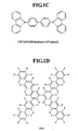
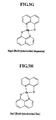
- FIGs. 1a to 1e are structural formulae of hole-blocking materials used in an electron-transport layer of an organic EL device in accordance with an embodiment of the invention
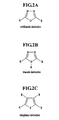
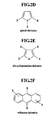
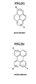
- FIGs. 2a to 2h are structural formulae of derivatives used in an electron-transport layer of an organic EL device in accordance with an embodiment of the invention
- FIGs. 3a to 3h are structural formulae of electron-transporting materials used in an electron-transport layer of an organic EL device in accordance with an embodiment of the invention
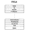
- FIGs. 4 to 7 are sectional views of organic EL devices in accordance with embodiments of the invention.
- FIGs. 8 and 9 are graphs comparing IVL characteristics with respect to materials used in an electron-transport layer
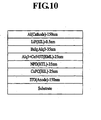
- FIG. 10 is a sectional view of an organic EL device having a Balq:Alq 3 electron-transport layer
- FIGs. 11 and 12 are graphs comparing characteristics of IVL with respect to a composition ratio of a Balq:Alq 3 electron-transport layer
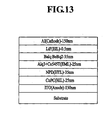
- FIG. 13 is a sectional view of an organic EL device having a Balq:BeBq 2 electron-transport layer
- FIG. 14 is a graph comparing service lives of devices with respect to materials used in an electron-transport layer.
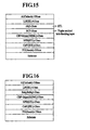
- FIGs. 15 and 16 are sectional views of an organic EL device illustrating characteristics of the invention.
- An organic electroluminescent (EL) device generates light of a certain wavelength via formation of excitons resulting from recombination between electrons and holes, injected via a cathode and an anode, in an emitting layer.
- EL organic electroluminescent
- An Internal Quantum Efficiency of the organic EL device is expressed by the ratio of the number of photons generated inside the device to the number of charges injected from the external electrode.
- a ground state of most molecules is a spin singlet state.
- singlet excitons are allowed for radiative transition to the ground state, which is called fluorescence. Radiative transition of triplet excitons, emitting light, into a singlet-ground state is preferably prohibited. Triplet excitons may also undergo transition through light emission by perturbation such as spin-orbit coupling, which is called phosphorescence.
- the balance between electron and hole injection is preferably maintained in order to obtain maximum efficiency thereof.
- This balance factor, y is referred to as a charge balance factor.
- An organic EL device in accordance with an embodiment of the invention primarily comprises a substrate, a first electrode formed on the substrate, an emitting layer formed on the first electrode, a second electrode formed on the emitting layer, and an electron-transport layer formed on at least one region, i.e., between the first electrode and emitting layer and between the second electrode and emitting layer.
- Any one of the first electrode and second electrode may be an anode or cathode formed of a transparent material.
- the electron-transport layer may include a mixture of at least two materials, and the mixture may be a mixture of at least two materials selected from an organic compound, a metal compound and an inorganic compound. More specifically, the electron-transport layer may be a mixture of an organic compound and one or more other organic compounds, or may be a mixture of a metal or inorganic compound and one or more other metal or inorganic compounds, or may be a mixture of one or more organic compounds and one or more metal or inorganic compounds.
- the electron-transport layer has a thickness of between approximately 0.1 and 500 nm.
- the electron-transport layer may be a mixture of a first material and a second material, wherein a composition ratio of the first material (X) and the second material (Y) is in the range of 1 - 100:1 and 1:1 - 100. Additionally, when the electron-transport layer is instead a mixture of a first material and plural materials, a composition ratio of the first material (X) to the plural materials (Z) may be in the range of between approximately 1 - 100:1 and 1:1 - 100.
- electron-transport layer includes at least one material having hole-blocking properties and at least one material having electron-transporting properties.
- the material having hole-blocking properties preferably has an oxidation potential greater than approximately 0.4V, and an absolute value of the Highest Occupied Molecular Orbital (HOMO) greater than approximately 5.2 eV.
- HOMO Highest Occupied Molecular Orbital
- a material having the absolute value of the HOMO of more than about 5.2 eV is preferably utilized as the hole-blocking material and serves to block holes and excitons formed in the emitting layer.
- the hole-blocking material may be a metal complex containing materials such as, for example, a substituted or unsubstituted 8-hydroxyquinoline, and the metal may be selected from metals such as, for example, aluminum (Al), zinc (Zn), magnesium (Mg) and lithium (Li). Other materials may also be appropriate.
- the hole-blocking material may be a substituted or unsubstituted 1,10-phenanthroline derivative, or may be a substituted or unsubstituted carbazole derivative.
- the hole-blocking material may be selected from materials such as, for example, Balq (aluminum(III) bis(2-methyl-8-quinolinato) 4-phenylphenolate), BCP (2,9-dimethyl-4,7-diphenyl-1,10-phenanthroline), CBP [4,48-N,N8-dicarbazole-1,18-biphenyl], CF-X and CF-Y. Other materials may also be appropriate.
- the material having electron-transporting properties has a mobility of more than approximately 1.0x10 -6 cm 2 /Vs. Other levels of mobility may also be appropriate, based on the material selected.
- the material having electron-transporting properties may be selected from materials such as, for example, a substituted or unsubstituted aluminum (Al) complex, a substituted or unsubstituted beryllium (Be) complex, a substituted or unsubstituted zinc (Zn) complex, a substituted or unsubstituted oxidiazole derivative, a substituted or unsubstituted triazole derivative, a substituted or unsubstituted thiophene derivative, a substituted or unsubstituted pyrrole derivative, a substituted or unsubstituted sila-cyclopentadiene derivative, a substituted or unsubstituted anthracene derivative, a substituted or unsubstituted pyrene derivative and a substituted or unsubstituted perylene derivative.
- materials such as, for example, a substituted or unsubstituted aluminum (Al) complex, a substituted or unsubstitute
- the material having electron-transporting properties may be selected from materials such as, for example, Alq 3 [Tris-(8-hydroxyquinolinolato)-aluminum], BeBq 2 [Bis(10-hydroxybenzo[h]quinolinato)beryllium], Zn(oxz) 2 [Bis(2-(2-hydroxyphenyl)-benz-1,3-oxadiazolato)zinc], PBD [2-(4-biphenylyl)-5-(4-tert-butyl-phenyl)-1,3,4-oxadiazole], TAZ [3-(4-biphenylyl)-4-phenyl-5-tert-butylphenyl-1,2,4-triazole], Liq [8-quinolinolato lithium], Mgq 2 [Bis(8-quinolinolato) magnesium] and Znq 2 [Bis(8-quinolinolato)zinc].
- materials such as, for example, Alq 3 [Tris-
- the electron-transport layer in accordance with the present invention may include at least one organic compound or at least one organic metal compound
- the organic compound or organic metal compound may be a phthalocyanine derivative and a metallophthalocyanine derivative, wherein a metal component may include any one of Co, AlCl, Cu, Li 2 , Fe, Pb, Mg, Na 2 , Sn, Zn, Ni, Mn, VO, Ag 2 , MnCl, SiCl 2 and SnCl 2
- the organic compound or organic metal compound may be a porphyrin derivative and a metalloporphyrin derivative, wherein a metal component may include any one of Co, AlCl, Cu, Li 2 , Fe, Pb, Mg, Na 2 , Sn, Zn, Ni, Mn, VO, Ag 2 , MnCl, SiCl 2 and SnCl 2 .
- the electron-transport layer may include at least one material having hole-blocking properties, at least one material having electron-transporting properties, and at least one material having electron-injection-facilitating properties or electron-transport-facilitating properties.
- the material having electron-injection-facilitating properties or electron-transport-facilitating properties may be an inorganic compound or a metal.
- Such an inorganic compound may be selected from compounds such as, for example, alkaline metal compounds, alkaline earth metal compounds, earth metal compounds and lanthanide compounds. More specifically, the inorganic compound may be selected from halide compounds such as, for example, LiF, NaF, KF, RbF, CsF, FrF, MgF 2 , CaF 2 , SrF 2 , BaF 2 , LiCl, NaCl, KCI, RbCl, CsCl and FrCl, and oxides such as, for example, Li 2 O, Li 2 O 2 , Na 2 O, K 2 O, Rb 2 O, Rb 2 O 2 , Cs 2 O, Cs 2 O 2 , LiAlO 2 , LiBO 2 , LiTaO 3 , LiNbO 3 , LiWO 4 , Li 2 CO, NaWO 4 , KAlO 2 , K 2 SiO 3 , B 2 O 5 , Al 2 O 3 and SiO 2 .
- Other compounds
- the metal may be selected from metals such as, for example, alkaline metals, alkaline earth metals, earth metals, rare earth metals and alloys thereof. More specifically, the metal may be selected from Li, Na, K, Cs, Be, Mg, Ca, Sr, Ba, Y, La, Ce, Sm, Gd, Eb, Yb, an Al:Li alloy, a Mg:Sr alloy and an In:Li alloy. Other metals may also be appropriate.
- metals such as, for example, alkaline metals, alkaline earth metals, earth metals, rare earth metals and alloys thereof. More specifically, the metal may be selected from Li, Na, K, Cs, Be, Mg, Ca, Sr, Ba, Y, La, Ce, Sm, Gd, Eb, Yb, an Al:Li alloy, a Mg:Sr alloy and an In:Li alloy. Other metals may also be appropriate.
- an electron-transport layer made up of a novel material can be applied to various structures of organic EL devices in order to improve efficiency and service life of the devices.
- FIGs. 4 to 7 are sectional views of organic EL devices in accordance with the first to fourth embodiments of the present invention.
- At least one of a hole-injection layer and a hole-transport layer may be formed between the anode and emitting layer, and an electron-injection layer may be formed between the cathode and electron-transport layer. Additionally, at least one phosphorescent material may be included in the emitting layer. Further, as shown in FIG. 6, the emitting layer may be formed of plural layers. As such, in accordance with the present invention, it is possible to fabricate various structures of organic EL devices which have improved efficiency and service life.
- FIG. 7 A multi-structure fabrication of an organic EL device is shown in FIG. 7.
- the organic EL device has a multitude of light-emitting units, each including an emitting layer and an electron-transport layer between an anode and a cathode, with adjacent emitting units separated by interlayers.
- Each of light-emitting units includes an electron-transport layer including a mixture of at least one material having hole-blocking properties and at least one material having electron-transporting properties.
- the light-emitting units may have the same stack structures, or may have different stack structures.
- a first electrode is formed on a substrate, and an emitting layer containing at least one phosphorescent material is formed on the first electrode.
- an electron-transport layer including a mixture of at least one material having hole-blocking properties and at least one material having electron-transporting properties is formed over substantially the entire emitting layer.
- a second electrode is formed on the electron-transport layer.
- the emitting layer includes a phosphorescent material (a phosphorescent organic EL device)
- the electron-transport layer performs a hole-blocking function, and therefore a separate hole-blocking layer is not needed.
- the present invention provides a simplified manufacturing process through the formation of an electron-transport layer, without the need for a separate hole-blocking layer.
- the present invention enables provision of a simplified manufacturing process by uniformly forming an electron-transport layer which performs a hole-blocking function throughout substantially the entire phosphorescent and fluorescent emitting layers, without formation of a separate hole-blocking layer on the phosphorescent emitting layers.
- An anode made of indium tin oxide (ITO) is formed on a transparent substrate, and a hole-injection layer (HIL) made of copper phthalocyanine (CuPc) is applied on the anode to a thickness of about 25 nm.
- ITO indium tin oxide
- HIL hole-injection layer
- CuPc copper phthalocyanine
- a hole transport layer is formed by applying 4,4'-bis[N-(1-naphthyl)-N-phenyl-amino]biphenyl (NPD)on the HIL to a thickness of about 35 nm.
- Alq 3 (Device A) or Balq (Device B) is applied on the emitting layer to a thickness of about 35 nm to form an electron-transport layer (ETL).
- ETL electron-transport layer
- LiFis applied on the ETL to a thickness of about 0.5 nm to form an electron-injection layer (EIL).
- Aluminum (Al) is applied on the EIL to a thickness of about 150 nm to form a cathode.
- FIGs. 8 and 9 A comparison of IVL characteristics between the Device A and Device B as fabricated in this manner is shown in FIGs. 8 and 9.
- Device A where Alq 3 is used as the electron-transport layer, holes serve as majority carriers. Therefore, a large number of injected holes remain in the emitting layer. Balq may be used to block such holes, but exhibits lower electron mobility than when Alq 3 is used.
- Device B which uses Balq as the electron-transport layer, exhibits a voltage about 1.2 V higher than Device A , which uses Alq 3 as the electron-transport layer, on the I-V curve.
- the present invention has achieved improved efficiency of the organic EL device via adjustment of charge balance between holes and electrons in the emitting layer by maintaining an electron-transporting ability of the electron-transport layer while simultaneously blocking holes, through use of a mixture of a material having hole-blocking properties and a material having electron-transporting properties as the material for the electron-transport layer.
- FIG. 10 is a sectional view of an organic EL device in accordance with an embodiment of the invention, and is fabricated as described below.
- HIL hole-injection layer
- CuPc copper phthalocyanine
- a hole-transport layer is formed by applying 4,4'-bis[N-(1-naphthyl)-N-phenyl-amino]biphenyl (NPD) on the HIL to a thickness of about 35 nm.
- An electron-transport layer is formed by applying Alq 3 having superior electron mobility and Balq having superior hole blocking ability on the emitting layer to a thickness of about 35 nm, in a 3:7 vol% ratio of Balq and Alq 3 (Device C), or in a 5:5 vol% ratio of Balq and Alq 3 (Device D), or in a 7:3 vol% ratio of Balq and Alq 3 (Device E).
- an electron-injection layer is formed by applying LiF to a thickness of about 0.5 nm on the ETL.
- a cathode is formed by applying aluminum (Al) to a thickness of about 150 nm on the EIL.
- FIGs. 11 and 12 A comparison of IVL characteristics between the thus-fabricated Devices C, D and E is shown in FIGs. 11 and 12.
- Table 1 shows comparison of characteristics between the respective devices at a current density of 50 mA/cm 2 .
- the device shown in FIG. 13 was fabricated using BeBq 2 as an electron-transporting material and Balq as a hole-blocking material.
- the electron-transporting capability of BeBq 2 is superior to that of Alq 3 as used previously, and thus performance of the device could be further enhanced.
- HIL hole-injection layer
- a hole-transport layer is formed by applying 4,4'-bis[N-(1-naphthyl)-N-phenyl-amino]biphenyl (NPD) to a thickness of about 35 nm on the HIL.
- an electron-transport layer is formed by applying BeBq 2 having superior electron mobility and Balq having superior hole-blocking ability on the emitting layer to a thickness of about 35 nm, in a 5:5 vol% ratio of Balq and BeBq 2 (Device F).
- an electron-injection layer is formed by applying LiF to a thickness of about 0.5 nm on the ETL.
- a cathode is formed by applying aluminum (Al) to a thickness of about 150 nm on the EIL.
- Table 2 shows comparison of characteristics between the respective devices at a current density of 50 mA/cm 2 .
- Device F using a mixture of Balq and BeBq 2 as the ETL, exhibited a 0.8V improvement in I-V characteristics and about 3820 nit improvement in I-L characteristics, as compared to Device A. As a result, power efficiency of Device F was improved by 176% as compared to a reference value of Device A.
- FIG. 14 is a comparison of service lives between Device A and Device F. As shown in FIG. 14, the service life of Device F at the same luminance of 5,000 nit is significantly improved as compared to Device A.
- singlet excitons may be allowed for radiative transition to the ground state, which is called fluorescence. Radiative transition of triplet excitons, emitting light, into a singlet ground state is preferably prohibited. Triplet excitons may also undergo transition through light emission by perturbation such as spin-orbit coupling, which is called phosphorescence.
- Phosphorescent devices accomplish emission of light utilizing triplet excitons.
- the hole-blocking layer may be used next to the emitting layer. That is, the phosphorescent organic EL device may employ two layers, the hole-blocking layer and the electron-transport layer, capable of confining triplet excitons, next to the emitting layer.
- an electron-transport layer capable of performing both functions as mentioned above is employed, there is no need for an additional hole-blocking layer.
- FIGs. 15 and 16 are sectional views of organic EL devices in accordance with embodiments of the invention. Fabrication of the device shown in FIG. 15 will first be discussed.
- HIL hole-injection layer
- GuPc copper phthalocyanine
- a hole-transport layer is formed by applying 4,4'-bis[N-(1-naphthyl)-N-phenyl-amino]biphenyl (NPD) on the HIL to a thickness of about 35 nm.
- BeBq 2 having superior electron mobility and Balq having superior hole-blocking ability are applied to a thickness of about 35 nm, in a 5:5 vol% ratio of Balq and BeBq 2 .
- an electron-injection layer is formed by applying LiF on the ETL to a thickness of about 0.5 nm.
- a cathode is formed by applying aluminum (Al) on the EIL to a thickness of 150 nm.
- Table 3 shows comparison of characteristics between the respective devices at a current density of 25 mA/cm 2 .
- the electron-transport layer utilized in the present invention advantageously provides a simplified manufacturing process and can achieve characteristics and efficiency comparable to the conventional device which must use a separate hole-blocking layer to achieve such results.
- red-, green- and blue-emitting devices utilize a fluorescent or phosphorescent material
- the same electron-transport layers may be employed.
- the device utilizing the phosphorescent material conventionally employs a blocking layer to block triplet excitons.
- a device utilizing phosphorescent material and a device utilizing fluorescent material exhibit differences in the composition of their respective electron-transport layers which will be deposited next to their respective emitting layer.
- Electron-transport layers for the respective devices may be deposited as follows.
- the present invention utilizes an electron-transport layer in which a hole-blocking material is incorporated, it is possible to simplify a manufacturing process via formation of a single electron-transport layer alone, without formation of electron-transport layers having different structures according to the respective corresponding emitting devices.
- the organic EL device in accordance with the present invention and the method for fabricating the same provide significantly improved service life and efficiency of the device via use of the electron-transport layer in which a hole-blocking material and an electron-transporting material are mixed.
- the present invention enables simplification of a process for manufacturing phosphorescent-fluorescent hybrid devices, via use of the electron-transport layer in which the hole-blocking material and an electron-transporting material are mixed.
- the electroluminescent device of the present invention may be used in or formed as a flexible display for electronic books, newspapers, magazines, and the like, different types of portable devices, handsets, MP3 players, notebook computers, and the like, audio applications, navigation applications, televisions, monitors, or other types of devices using a display, either monochrome or color.
Landscapes
- Physics & Mathematics (AREA)
- Optics & Photonics (AREA)
- Chemical & Material Sciences (AREA)
- Engineering & Computer Science (AREA)
- Materials Engineering (AREA)
- Organic Chemistry (AREA)
- Electroluminescent Light Sources (AREA)
Applications Claiming Priority (1)
| Application Number | Priority Date | Filing Date | Title |
|---|---|---|---|
| KR1020050067301A KR100672535B1 (ko) | 2005-07-25 | 2005-07-25 | 유기 el 소자 및 그 제조방법 |
Publications (3)
| Publication Number | Publication Date |
|---|---|
| EP1748504A2 true EP1748504A2 (fr) | 2007-01-31 |
| EP1748504A3 EP1748504A3 (fr) | 2011-08-10 |
| EP1748504B1 EP1748504B1 (fr) | 2014-04-23 |
Family
ID=37177848
Family Applications (1)
| Application Number | Title | Priority Date | Filing Date |
|---|---|---|---|
| EP06003603.5A Expired - Lifetime EP1748504B1 (fr) | 2005-07-25 | 2006-02-22 | Dispositif organique électroluminescent et sa méthode de fabrication |
Country Status (5)
| Country | Link |
|---|---|
| US (1) | US8563144B2 (fr) |
| EP (1) | EP1748504B1 (fr) |
| JP (1) | JP4925088B2 (fr) |
| KR (1) | KR100672535B1 (fr) |
| CN (1) | CN1905236B (fr) |
Cited By (7)
| Publication number | Priority date | Publication date | Assignee | Title |
|---|---|---|---|---|
| EP1970978A2 (fr) * | 2007-03-14 | 2008-09-17 | Samsung SDI Co., Ltd. | Dérivés d'anthracène et dispositif électroluminescent organique doté de ceux-ci |
| EP2061104A1 (fr) * | 2007-11-15 | 2009-05-20 | Samsung Mobile Display Co., Ltd. | Dispositif électroluminescent organique |
| EP2075846A3 (fr) * | 2007-12-31 | 2010-08-25 | LG Display Co., Ltd. | Dispositif d'affichage électroluminescent organique |
| US8142910B2 (en) | 2008-03-04 | 2012-03-27 | Samsung Mobile Display Co., Ltd. | Organic light-emitting device |
| US8274212B2 (en) | 2007-12-28 | 2012-09-25 | Samsung Mobile Display Co., Ltd. | Organic light emitting device including first hole injection layer and second hole injection layer |
| US8557398B2 (en) | 2007-12-24 | 2013-10-15 | Samsung Display Co., Ltd. | Organic light emitting device |
| US20160104854A1 (en) * | 2014-10-13 | 2016-04-14 | Lg Display Co., Ltd. | Organic light emitting display device |
Families Citing this family (53)
| Publication number | Priority date | Publication date | Assignee | Title |
|---|---|---|---|---|
| KR100806812B1 (ko) * | 2005-07-25 | 2008-02-25 | 엘지.필립스 엘시디 주식회사 | 유기 el 소자 및 그 제조방법 |
| JP4804196B2 (ja) * | 2006-03-31 | 2011-11-02 | キヤノン株式会社 | 有機電界発光素子及び発光装置 |
| WO2007139124A1 (fr) * | 2006-06-01 | 2007-12-06 | Semiconductor Energy Laboratory Co., Ltd. | Élément photoémetteur, dispositif photoémetteur et dispositif électronique |
| JP5361719B2 (ja) * | 2006-07-19 | 2013-12-04 | コーニンクレッカ フィリップス エヌ ヴェ | 短絡保護層を有する高濃度ドープ電気光学活性有機ダイオード |
| US9397308B2 (en) * | 2006-12-04 | 2016-07-19 | Semiconductor Energy Laboratory Co., Ltd. | Light emitting element, light emitting device, and electronic device |
| TWI479712B (zh) | 2007-10-19 | 2015-04-01 | Semiconductor Energy Lab | 發光裝置 |
| KR100922755B1 (ko) | 2007-12-28 | 2009-10-21 | 삼성모바일디스플레이주식회사 | 유기 발광 소자 |
| WO2009116547A1 (fr) * | 2008-03-18 | 2009-09-24 | Semiconductor Energy Laboratory Co., Ltd. | Élément électroluminescent, dispositif électroluminescent et dispositif électronique |
| CN101978784B (zh) | 2008-03-18 | 2012-12-05 | 株式会社半导体能源研究所 | 发光元件、发光装置及电子装置 |
| KR100924144B1 (ko) | 2008-06-05 | 2009-10-28 | 삼성모바일디스플레이주식회사 | 유기전계발광소자 및 그의 제조 방법 |
| KR101341012B1 (ko) * | 2008-08-29 | 2013-12-13 | 엘지디스플레이 주식회사 | 유기 발광 표시 패널 |
| US9587172B2 (en) * | 2008-10-01 | 2017-03-07 | Lg Display Co., Ltd. | Organic light-emitting diode and method of manufacturing the same |
| JP2010114070A (ja) * | 2008-10-10 | 2010-05-20 | Canon Inc | 白色有機el素子 |
| WO2010062643A1 (fr) * | 2008-10-28 | 2010-06-03 | The Regents Of The University Of Michigan | Oled blanche empilée présentant des sous-éléments rouges, verts et bleus séparés |
| EP2200407B1 (fr) * | 2008-12-17 | 2017-11-22 | Semiconductor Energy Laboratory Co., Ltd. | Élément électroluminescent, dispositif électroluminescent, et dispositif électronique |
| TWI583253B (zh) * | 2009-01-21 | 2017-05-11 | 半導體能源研究所股份有限公司 | 發光元件,發光裝置以及電子裝置 |
| EP2416628A4 (fr) * | 2009-04-01 | 2013-08-14 | Ason Technology Co Ltd | Elément organique électroluminescent |
| JP5692082B2 (ja) * | 2009-10-17 | 2015-04-01 | コニカミノルタ株式会社 | 有機エレクトロルミネッセンス素子、白色に発光する有機エレクトロルミネッセンス素子、表示装置及び照明装置 |
| KR101182446B1 (ko) * | 2010-04-02 | 2012-09-12 | 삼성디스플레이 주식회사 | 유기 발광 소자 |
| KR101213498B1 (ko) * | 2010-10-25 | 2012-12-20 | 삼성디스플레이 주식회사 | 유기 전계 발광 장치 |
| SG192025A1 (en) | 2011-03-17 | 2013-08-30 | Danisco Us Inc | Glycosyl hydrolase enzymes and uses thereof for biomass hydrolysis |
| KR20120128483A (ko) * | 2011-05-17 | 2012-11-27 | 삼성디스플레이 주식회사 | 유기 발광 장치 |
| WO2013018251A1 (fr) * | 2011-08-03 | 2013-02-07 | パナソニック株式会社 | Élément électroluminescent organique |
| US10374187B2 (en) | 2012-05-22 | 2019-08-06 | Samsung Display Co., Ltd. | Organic light-emitting device and method of producing the same |
| KR101671343B1 (ko) | 2012-05-22 | 2016-11-02 | 삼성디스플레이 주식회사 | 유기 발광 소자 및 그 제조방법 |
| CN102738412B (zh) * | 2012-05-30 | 2015-06-24 | 昆山工研院新型平板显示技术中心有限公司 | 一种具有掺杂型电子传输层结构的有机电致发光器件 |
| CN103346270A (zh) * | 2013-05-21 | 2013-10-09 | 京东方科技集团股份有限公司 | 一种有机电致发光器件及显示装置 |
| KR102147845B1 (ko) * | 2014-03-11 | 2020-08-26 | 삼성디스플레이 주식회사 | 유기 발광 소자 |
| KR102326951B1 (ko) * | 2014-10-13 | 2021-11-17 | 엘지디스플레이 주식회사 | 유기전계발광소자 |
| KR102562894B1 (ko) * | 2015-12-28 | 2023-08-04 | 삼성디스플레이 주식회사 | 유기 발광 소자 |
| KR102309894B1 (ko) | 2017-03-14 | 2021-10-07 | 삼성디스플레이 주식회사 | 발광 소자 및 이를 포함하는 표시 장치 |
| JP6855362B2 (ja) * | 2017-10-27 | 2021-04-07 | 株式会社Joled | 有機電界発光素子、有機電界発光装置および電子機器 |
| US10892297B2 (en) | 2017-11-27 | 2021-01-12 | Seoul Viosys Co., Ltd. | Light emitting diode (LED) stack for a display |
| US11282981B2 (en) | 2017-11-27 | 2022-03-22 | Seoul Viosys Co., Ltd. | Passivation covered light emitting unit stack |
| US10892296B2 (en) | 2017-11-27 | 2021-01-12 | Seoul Viosys Co., Ltd. | Light emitting device having commonly connected LED sub-units |
| US12100696B2 (en) | 2017-11-27 | 2024-09-24 | Seoul Viosys Co., Ltd. | Light emitting diode for display and display apparatus having the same |
| US11527519B2 (en) | 2017-11-27 | 2022-12-13 | Seoul Viosys Co., Ltd. | LED unit for display and display apparatus having the same |
| US10748881B2 (en) | 2017-12-05 | 2020-08-18 | Seoul Viosys Co., Ltd. | Light emitting device with LED stack for display and display apparatus having the same |
| US10886327B2 (en) | 2017-12-14 | 2021-01-05 | Seoul Viosys Co., Ltd. | Light emitting stacked structure and display device having the same |
| US11552057B2 (en) | 2017-12-20 | 2023-01-10 | Seoul Viosys Co., Ltd. | LED unit for display and display apparatus having the same |
| US11522006B2 (en) | 2017-12-21 | 2022-12-06 | Seoul Viosys Co., Ltd. | Light emitting stacked structure and display device having the same |
| US11552061B2 (en) | 2017-12-22 | 2023-01-10 | Seoul Viosys Co., Ltd. | Light emitting device with LED stack for display and display apparatus having the same |
| US11114499B2 (en) | 2018-01-02 | 2021-09-07 | Seoul Viosys Co., Ltd. | Display device having light emitting stacked structure |
| US10784240B2 (en) | 2018-01-03 | 2020-09-22 | Seoul Viosys Co., Ltd. | Light emitting device with LED stack for display and display apparatus having the same |
| CN112542555B (zh) * | 2019-09-20 | 2023-02-03 | Tcl科技集团股份有限公司 | 一种复合物及其制备方法与量子点发光二极管 |
| CN112331787B (zh) * | 2019-12-27 | 2022-07-12 | 广东聚华印刷显示技术有限公司 | 金属四苯基卟啉复合物在电子传输材料中的应用、量子点发光器件及其制备方法和发光装置 |
| KR102331370B1 (ko) | 2020-01-08 | 2021-11-26 | 삼성디스플레이 주식회사 | 발광 소자, 이의 제조 방법 및 이를 포함한 장치 |
| JP7593156B2 (ja) * | 2020-02-10 | 2024-12-03 | 三菱ケミカル株式会社 | 半導体ナノ粒子含有組成物、カラーフィルタ、及び画像表示装置 |
| CN115052953A (zh) * | 2020-02-10 | 2022-09-13 | 三菱化学株式会社 | 含半导体纳米粒子的组合物、彩色滤光片及图像显示装置 |
| KR102761518B1 (ko) | 2020-03-19 | 2025-02-04 | 삼성디스플레이 주식회사 | 유기 발광 소자 |
| CN113517415A (zh) | 2020-04-09 | 2021-10-19 | 三星显示有限公司 | 发光器件和包括其的设备 |
| KR102798044B1 (ko) | 2020-06-15 | 2025-04-22 | 삼성디스플레이 주식회사 | 유기 발광 소자 및 이를 포함한 전자 장치 |
| KR102860316B1 (ko) | 2020-11-10 | 2025-09-16 | 삼성디스플레이 주식회사 | 발광 소자 및 이를 포함한 전자 장치 |
Citations (7)
| Publication number | Priority date | Publication date | Assignee | Title |
|---|---|---|---|---|
| US20010052751A1 (en) | 2000-02-23 | 2001-12-20 | Takeo Wakimoto | Organic electroluminescence element |
| EP1220339A2 (fr) | 2000-12-28 | 2002-07-03 | Sel Semiconductor Energy Laboratory Co., Ltd. | Dispositif émetteur de lumière et procédé de fabrication |
| EP1220340A2 (fr) | 2000-12-28 | 2002-07-03 | Semiconductor Energy Laboratory Co., Ltd. | Dispositif luminescent |
| US20020113546A1 (en) | 2001-02-22 | 2002-08-22 | Satoshi Seo | Organic light emitting device and display device using the same |
| US20040142207A1 (en) | 2003-01-17 | 2004-07-22 | Wen-Chun Wang | Organic electoluminescent device with improved performance |
| KR20050067301A (ko) | 2003-12-27 | 2005-07-01 | 엘지전자 주식회사 | 이동단말기의 카메라장치 |
| US20050151466A1 (en) | 2004-01-13 | 2005-07-14 | Eastman Kodak Company | Using a crystallization-inhibitor in organic electroluminescent devices |
Family Cites Families (37)
| Publication number | Priority date | Publication date | Assignee | Title |
|---|---|---|---|---|
| JP4486713B2 (ja) * | 1997-01-27 | 2010-06-23 | 淳二 城戸 | 有機エレクトロルミネッセント素子 |
| JPH10270171A (ja) * | 1997-01-27 | 1998-10-09 | Junji Kido | 有機エレクトロルミネッセント素子 |
| JPH10321376A (ja) * | 1997-03-19 | 1998-12-04 | Minolta Co Ltd | 有機エレクトロルミネセンス素子 |
| US6420031B1 (en) * | 1997-11-03 | 2002-07-16 | The Trustees Of Princeton University | Highly transparent non-metallic cathodes |
| CN1155115C (zh) | 1997-11-17 | 2004-06-23 | Lg电子株式会社 | 有机场致发光器件 |
| US6064151A (en) * | 1997-12-08 | 2000-05-16 | Motorola, Inc. | Organic electroluminescent device with enhanced performance |
| JP3370011B2 (ja) | 1998-05-19 | 2003-01-27 | 三洋電機株式会社 | 有機エレクトロルミネッセンス素子 |
| KR100277639B1 (ko) * | 1998-11-12 | 2001-01-15 | 김순택 | 유기 전자발광소자 |
| US6639357B1 (en) * | 2000-02-28 | 2003-10-28 | The Trustees Of Princeton University | High efficiency transparent organic light emitting devices |
| KR100329571B1 (ko) * | 2000-03-27 | 2002-03-23 | 김순택 | 유기 전자 발광소자 |
| JP3822029B2 (ja) * | 2000-06-07 | 2006-09-13 | シャープ株式会社 | 発光器、発光装置、及び表示パネル |
| US6392250B1 (en) * | 2000-06-30 | 2002-05-21 | Xerox Corporation | Organic light emitting devices having improved performance |
| JP3889564B2 (ja) * | 2000-10-31 | 2007-03-07 | 三洋電機株式会社 | 有機エレクトロルミネッセンス素子 |
| JP2002198176A (ja) * | 2000-12-26 | 2002-07-12 | Toray Ind Inc | 発光素子 |
| JP4076769B2 (ja) * | 2000-12-28 | 2008-04-16 | 株式会社半導体エネルギー研究所 | 発光装置及び電気器具 |
| SG118110A1 (en) | 2001-02-01 | 2006-01-27 | Semiconductor Energy Lab | Organic light emitting element and display device using the element |
| US6627333B2 (en) * | 2001-08-15 | 2003-09-30 | Eastman Kodak Company | White organic light-emitting devices with improved efficiency |
| US6750608B2 (en) * | 2001-11-09 | 2004-06-15 | Konica Corporation | Organic electroluminescence element and display |
| US6872472B2 (en) | 2002-02-15 | 2005-03-29 | Eastman Kodak Company | Providing an organic electroluminescent device having stacked electroluminescent units |
| JP4032783B2 (ja) | 2002-03-15 | 2008-01-16 | 株式会社デンソー | 有機el素子 |
| GB0206169D0 (en) * | 2002-03-15 | 2002-04-24 | Isis Innovation | Rhenium compounds |
| JP4165692B2 (ja) * | 2002-08-05 | 2008-10-15 | 大日本印刷株式会社 | エレクトロルミネッセント素子の製造方法 |
| JP2004119145A (ja) | 2002-09-25 | 2004-04-15 | Matsushita Electric Works Ltd | 有機el素子 |
| US6717358B1 (en) * | 2002-10-09 | 2004-04-06 | Eastman Kodak Company | Cascaded organic electroluminescent devices with improved voltage stability |
| US20040086743A1 (en) * | 2002-11-06 | 2004-05-06 | Brown Cory S. | Organometallic compounds for use in electroluminescent devices |
| KR101061890B1 (ko) * | 2002-12-19 | 2011-09-02 | 가부시키가이샤 한도오따이 에네루기 켄큐쇼 | 유기발광소자, 유기발광소자를 사용한 발광장치 및 상기발광장치를 사용한 전기기구 |
| JP2005108441A (ja) | 2003-08-28 | 2005-04-21 | Nippon Kayaku Co Ltd | 発光素子 |
| US20040219390A1 (en) * | 2003-01-23 | 2004-11-04 | Honeywell International, Inc. | Benzoxazinone and quinazolinone derivatives |
| JP4357854B2 (ja) * | 2003-02-28 | 2009-11-04 | 大日本印刷株式会社 | 光学フィルターおよびこれを用いた有機elディスプレイ |
| US6991859B2 (en) * | 2003-03-18 | 2006-01-31 | Eastman Kodak Company | Cascaded organic electroluminescent devices |
| US6703180B1 (en) * | 2003-04-16 | 2004-03-09 | Eastman Kodak Company | Forming an improved stability emissive layer from a donor element in an OLED device |
| KR100560778B1 (ko) * | 2003-04-17 | 2006-03-13 | 삼성에스디아이 주식회사 | 유기 전계 발광 디스플레이 장치 |
| JP2005063831A (ja) * | 2003-08-13 | 2005-03-10 | Fujitsu Ltd | 有機el素子およびその製造方法 |
| JP4843897B2 (ja) | 2003-09-16 | 2011-12-21 | コニカミノルタホールディングス株式会社 | 有機エレクトロルミネッセンス素子、表示装置及び照明装置 |
| US7887931B2 (en) * | 2003-10-24 | 2011-02-15 | Global Oled Technology Llc | Electroluminescent device with anthracene derivative host |
| KR20050050487A (ko) * | 2003-11-25 | 2005-05-31 | 삼성에스디아이 주식회사 | 풀칼라 유기 전계 발광 소자 |
| KR100806812B1 (ko) * | 2005-07-25 | 2008-02-25 | 엘지.필립스 엘시디 주식회사 | 유기 el 소자 및 그 제조방법 |
-
2005
- 2005-07-25 KR KR1020050067301A patent/KR100672535B1/ko not_active Expired - Lifetime
- 2005-12-09 JP JP2005356611A patent/JP4925088B2/ja not_active Expired - Lifetime
-
2006
- 2006-02-22 US US11/357,951 patent/US8563144B2/en active Active
- 2006-02-22 EP EP06003603.5A patent/EP1748504B1/fr not_active Expired - Lifetime
- 2006-03-15 CN CN2006100591454A patent/CN1905236B/zh not_active Expired - Lifetime
Patent Citations (7)
| Publication number | Priority date | Publication date | Assignee | Title |
|---|---|---|---|---|
| US20010052751A1 (en) | 2000-02-23 | 2001-12-20 | Takeo Wakimoto | Organic electroluminescence element |
| EP1220339A2 (fr) | 2000-12-28 | 2002-07-03 | Sel Semiconductor Energy Laboratory Co., Ltd. | Dispositif émetteur de lumière et procédé de fabrication |
| EP1220340A2 (fr) | 2000-12-28 | 2002-07-03 | Semiconductor Energy Laboratory Co., Ltd. | Dispositif luminescent |
| US20020113546A1 (en) | 2001-02-22 | 2002-08-22 | Satoshi Seo | Organic light emitting device and display device using the same |
| US20040142207A1 (en) | 2003-01-17 | 2004-07-22 | Wen-Chun Wang | Organic electoluminescent device with improved performance |
| KR20050067301A (ko) | 2003-12-27 | 2005-07-01 | 엘지전자 주식회사 | 이동단말기의 카메라장치 |
| US20050151466A1 (en) | 2004-01-13 | 2005-07-14 | Eastman Kodak Company | Using a crystallization-inhibitor in organic electroluminescent devices |
Cited By (11)
| Publication number | Priority date | Publication date | Assignee | Title |
|---|---|---|---|---|
| EP1970978A2 (fr) * | 2007-03-14 | 2008-09-17 | Samsung SDI Co., Ltd. | Dérivés d'anthracène et dispositif électroluminescent organique doté de ceux-ci |
| EP2061104A1 (fr) * | 2007-11-15 | 2009-05-20 | Samsung Mobile Display Co., Ltd. | Dispositif électroluminescent organique |
| US7973467B2 (en) | 2007-11-15 | 2011-07-05 | Samsung Mobile Display Co., Ltd. | Organic light emitting device |
| US8557398B2 (en) | 2007-12-24 | 2013-10-15 | Samsung Display Co., Ltd. | Organic light emitting device |
| US8274212B2 (en) | 2007-12-28 | 2012-09-25 | Samsung Mobile Display Co., Ltd. | Organic light emitting device including first hole injection layer and second hole injection layer |
| EP2075846A3 (fr) * | 2007-12-31 | 2010-08-25 | LG Display Co., Ltd. | Dispositif d'affichage électroluminescent organique |
| US8354787B2 (en) | 2007-12-31 | 2013-01-15 | Lg Display Co., Ltd. | Organic electroluminescent display device |
| US8142910B2 (en) | 2008-03-04 | 2012-03-27 | Samsung Mobile Display Co., Ltd. | Organic light-emitting device |
| US20160104854A1 (en) * | 2014-10-13 | 2016-04-14 | Lg Display Co., Ltd. | Organic light emitting display device |
| EP3010057A1 (fr) * | 2014-10-13 | 2016-04-20 | LG Display Co., Ltd. | Dispositif électroluminescent organique |
| US9761823B2 (en) | 2014-10-13 | 2017-09-12 | Lg Display Co., Ltd. | Organic light emitting display device |
Also Published As
| Publication number | Publication date |
|---|---|
| JP4925088B2 (ja) | 2012-04-25 |
| CN1905236B (zh) | 2011-10-26 |
| KR100672535B1 (ko) | 2007-01-24 |
| JP2007036176A (ja) | 2007-02-08 |
| EP1748504A3 (fr) | 2011-08-10 |
| US8563144B2 (en) | 2013-10-22 |
| US20070020484A1 (en) | 2007-01-25 |
| EP1748504B1 (fr) | 2014-04-23 |
| CN1905236A (zh) | 2007-01-31 |
Similar Documents
| Publication | Publication Date | Title |
|---|---|---|
| US8563144B2 (en) | Organic electroluminescence device and method for fabricating the same | |
| US8563143B2 (en) | Organic electroluminescence device and method for fabricating the same | |
| US8420228B2 (en) | Organic electroluminescence display with intermediate layer and method for fabricating the same | |
| JP5333211B2 (ja) | 有機エレクトロルミネッセンス素子及びその製造方法 | |
| US8945722B2 (en) | Materials and architectures for efficient harvesting of singlet and triplet excitons for white light emitting OLEDs | |
| JP4315874B2 (ja) | 有機エレクトロルミネッセント素子及び有機エレクトロルミネッセント表示装置 | |
| EP3010057B1 (fr) | Dispositif électroluminescent organique | |
| US20060158104A1 (en) | Organic EL device | |
| US20050168137A1 (en) | OLED efficiency by utilization of different doping concentrations within the device emissive layer | |
| JP2006332049A (ja) | 積層型oled構造 | |
| JP4565922B2 (ja) | 有機エレクトロルミネッセント素子及び有機エレクトロルミネッセント表示装置 | |
| KR20160043636A (ko) | 전하생성 화합물 및 이를 포함하는 유기전계발광소자 | |
| JP4565921B2 (ja) | 有機エレクトロルミネッセント素子及び有機エレクトロルミネッセント表示装置 | |
| US20080238300A1 (en) | Organic electroluminescence device and method for fabricating the same | |
| KR100698300B1 (ko) | 유기 el 소자 및 그 제조방법 | |
| JP4782791B2 (ja) | 三原色光を利用する白色有機電界発光素子 | |
| US20070154735A1 (en) | Organic EL element and organic EL display | |
| EP1793435A2 (fr) | Dispositif électroluminescent organique | |
| KR102326951B1 (ko) | 유기전계발광소자 | |
| KR100685971B1 (ko) | 유기 el 소자 및 그 제조방법 |
Legal Events
| Date | Code | Title | Description |
|---|---|---|---|
| PUAI | Public reference made under article 153(3) epc to a published international application that has entered the european phase |
Free format text: ORIGINAL CODE: 0009012 |
|
| 17P | Request for examination filed |
Effective date: 20060222 |
|
| AK | Designated contracting states |
Kind code of ref document: A2 Designated state(s): AT BE BG CH CY CZ DE DK EE ES FI FR GB GR HU IE IS IT LI LT LU LV MC NL PL PT RO SE SI SK TR |
|
| AX | Request for extension of the european patent |
Extension state: AL BA HR MK YU |
|
| RAP1 | Party data changed (applicant data changed or rights of an application transferred) |
Owner name: LG DISPLAY CO., LTD. |
|
| PUAL | Search report despatched |
Free format text: ORIGINAL CODE: 0009013 |
|
| AK | Designated contracting states |
Kind code of ref document: A3 Designated state(s): AT BE BG CH CY CZ DE DK EE ES FI FR GB GR HU IE IS IT LI LT LU LV MC NL PL PT RO SE SI SK TR |
|
| AX | Request for extension of the european patent |
Extension state: AL BA HR MK YU |
|
| RIC1 | Information provided on ipc code assigned before grant |
Ipc: H01L 51/50 20060101AFI20110705BHEP Ipc: H01L 51/54 20060101ALI20110705BHEP |
|
| AKX | Designation fees paid |
Designated state(s): DE FR GB NL |
|
| 17Q | First examination report despatched |
Effective date: 20130322 |
|
| GRAP | Despatch of communication of intention to grant a patent |
Free format text: ORIGINAL CODE: EPIDOSNIGR1 |
|
| RIC1 | Information provided on ipc code assigned before grant |
Ipc: H01L 51/50 20060101AFI20131015BHEP Ipc: H01L 27/32 20060101ALN20131015BHEP Ipc: H01L 51/52 20060101ALN20131015BHEP Ipc: H01L 51/54 20060101ALI20131015BHEP |
|
| RIC1 | Information provided on ipc code assigned before grant |
Ipc: H01L 27/32 20060101ALN20131106BHEP Ipc: H01L 51/54 20060101ALI20131106BHEP Ipc: H01L 51/52 20060101ALN20131106BHEP Ipc: H01L 51/50 20060101AFI20131106BHEP |
|
| INTG | Intention to grant announced |
Effective date: 20131121 |
|
| RIC1 | Information provided on ipc code assigned before grant |
Ipc: H01L 51/52 20060101ALN20131112BHEP Ipc: H01L 51/50 20060101AFI20131112BHEP Ipc: H01L 27/32 20060101ALN20131112BHEP Ipc: H01L 51/54 20060101ALI20131112BHEP |
|
| GRAS | Grant fee paid |
Free format text: ORIGINAL CODE: EPIDOSNIGR3 |
|
| GRAA | (expected) grant |
Free format text: ORIGINAL CODE: 0009210 |
|
| AK | Designated contracting states |
Kind code of ref document: B1 Designated state(s): DE FR GB NL |
|
| REG | Reference to a national code |
Ref country code: GB Ref legal event code: FG4D |
|
| REG | Reference to a national code |
Ref country code: DE Ref legal event code: R096 Ref document number: 602006041168 Country of ref document: DE Effective date: 20140528 Ref country code: NL Ref legal event code: T3 |
|
| REG | Reference to a national code |
Ref country code: DE Ref legal event code: R097 Ref document number: 602006041168 Country of ref document: DE |
|
| PLBE | No opposition filed within time limit |
Free format text: ORIGINAL CODE: 0009261 |
|
| STAA | Information on the status of an ep patent application or granted ep patent |
Free format text: STATUS: NO OPPOSITION FILED WITHIN TIME LIMIT |
|
| 26N | No opposition filed |
Effective date: 20150126 |
|
| REG | Reference to a national code |
Ref country code: DE Ref legal event code: R097 Ref document number: 602006041168 Country of ref document: DE Effective date: 20150126 |
|
| REG | Reference to a national code |
Ref country code: FR Ref legal event code: PLFP Year of fee payment: 11 |
|
| REG | Reference to a national code |
Ref country code: FR Ref legal event code: PLFP Year of fee payment: 12 |
|
| REG | Reference to a national code |
Ref country code: FR Ref legal event code: PLFP Year of fee payment: 13 |
|
| REG | Reference to a national code |
Ref country code: DE Ref legal event code: R079 Ref document number: 602006041168 Country of ref document: DE Free format text: PREVIOUS MAIN CLASS: H01L0051500000 Ipc: H10K0050000000 |
|
| PGFP | Annual fee paid to national office [announced via postgrant information from national office to epo] |
Ref country code: NL Payment date: 20241223 Year of fee payment: 20 |
|
| PGFP | Annual fee paid to national office [announced via postgrant information from national office to epo] |
Ref country code: GB Payment date: 20241223 Year of fee payment: 20 |
|
| PGFP | Annual fee paid to national office [announced via postgrant information from national office to epo] |
Ref country code: FR Payment date: 20241224 Year of fee payment: 20 |
|
| PGFP | Annual fee paid to national office [announced via postgrant information from national office to epo] |
Ref country code: DE Payment date: 20241223 Year of fee payment: 20 |
|
| REG | Reference to a national code |
Ref country code: DE Ref legal event code: R071 Ref document number: 602006041168 Country of ref document: DE |
|
| REG | Reference to a national code |
Ref country code: NL Ref legal event code: MK Effective date: 20260221 |
|
| REG | Reference to a national code |
Ref country code: GB Ref legal event code: PE20 Expiry date: 20260221 |