EP1749221B1 - Lichtabsorptionsglied - Google Patents
Lichtabsorptionsglied Download PDFInfo
- Publication number
- EP1749221B1 EP1749221B1 EP05741139A EP05741139A EP1749221B1 EP 1749221 B1 EP1749221 B1 EP 1749221B1 EP 05741139 A EP05741139 A EP 05741139A EP 05741139 A EP05741139 A EP 05741139A EP 1749221 B1 EP1749221 B1 EP 1749221B1
- Authority
- EP
- European Patent Office
- Prior art keywords
- light
- shape
- absorbing member
- accordance
- antireflection structure
- Prior art date
- Legal status (The legal status is an assumption and is not a legal conclusion. Google has not performed a legal analysis and makes no representation as to the accuracy of the status listed.)
- Ceased
Links
- 239000000758 substrate Substances 0.000 claims description 43
- 239000000463 material Substances 0.000 claims description 15
- 239000013598 vector Substances 0.000 claims description 4
- 239000000049 pigment Substances 0.000 claims description 3
- 230000003287 optical effect Effects 0.000 description 33
- 230000000052 comparative effect Effects 0.000 description 8
- 230000000694 effects Effects 0.000 description 6
- 238000000034 method Methods 0.000 description 6
- 238000000465 moulding Methods 0.000 description 6
- 238000002329 infrared spectrum Methods 0.000 description 4
- 238000004519 manufacturing process Methods 0.000 description 4
- 238000001429 visible spectrum Methods 0.000 description 4
- 239000004925 Acrylic resin Substances 0.000 description 3
- 229920000178 Acrylic resin Polymers 0.000 description 3
- 238000004040 coloring Methods 0.000 description 3
- 230000004907 flux Effects 0.000 description 3
- 238000002156 mixing Methods 0.000 description 3
- 239000003973 paint Substances 0.000 description 3
- 229920005668 polycarbonate resin Polymers 0.000 description 3
- 239000004431 polycarbonate resin Substances 0.000 description 3
- 239000006229 carbon black Substances 0.000 description 2
- 230000015556 catabolic process Effects 0.000 description 2
- 150000001875 compounds Chemical class 0.000 description 2
- 238000006731 degradation reaction Methods 0.000 description 2
- 239000011521 glass Substances 0.000 description 2
- 238000005286 illumination Methods 0.000 description 2
- 238000003384 imaging method Methods 0.000 description 2
- -1 poly(methyl methacrylate) Polymers 0.000 description 2
- 229920003229 poly(methyl methacrylate) Polymers 0.000 description 2
- 239000004926 polymethyl methacrylate Substances 0.000 description 2
- 238000002211 ultraviolet spectrum Methods 0.000 description 2
- VYPSYNLAJGMNEJ-UHFFFAOYSA-N Silicium dioxide Chemical compound O=[Si]=O VYPSYNLAJGMNEJ-UHFFFAOYSA-N 0.000 description 1
- 239000011358 absorbing material Substances 0.000 description 1
- 239000011248 coating agent Substances 0.000 description 1
- 238000000576 coating method Methods 0.000 description 1
- 238000004891 communication Methods 0.000 description 1
- 238000001312 dry etching Methods 0.000 description 1
- 230000008030 elimination Effects 0.000 description 1
- 238000003379 elimination reaction Methods 0.000 description 1
- 239000002184 metal Substances 0.000 description 1
- 229920003986 novolac Polymers 0.000 description 1
- 239000013307 optical fiber Substances 0.000 description 1
- 230000000644 propagated effect Effects 0.000 description 1
- 239000011347 resin Substances 0.000 description 1
- 229920005989 resin Polymers 0.000 description 1
Images







Classifications
-
- G—PHYSICS
- G02—OPTICS
- G02B—OPTICAL ELEMENTS, SYSTEMS OR APPARATUS
- G02B1/00—Optical elements characterised by the material of which they are made; Optical coatings for optical elements
- G02B1/10—Optical coatings produced by application to, or surface treatment of, optical elements
- G02B1/11—Anti-reflection coatings
- G02B1/118—Anti-reflection coatings having sub-optical wavelength surface structures designed to provide an enhanced transmittance, e.g. moth-eye structures
-
- G—PHYSICS
- G02—OPTICS
- G02B—OPTICAL ELEMENTS, SYSTEMS OR APPARATUS
- G02B1/00—Optical elements characterised by the material of which they are made; Optical coatings for optical elements
- G02B1/10—Optical coatings produced by application to, or surface treatment of, optical elements
- G02B1/11—Anti-reflection coatings
-
- G—PHYSICS
- G02—OPTICS
- G02B—OPTICAL ELEMENTS, SYSTEMS OR APPARATUS
- G02B5/00—Optical elements other than lenses
- G02B5/003—Light absorbing elements
-
- G—PHYSICS
- G02—OPTICS
- G02B—OPTICAL ELEMENTS, SYSTEMS OR APPARATUS
- G02B7/00—Mountings, adjusting means, or light-tight connections, for optical elements
- G02B7/02—Mountings, adjusting means, or light-tight connections, for optical elements for lenses
Definitions
- the present invention relates to a light-absorbing member, more particularly, to a light-absorbing member capable of efficiently absorbing unnecessary light in optical apparatuses, such as projection display devices and image-taking devices.
- unnecessary light is defined as light propagated along unintended light paths inside the optical apparatus and not used to achieve the intrinsic functions of the optical system. Such unnecessary light frequently causes degradation in the performance of the optical apparatus.
- a projection image display device As a method for obtaining a large-screen image, for example, a projection image display device is known wherein an optical image corresponding to an image signal is formed on a light valve and the optical image is magnified and projected on a screen by a projection lens.
- a device using a reflective light valve As an example of this kind of projection image display device, a device using a reflective light valve is available wherein an optical image is formed by controlling the traveling direction of illumination light in accordance with an image signal.
- Such a projection image display device using a reflective light valve has high light utilization efficiency and can display projection images having high luminance.
- a projection display device using a reflective light valve illumination light components not entering its projection lens become unnecessary light that is the so-called OFF light.
- the OFF light is reflected by prisms disposed around the light valve, mechanical parts for holding various optical elements, etc. and eventually enters the projection lens. If the OFF light eventually enters the projection lens, the quality of an image to be displayed on the screen is degradedsignificantly.
- an absorbing plate coated with black paint has been used conventionally to absorb the OFF light (for example, refer to Japanese Laid-open Patent Publication No. 2001-66693 ).
- a countermeasure for unnecessary light in the above-mentioned projection lens and the lens barrel for holding the image-taking optical system being used in optical apparatuses, such as digital still cameras and camcorders has been known conventionally.
- the light reflected between the faces of the lenses inside a lens barrel and the light reflected by the mechanical parts for holding various optical elements become unnecessary light referred to as stray light.
- the stray light may occasionally return to the light path of the optical system along complicated reflection light paths.
- the stray light causes ghost or flare in the optical system, thereby causing degradation in the image quality of an image to be formed.
- the internal face of the barrel is made of a black material or matte finished to prevent generation of stray light (for example, refer to Japanese Laid-open Patent Publication No. 2003-266580 ).
- JP-A-2004 012856 A discloses a light absorbing member comprising a substrate having the shape of a curve viewed from a macroscopic viewpoint; an antireflection structure comprising structural elements arranged on the surface of the curve in an array form at a period smaller than the wavelength of visible light, wherein the structural elements have a conical shape protruding or being recessed from a reference face corresponding to the curve of the substrate, and are arranged so that the straight length connecting the reference face to the vertices of the respective structural elements are nearly parallel to one another.
- JP-A- 2004 012856 discloses an optical element with an antireflection section consisting of minute rugged structures
- the surface of the absorbing plate becomes an interface with air, thereby causing a problem of allowing OFF light to be reflected at an unignorable rate and to return to the light path.
- the lens barrel described in Japanese Laid-open Patent Publication No. 2003-266580 even if the internal face of the lens barrel is made of a black material or matte finished, it is also difficult to completely prevent stray light.
- An object of the present invention is to provide a light-absorbing member capable of reducing the reflection of light at the interface with air and absorbing the light substantially completely for a member having the shape of a curve, in particular.
- the antireflection structure is defined as a member having microscopic structural elements formed on its surface to prevent the reflection of light whose reflection should be reduced, and includes not only an aspect of completely preventing the reflection of the light whose reflection should be reduced but also an aspect of having an effect of preventing the reflection of light which has a predetermined wavelength and whose reflection should be reduced.
- the macroscopic curve corresponds to the shape of a surface larger than the wavelength of the light whose reflection should be reduced and conforms to the reference face wherein the shape of a surface smaller than the wavelength of the light whose reflection should be reduced is ignored.
- the present invention can provide a light-absorbing member capable of preventing the reflection of light at the interface with air and absorbing the light substantially completely for a member having the shape of a curve, in particular.
- FIG. 1 is a schematic cross-sectional view showing a comparative light-absorbing member , being cut off by a plane perpendicular to the longitudinal direction thereof.
- the light-absorbing member 100 comprises a substrate 101 and an antireflection structure 102.
- the substrate 101 When light whose reflection should be reduced enters as a luminous flux, the substrate 101 has a size enclosing the luminous flux and also has mechanical strength and a thickness required in structure.
- the substrate 101 is made of a material capable of absorbing light whose reflection should be reduced; for example, it is made of a black material when the light whose reflection should be reduced is visible light.
- the black material is obtained by including a dye, such as a black dye (for example, Plast Black 8950 or 8970 produced by Arimoto Chemical Co., Ltd.) obtained by mixing cyan, magenta, yellow and other coloring matters, in a base material, such as polycarbonate resin or acrylic resin.
- a dye such as a black dye (for example, Plast Black 8950 or 8970 produced by Arimoto Chemical Co., Ltd.) obtained by mixing cyan, magenta, yellow and other coloring matters, in a base material, such as polycarbonate resin or acrylic resin.
- the substrate 101 has the shape of a curve constituting part of a side face of a cylinder viewed from a macroscopic viewpoint.
- the antireflection structure 102 is formed on the internal circumference side of this curve.
- the amount of the sag of the curve viewed from a macroscopic viewpoint (the distance between the chord connecting both edges of the curve and the vertex of the curve) is set at 20 ⁇ m or more. If the amount of the sag is less than 20 ⁇ m, when a lens barrel having an inside diameter of2mmisproducedusingthelight-absorbingmember100, for example, it is necessary to divide the lens barrel into 16 or more pieces, whereby the production cost increases.
- a protrusion having the shape of a cone of 0.15 ⁇ m in height is used as a structural element, and these cones are disposed on the surface of the substrate 101 in an array form at a period of 0.15 ⁇ m.
- the period between the cones herein corresponds to a period smaller than the wavelength of the visible spectrum (400 nm to 700 nm).
- the height of these cones corresponds to the period or more. Since the antireflection structure 102 of the light-absorbing member 100 has the above-mentioned configuration, even if light having a wavelength of the visible spectrum or longer enters, the light is not reflected but can be absorbed by the substrate 101 substantially completely.
- FIG. 2 is a magnified schematic perspective view showing the antireflection structure in accordance with Fig. 1 .
- each of the structural elements 102a has a shape protruding from a reference face 103 corresponding to the macroscopic curve of the substrate.
- the respective structural elements 102a are arranged so that the straight lines 104 connecting the reference face 103 to the tips of the respective structural elements 102a are nearly parallel to one another.
- the straight line 104 corresponds to the straight line connecting the center of the bottom face of the cone of each structural element 102a to the vertex of the cone and is the center axis of the cone.
- each structural element 102a of the antireflection structure 102 has a shape such that when the structural element is viewed from the direction of the straight line 104 serving as a specific reference direction common to all the structural elements, the whole area of its side face can be seen.
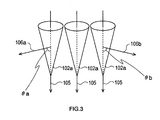
- FIG. 3 is a schematic perspective view illustrating the inclination state of the side face of each structural element, having the shape of a protrusion, of the antireflection structure in accordance with Figs. 1 and 2 .
- the angles formed by the normal vectors 106a and 106b of the side face of the cone serving as each structural element 102a with respect to the reference vector 105 in the direction from the reference face 103 to the tip of each structural element 102a are ⁇ a and ⁇ b, respectively
- the antireflection structure 102 comprising the structural elements arranged at a period of 0.15 ⁇ m and having the shape of a cone with a height of 0.15 ⁇ m (corresponding to the period)
- 63.4 degrees ⁇ ⁇ ⁇ 90 degrees is obtained in consideration of the fact that the structural elements
- a method for producing the light-absorbing member 100 For example, a pattern is drawn on a quartz glass substrate or the like by the electronic beam drawing method or the like and subjected to dry etching or other processing, and a high-precision master mold precision-machined so as to have the same shape as that of the antireflection structure 102 is made beforehand. A glass material heated and softened is subjected to pressure molding using this master mold, whereby a mold for molding antireflection structures is formed of glass.
- the substrate 101 made of a black resin material is produced by pressure molding using this mold for molding antireflection structures, the light-absorbing member 100 can be produced at low cost in large quantity.
- the light-absorbing member 100 is made by providing the microscopic antireflection structure 102 formed at a period smaller than the wavelength of the light whose reflection should be reduced on the surface of the substrate 101 as described above, the reflection of light at the interface with air can be prevented and incident light can be absorbed substantially completely by using this light-absorbing member 100.
- the light-absorbing member 100 is advantageous when it is separated from the mold during pressure molding, in particular.
- the respective structural elements of the antireflection structure 102 are arranged so that the straight lines 104 connecting the reference face 103 to the tips of the respective structural elements 102a are nearly parallel to one another, the light-absorbing member 100 can be separated from the mold without damaging the antireflection structure 102 during pressure molding.
- an antireflection structure having cones with a height corresponding to the period or more is formed; however, light-absorbing efficiency can be raised further by forming an antireflection structure having cones with a height corresponding to two or three times the period or more.
- visible light is used as the light whose reflection should be reduced; however, other than visible light, ultraviolet light (the wavelength of ultraviolet spectrum: 70 nm to 400 nm), near-infrared light (the wavelength of near-infrared spectrum: 700 nm to 2 ⁇ m) and far-infrared light (the wavelength of far-infrared spectrum: 2 ⁇ m to 13 ⁇ m) can also be used; even in this case, the antireflection structure is formed at a period smaller than the respective wavelengths. Even in this case, the height of the structural element is desired to be a height corresponding to the period or more, two times the period or more, or three times the period or more.
- the substrate 101 made of a black material is obtained by including a dye, such as a black dye (for example, Plast Black 8950 or 8970 produced by Arimoto Chemical Co., Ltd.) obtained by mixing cyan, magenta, yellow and other coloring matters, in a base material, such as polycarbonate resin or acrylic resin; however, the substrate can also be obtained by including a pigment, such as carbon black.
- a black dye for example, Plast Black 8950 or 8970 produced by Arimoto Chemical Co., Ltd.
- a base material such as polycarbonate resin or acrylic resin
- the substrate can also be obtained by including a pigment, such as carbon black.
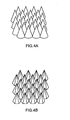
- an antireflection structure comprising structural elements having the shape of a cone (see FIG. 4A ) is taken as an example and described; however, the antireflection structure is not necessary limited to this configuration.
- the structural element may have the shape of a pyramid (see FIG. 4B ), such as a regular hexagonal pyramid or a quadrangular pyramid.
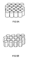
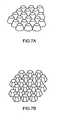
- the shape of the structural element of the antireflection structure is not necessarily limited to a cone or a pyramid, but the shape may be a columnar shape, such as a cylinder (see FIG. 5A ) or a prism (see FIG. 5B ), a bell shape rounded at the tip (see FIGS.
- the structural element is not required to have a strictly geometrical shape, but its shape should only substantially be a cone or pyramid, a column, a bell, or a truncated cone or pyramid.
- the structural elements of the antireflection structure 102 should only be arranged at least at a period smaller than the wavelength of the light whose reflection should be reduced.
- the antireflection structure 102 a structure comprising structural elements formed of protrusions having the shape of a cone is shown; however, the structure is not limited to this.
- an antireflection structure wherein recesses having the shape of a cone are formed in an array form in a flat face may also be formed.
- FIG. 8 is a schematic cross-sectional view showing a comparative light-absorbing member , being cut off by a plane perpendicular to the longitudinal direction thereof.
- the light-absorbing member 110 comprises a substrate 111 and an antireflection structure 112. Since the light-absorbing member 110 in accordance with the comparative example is identical to the light-absorbing member 100 in accordance with the first comparative example described above with respect to schematic configuration, the differences therebetween will be described mainly.
- a recess having the shape of a cone of 0.15 ⁇ m in depth is used as a structural element, and these cones are disposed on the surface of the substrate 111 in an array form at a period of 0.15 ⁇ m.
- the period between the cones herein corresponds to a period smaller than the wavelength of the visible spectrum (400 nm to 700 nm).
- the depth of these cones corresponds to the period or more. Since the antireflection structure 112 of the light-absorbing member 110 has the above-mentioned configuration, even if light having a wavelength of the visible spectrum or longer enters, the light is not reflected but can be absorbed by the substrate 111 substantially completely.
- each of the structural elements 112a has a shape being recessed from a reference face 113 corresponding to the macroscopic curve of the substrate.
- the structural elements 112a are arranged so that the straight lines connecting the reference face 113 to the tips of the respective structural elements 112a are nearly parallel to one another.
- the straight line corresponds to the straight line connecting the center of the bottom face of the cone of each structural element 112a to the vertex of the cone and is the center axis of the cone.
- each structural element 112a of the antireflection structure 112 in accordance with this comparative example has a shape such that when the structural element is viewed from the direction of the straight line serving as a specific reference direction common to all the structural elements, the whole area of its side face can be seen.
- ultraviolet light the wavelength of ultraviolet spectrum: 70 nm to 400 nm
- near-infrared light the wavelength of near-infrared spectrum: 700 nm to 2 ⁇ m
- far-infrared light the wavelength of far-infrared spectrum: 2 ⁇ m to 13 ⁇ m
- the antireflection structure is formed at a period smaller than the respective wavelengths.
- the depth of the structural element is desired to be a depth corresponding to the period or more, two times the period or more, or three times the period or more.
- the structural element is not limited to have the shape of a cone, but the shape may be a pyramid, a cylinder, a prism, a bell, a truncated cone, a truncated pyramid or the like. Still further, the structural element is not required to have a strictly geometrical shape, but its shape should only substantiallybe the shape of a cone or pyramid, a column, a bell, or a truncated cone or pyramid, as in the above-mentioned case.
- FIG. 9 is a schematic cross-sectional view showing a lens barrel in accordance with an embodiment of the present invention, being cut off by a plane perpendicular to the optical axis thereof
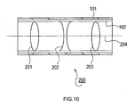
- FIG. 10 is a schematic cross-sectional view showing the lens barrel (with lenses mounted), being cut off by a plane including the optical axis thereof.
- the lens barrel 200 in accordance with this embodiment has a structure wherein the light-absorbing members 100 (seeFIG. 1), four in number and described above, are prepared and integrated into the shape of a cylinder.
- the lens barrel 200 in accordance with this embodiment coaxially holds a lens element 201, a lens element 202 and a lens element 203 along the optical axis 204. Since the antireflection structure 102 is formed on the internal circumference face of the lens barrel 200, unnecessary light, such as stray light generated by a luminous flux entering the lens element 201 held inside the lens barrel 200 and having an angle not smaller than the coverage view angle and by reflection on the surfaces of the respective lens elements, is absorbed efficiently by the substrate via the antireflection structure 102. As a result, the unnecessary light can be prevented from entering again the optical path, whereby the generation of ghost and flare is suppressed in the optical system comprising the respective lens elements. In particular, when the optical system is an image-taking optical system of a digital camera or an imaging optical system, such as the projection optical system of a projection image display apparatus, an optical image being excellent in contrast can be formed.
- unnecessary light may occasionally have a constant regularity in a lens barrel or the like.
- unnecessary light may occasionally have a constant regularity in a lens barrel or the like.
- stray light abundantly enters the internal face of the lens barrel 200 in the normal direction
- a slight difference occurs in the effect of reducing reflection between the effect at a position near the central area wherein the antireflection structure 102 is formed and the effect at a position near the periphery thereof (near the boundary with another adjacent light-absorbing member) owing to the difference in the incident angle of the unnecessary light entering the light-absorbing member.
- the height or depth of each of the structural elements of the antireflection structure 102 is varied so that the height or depth of each of the structural elements increases gradually in the area from the position near the central area wherein the antireflection structure 102 is formed to the position near the periphery thereof (near the boundary with another adjacent light-absorbing member).
- the lens barrel 200 having the side face shape of a cylinder is taken as an example and described; however, the side face shape of the lens barrel 200 is not limited to a cylinder, but it may be a truncated cone, for example.
- the lens barrel 200 formed of a single cylinder is taken as an example and described; however, the lens barrel is applicable to a collapsible lens barrel comprising a plurality of cylindrical members combined so as to be slidable.
- a structure wherein a plurality of the light-absorbing members 100 described above are prepared and integrated into the shape of a cylinder is taken as an example and described; however, the structure is not limited to this.
- an antireflection structure may be formed on a flexible sheet member, and the sheet member may be bonded to the internal circumference face of the main body of the lens barrel.
- the sheet member can be made of a black material.
- the sheet member made of a black material can be obtained by including a dye, such as a black dye (for example, Plast Black 8950 or 8970 produced by Arimoto Chemical Co., Ltd.) obtained by mixing cyan, magenta, yellow and other coloring matters, into a base material, such as polycarbonate resin or acrylic resin. Moreover, the sheet member can also be obtained by including a pigment, such as carbon black. Still further, instead of the entire internal circumference face of the lens barrel, at least part thereof may be formed of the light-absorbing member 100 or the light-absorbing member 110 described above. Still further, in this embodiment, the internal face of the lens barrel 200 is divided into four areas in the longitudinal direction thereof; however, the number of the divisions is a given number, and the internal face should only be divided into at least three areas.
- a black dye for example, Plast Black 8950 or 8970 produced by Arimoto Chemical Co., Ltd.
- FIG. 11 is a schematic cross-sectional view showing a lens barrel forming mold , being cut off by a plane perpendicular to the longitudinal direction thereof.
- the lens barrel forming mold shown in FIG. 11A is a first mold 301 to be set first on the substrate of the lens barrel
- the lens barrel forming mold shown in FIG. 11B is a second mold 302 to be set on the substrate of the lens barrel after the first mold 301 is set.
- FIG. 12 is a schematic cross-sectional view showing the state at the time when the lens barrel forming mold is set on the substrate of the lens barrel, being cut off by a plane perpendicular to the optical axis thereof.
- each of the first and second molds 301 and 302 is configured so as to form part of the side face of a cylinder, and two of each are prepared.
- the first and second molds 301 and 302 are obtained by dividing a single cylinder into four pieces in the longitudinal direction thereof.
- both sides of the first and second molds 301 and 302 are processed into shapes such that they do not interfere with each other when the first and second molds 301 and 302 are set on the substrate 101 of the lens barrel 200 in the above-mentioned sequence (see FIG. 12 ).
- an antireflection structure having a pattern inverted from that of the antireflection structure 102 on the internal face of the lens barrel 200 that is, an antireflection structure 303 comprising structural elements formed of recesses having the shape of a cone and arranged at a period smaller than the wavelength of the light whose reflection should be reduced is formed.
- the center axes of the recesses, each serving as a structural element, are parallel to one another.
- the antireflection structures 303 of the first and second molds 301 and 302 serving as the lens barrel forming mold are desired to be formed using X-rays.
- the amount of the sag of the external surface of each of the molds 301 and 302 becomes 4.39 mm.
- the maximum inclination angle of the internal face of the cone serving as each of the structural elements of the antireflection structure 303 is 45 degrees, it is difficult to form the antireflection structure 303 on the external surface of each of the molds 301 and 302 using the two-beam interference exposure method.
- the antireflection structure 303 can be formed by using the X-ray exposure method. More specifically, the surface of a substrate formed of a high molecular compound having a property of being photosensitive to X-rays, such as poly(methyl methacrylate) (PMMA), is exposed with X-rays having an energy of 1 kJ/cm 3 to 20 kJ/cm 3 , and the surface is nickel-plated, and then the substrate is removed, whereby a metal portion having the antireflection structure 303 is obtained; hence, the lens barrel forming mold (the first and second molds 301 and 302) should be produced by using this.
- PMMA poly(methyl methacrylate)
- the antireflection structure 303 is formed by using X-rays is described above; however, it is also possible to form the antireflection structure 303 by using ultraviolet light or light having a wavelength smaller than that of ultraviolet light.
- formylated novolac resin should be used as a high molecular compound having a property of being photosensitive to ultraviolet light or light having a wavelength smaller than that of ultraviolet light.
- two first molds 301 are set on the internal surface of the substrate 101.
- two second molds 302 are set on the internal surface of the substrate 101, each disposed between the two first molds 301, and the patterns of the antireflection structure 303 formed on the external surfaces of the first and second molds 301 and 302 are transferred to the internal surface of the substrate 101 (see FIG. 12 ).
- the whole is cooled, and the first and second molds 301 and 302 are separated.
- the lens barrel 200 having the microscopic antireflection structure 303 formed on the internal surface of the substrate 101 at a period smaller than the wavelength of incident light is obtained.
- the center axes of the cones, each serving as the structural element are parallel to one another; hence, by separating the second mold 302 and the first mold 301 in this sequence in the direction of each center axis, the lens barrel 200 can be formed without damaging the respective antireflection structures 102.
- the number of the divisions of the lens barrel forming mold is four; however, the number of the divisions can be made appropriate if it is three or more.
- the lens barrel forming mold having the antireflection structure 303 formed on the external surface thereof is taken as an example and described; however, when a lens barrel having an antireflection structure on the external surface thereof is formed, a lens barrel forming mold having an antireflection structure formed on the internal surface thereof is used.
- the antireflection structure of the lens barrel forming mold is not limited to the structure described, but any structures can be used if these antireflection structures are configured so that they can be separated from the mold in one direction without being damaged.
- first and second molds 301 and 302, each configured to form part of the side face of a cylinder are taken as examples ; however, when a lens barrel having the shape of a truncated cone is formed, molds, each configured to form part of the side face of a truncated cone, are used.
- the light-absorbing member in accordance with the present invention is applicable to all the optical apparatuses requiring elimination of unnecessary light, for example, projection display devices, such as front projectors and rear projectors; multivision systems provided with a plurality of such projection display devices; image-taking devices, such as digital still cameras and camcorders; optical pickup devices; optical fiber communication systems; etc.
- projection display devices such as front projectors and rear projectors
- multivision systems provided with a plurality of such projection display devices
- image-taking devices such as digital still cameras and camcorders
- optical pickup devices optical fiber communication systems
Landscapes
- Physics & Mathematics (AREA)
- General Physics & Mathematics (AREA)
- Optics & Photonics (AREA)
- Lens Barrels (AREA)
- Surface Treatment Of Optical Elements (AREA)
- Optical Elements Other Than Lenses (AREA)
- Laminated Bodies (AREA)
Claims (11)
- Lichtabsorbierendes Element (100), umfassend:ein Substrat (101), welches aus einem schwarzen Material hergestellt ist, welches sichtbares Licht absorbieren kann, dessen Reflexion verhindert werden soll, wobei das Substrat (101) von einem makroskopischen Blickpunkt aus betrachtet die Form eines Bogens aufweist; undeine Antireflexionsstruktur (102), welche Strukturelemente (102a) umfasst, welche auf der Oberfläche des Bogens in einer Matrixform mit einer Periode angeordnet sind, welche kleiner als die Wellenlänge des sichtbaren Lichts ist, wobeidie Strukturelemente (102a) eine konische Form aufweisen, welche von einer dem Bogen des Substrats (101) entsprechenden Referenzfläche (103, 113) vorspringt oder ausgenommen ist, und derart angeordnet sind, dass die geraden Linien (104), welche die Referenzfläche (103, 113) mit den Eckpunkten der entsprechenden Strukturelemente (102a) verbinden, zueinander nahezu parallel sind, undeine Höhe oder Tiefe eines jeden der Strukturelemente (102a) der Antireflexionsstruktur (102) derart variiert, dass die Höhe oder Tiefe graduell von einer Position nahe einem Mittelbereich in einem Bereich, in welchem die Antireflexionsstruktur (102) gebildet ist, zu einer Position nahe einem Rand in dem Bereich zunimmt.
- Lichtabsorbierendes Element (100) gemäß Anspruch 1, wobei jedes der Strukturelemente (102a) eine Beziehung von e < 90 Grad erfüllt,
wobei θ einen Winkel darstellt, welcher durch den Normalenvektor der Seitenfläche der vorspringenden konischen Form oder der Innenfläche der ausgenommenen konischen Form mit Bezug auf den Referenzvektor in die Richtung von der Referenzfläche (113) zum Eckpunkt jedes Strukturelements (102a) gebildet wird. - Lichtabsorbierendes Element (100) gemäß Anspruch 1, wobei die Antireflexionsstruktur (102) einstückig als Teil des Substrats (101) gebildet ist.
- Lichtabsorbierendes Element (100) gemäß Anspruch 1, wobei die Antireflexionsstruktur (102) auf einem mit dem Substrat (101) verbundenen Plattenelement gebildet ist.
- Lichtabsorbierendes Element (100) gemäß Anspruch 1, wobei die Länge zwischen der Referenzfläche (103, 113) und dem Eckpunkt von jedem der entsprechenden Strukturelemente (102a) in die Richtung entlang der geraden Linie (104) der Periode oder mehr entspricht.
- Lichtabsorbierendes Element (100) gemäß Anspruch 1, wobei die Form des Bogens eine Absenkung ist.
- Lichtabsorbierendes Element (100) gemäß Anspruch 1, wobei die Höhe einer Senkung der Oberfläche des Bogens 20 µm oder mehr ist.
- Lichtabsorbierendes Element (100) gemäß Anspruch 1, wobei in jedem der Strukturelemente (102a) die untere Fläche des konischen Vorsprungs an der Referenzfläche (103) oder die obere Fläche der konischen Ausnehmung in der Referenzfläche (113) eine Form aufweist, welche aus der Gruppe ausgewählt ist, welche aus einer kreisförmigen Form, einer elliptischen Form, einer rechteckigen Form und einer polygonalen Form besteht.
- Lichtabsorbierendes Element (100) gemäß Anspruch 1, wobei das Substrat (101) einen Farbstoff enthält.
- Lichtabsorbierendes Element (100) gemäß Anspruch 1, wobei das Substrat (101) ein Pigment enthält.
- Objektivtubus (200), wobei vier lichtabsorbierende Elemente (100) gemäß Anspruch 1 in die Form eines Zylinders integriert sind.
Applications Claiming Priority (2)
| Application Number | Priority Date | Filing Date | Title |
|---|---|---|---|
| JP2004158221 | 2004-05-27 | ||
| PCT/JP2005/009293 WO2005116695A1 (en) | 2004-05-27 | 2005-05-16 | Light-absorbing member |
Publications (2)
| Publication Number | Publication Date |
|---|---|
| EP1749221A1 EP1749221A1 (de) | 2007-02-07 |
| EP1749221B1 true EP1749221B1 (de) | 2013-02-20 |
Family
ID=34970814
Family Applications (1)
| Application Number | Title | Priority Date | Filing Date |
|---|---|---|---|
| EP05741139A Ceased EP1749221B1 (de) | 2004-05-27 | 2005-05-16 | Lichtabsorptionsglied |
Country Status (5)
| Country | Link |
|---|---|
| US (1) | US7850319B2 (de) |
| EP (1) | EP1749221B1 (de) |
| JP (1) | JP4608501B2 (de) |
| CN (1) | CN100427971C (de) |
| WO (1) | WO2005116695A1 (de) |
Families Citing this family (47)
| Publication number | Priority date | Publication date | Assignee | Title |
|---|---|---|---|---|
| JP2007264594A (ja) * | 2006-03-01 | 2007-10-11 | Nissan Motor Co Ltd | 反射防止微細構造、反射防止成形体及びその製造方法 |
| DE102006013670A1 (de) * | 2006-03-24 | 2007-09-27 | X-Fab Semiconductor Foundries Ag | Breitbandig entspiegelte optische Bauteile mit gekrümmten Oberflächen |
| JP5105771B2 (ja) * | 2006-05-15 | 2012-12-26 | パナソニック株式会社 | 反射防止構造体及びそれを備えた光学装置 |
| JP4794351B2 (ja) * | 2006-05-15 | 2011-10-19 | パナソニック株式会社 | 反射防止構造体及びそれを備えた光学装置 |
| JP2007304466A (ja) * | 2006-05-15 | 2007-11-22 | Matsushita Electric Ind Co Ltd | 光吸収性反射防止構造体、それを備えた光学ユニット及びレンズ鏡筒ユニット、並びにそれらを備えた光学装置 |
| JP5383188B2 (ja) * | 2006-06-21 | 2014-01-08 | パナソニック株式会社 | レンズ鏡筒 |
| WO2009031299A1 (ja) * | 2007-09-03 | 2009-03-12 | Panasonic Corporation | 反射防止構造体、光学ユニット及び光学装置 |
| CN101452101A (zh) | 2007-12-06 | 2009-06-10 | 鸿富锦精密工业(深圳)有限公司 | 镜头模组及相机模组 |
| JP5211165B2 (ja) * | 2008-07-04 | 2013-06-12 | アルプス電気株式会社 | 反射防止構造を有する光学部品および前記光学部品の製造方法 |
| GB2465607A (en) * | 2008-11-25 | 2010-05-26 | St Microelectronics | CMOS imager structures |
| US9435916B2 (en) | 2008-12-30 | 2016-09-06 | 3M Innovative Properties Company | Antireflective articles and methods of making the same |
| JP5940809B2 (ja) * | 2008-12-30 | 2016-06-29 | スリーエム イノベイティブ プロパティズ カンパニー | ナノ構造化物品及びナノ構造化物品の作製方法 |
| JP5108151B2 (ja) * | 2009-07-28 | 2012-12-26 | シャープ株式会社 | 光学フィルム、その製造方法及びその光学特性を制御する方法 |
| JP5490216B2 (ja) * | 2010-03-02 | 2014-05-14 | パナソニック株式会社 | 光学素子及び光学素子の製造方法 |
| US20120001061A1 (en) * | 2010-07-02 | 2012-01-05 | Hamilton Sundstrand Corporation | Ion implanted beam dump |
| JP2012058584A (ja) * | 2010-09-10 | 2012-03-22 | Tohoku Univ | 反射防止光学構造付き基板および反射防止光学構造付き基板の製造方法 |
| US20120268822A1 (en) * | 2011-04-19 | 2012-10-25 | Bee Khuan Jaslyn Law | Antireflective hierarchical structures |
| TWI453927B (zh) * | 2011-06-29 | 2014-09-21 | Ind Tech Res Inst | 多重反射結構以及光電元件 |
| JP2015018005A (ja) * | 2011-11-11 | 2015-01-29 | パナソニック株式会社 | レンズ鏡筒 |
| JP2013254130A (ja) * | 2012-06-08 | 2013-12-19 | Dexerials Corp | 光学素子およびその製造方法、表示素子、ならびに投射型画像表示装置 |
| JP6281234B2 (ja) * | 2012-12-26 | 2018-02-21 | 凸版印刷株式会社 | 電子ビーム描画装置 |
| KR101306895B1 (ko) * | 2013-02-21 | 2013-09-10 | 송연희 | 패턴을 갖는 렌즈의 제조방법 |
| JP6568424B2 (ja) * | 2014-08-27 | 2019-08-28 | 積水化学工業株式会社 | 赤外線カットフィルタ及び赤外線カットフィルタの製造方法 |
| KR101740775B1 (ko) * | 2014-12-23 | 2017-05-26 | 삼성전기주식회사 | 렌즈 조립체 및 이를 구비하는 카메라 모듈 |
| JP6689576B2 (ja) * | 2015-03-31 | 2020-04-28 | デクセリアルズ株式会社 | 原盤の製造方法、原盤、及び光学体 |
| JP6032446B1 (ja) * | 2015-05-22 | 2016-11-30 | 尾池工業株式会社 | 低反射グラフェン、光学部材用低反射グラフェン |
| US10197800B2 (en) * | 2015-09-25 | 2019-02-05 | Everready Precision Ind. Corp. | Optical lens |
| KR101863528B1 (ko) * | 2016-11-21 | 2018-05-31 | 오오쯔까 테크노 코포레이션 | 반사 방지 구조체, 카메라 유닛, 휴대 기기 및 반사 방지 구조체의 제조방법 |
| EP3647046A4 (de) * | 2017-06-27 | 2021-03-17 | LG Chem, Ltd. | Dekoratives element und verfahren zur herstellung davon |
| KR102201549B1 (ko) * | 2017-06-27 | 2021-01-12 | 주식회사 엘지화학 | 장식 부재 및 이의 제조방법 |
| US11380438B2 (en) | 2017-09-27 | 2022-07-05 | Honeywell International Inc. | Respiration-vocalization data collection system for air quality determination |
| US11209577B2 (en) * | 2018-05-30 | 2021-12-28 | Ocean Optics, Inc. | Macro-scale features for optically black surfaces and straylight suppression |
| CN208636512U (zh) * | 2018-08-08 | 2019-03-22 | 瑞声科技(新加坡)有限公司 | 一种镜头模组 |
| US10876949B2 (en) | 2019-04-26 | 2020-12-29 | Honeywell International Inc. | Flow device and associated method and system |
| CN111948775B (zh) * | 2019-05-15 | 2023-04-14 | 大立光电股份有限公司 | 塑胶镜筒、相机模块及电子装置 |
| US10794810B1 (en) | 2019-08-02 | 2020-10-06 | Honeywell International Inc. | Fluid composition sensor device and method of using the same |
| KR20210053603A (ko) * | 2019-11-04 | 2021-05-12 | 삼성전기주식회사 | 카메라 모듈 및 휴대 단말기 |
| US11333593B2 (en) | 2020-02-14 | 2022-05-17 | Honeywell International Inc. | Fluid composition sensor device and method of using the same |
| US11391613B2 (en) | 2020-02-14 | 2022-07-19 | Honeywell International Inc. | Fluid composition sensor device and method of using the same |
| US12164170B2 (en) * | 2020-03-25 | 2024-12-10 | Samsung Electro-Mechanics Co., Ltd. | Spacer and lens assembly including spacer |
| CN113805299B (zh) * | 2020-06-11 | 2024-11-22 | 玉晶光电(厦门)有限公司 | 垫圈 |
| US12111257B2 (en) * | 2020-08-26 | 2024-10-08 | Honeywell International Inc. | Fluid composition sensor device and method of using the same |
| US11835432B2 (en) | 2020-10-26 | 2023-12-05 | Honeywell International Inc. | Fluid composition sensor device and method of using the same |
| US12281976B2 (en) | 2021-05-13 | 2025-04-22 | Honeywell International Inc. | In situ fluid sampling device and method of using the same |
| CN114415456B (zh) * | 2021-12-22 | 2024-05-14 | 歌尔光学科技有限公司 | 一种投影光机以及设计方法 |
| KR20230173878A (ko) * | 2022-06-20 | 2023-12-27 | 삼성전기주식회사 | 렌즈 조립체 |
| WO2025080517A1 (en) * | 2023-10-11 | 2025-04-17 | Apple Inc. | Camera modules with micro-scale optically absorptive gratings |
Family Cites Families (29)
| Publication number | Priority date | Publication date | Assignee | Title |
|---|---|---|---|---|
| GB1462618A (en) * | 1973-05-10 | 1977-01-26 | Secretary Industry Brit | Reducing the reflectance of surfaces to radiation |
| US4111762A (en) * | 1975-01-31 | 1978-09-05 | Martin Marietta Corporation | Optically black coating and process for forming it |
| GB1588370A (en) * | 1978-05-11 | 1981-04-23 | Standard Telephones Cables Ltd | Infra-red transmitting elements |
| US4396643A (en) * | 1981-06-29 | 1983-08-02 | Minnesota Mining And Manufacturing Company | Radiation absorbing surfaces |
| US4589972A (en) * | 1984-07-30 | 1986-05-20 | Martin Marietta Corporation | Optically black coating with improved infrared absorption and process of formation |
| JPS6296902A (ja) * | 1985-10-24 | 1987-05-06 | Seiko Epson Corp | 反射防止プラスチツク |
| US4812352A (en) * | 1986-08-25 | 1989-03-14 | Minnesota Mining And Manufacturing Company | Article having surface layer of uniformly oriented, crystalline, organic microstructures |
| US5039561A (en) * | 1986-08-25 | 1991-08-13 | Minnesota Mining And Manufacturing Company | Method for preparing an article having surface layer of uniformly oriented, crystalline, organic microstructures |
| US5212596A (en) * | 1992-05-18 | 1993-05-18 | Battelle Memorial Institute | Nonreflective articles |
| US5225933A (en) * | 1992-05-18 | 1993-07-06 | Battelle Memorial Institute | Ultrablack surfaces |
| JPH05341167A (ja) * | 1992-06-08 | 1993-12-24 | Matsushita Electric Ind Co Ltd | レンズ保持部材と薄膜形成方法 |
| WO1995023710A1 (en) | 1994-03-02 | 1995-09-08 | Applied Physics Research, L.P. | Light control material and method for making same |
| IT1281359B1 (it) | 1995-09-26 | 1998-02-18 | Fiat Ricerche | Superficie anti-riflettente a rugosita' predeterminata, particolarmente per plance di autoveicoli |
| JPH11242150A (ja) * | 1998-02-26 | 1999-09-07 | Mitsubishi Electric Corp | 投写型表示装置 |
| JP3368225B2 (ja) * | 1999-03-11 | 2003-01-20 | キヤノン株式会社 | 回折光学素子の製造方法 |
| US6326723B1 (en) | 1999-05-25 | 2001-12-04 | Intel Corporation | Display screen |
| US6175442B1 (en) * | 1999-05-25 | 2001-01-16 | Intel Corporation | Anti-reflection layer in spatial light modulators |
| JP3328238B2 (ja) | 1999-08-27 | 2002-09-24 | エヌイーシービューテクノロジー株式会社 | 単板反射型素子を用いた高輝度プロジェクタ |
| US6603262B2 (en) * | 1999-12-09 | 2003-08-05 | Matsushita Electric Industrial Co., Ltd. | Electrode plate and manufacturing method for the same, and gas discharge panel having electrode plate and manufacturing method for the same |
| GB2360971A (en) * | 2000-04-03 | 2001-10-10 | Suisse Electronique Microtech | Technique for microstructuring replication moulds |
| JP4197100B2 (ja) * | 2002-02-20 | 2008-12-17 | 大日本印刷株式会社 | 反射防止物品 |
| JP4002453B2 (ja) | 2002-03-12 | 2007-10-31 | 株式会社きもと | 光吸収性部材 |
| JP2003279705A (ja) * | 2002-03-25 | 2003-10-02 | Sanyo Electric Co Ltd | 反射防止部材 |
| JP4018440B2 (ja) | 2002-05-07 | 2007-12-05 | キヤノン株式会社 | 観察光学系および光学機器 |
| JP2004012856A (ja) * | 2002-06-07 | 2004-01-15 | Nippon Sheet Glass Co Ltd | 光学素子、光学素子の成形型および光学素子の製造方法 |
| EP1679532A1 (de) * | 2003-10-29 | 2006-07-12 | Matsushita Electric Industrial Co., Ltd. | Optisches element mit antireflexstruktur und verfahren zur herstellung eines optischen elements mit antireflexstruktur |
| US7252869B2 (en) * | 2003-10-30 | 2007-08-07 | Niyaz Khusnatdinov | Microtextured antireflective surfaces with reduced diffraction intensity |
| CN1930497A (zh) * | 2004-03-12 | 2007-03-14 | 松下电器产业株式会社 | 光吸收构件 |
| WO2006059686A1 (ja) * | 2004-12-03 | 2006-06-08 | Sharp Kabushiki Kaisha | 反射防止材、光学素子、および表示装置ならびにスタンパの製造方法およびスタンパを用いた反射防止材の製造方法 |
-
2005
- 2005-05-16 EP EP05741139A patent/EP1749221B1/de not_active Ceased
- 2005-05-16 JP JP2006544760A patent/JP4608501B2/ja not_active Expired - Fee Related
- 2005-05-16 WO PCT/JP2005/009293 patent/WO2005116695A1/en not_active Ceased
- 2005-05-16 US US11/597,651 patent/US7850319B2/en not_active Expired - Lifetime
- 2005-05-16 CN CNB2005800169343A patent/CN100427971C/zh not_active Expired - Fee Related
Also Published As
| Publication number | Publication date |
|---|---|
| US20070247718A1 (en) | 2007-10-25 |
| JP2008500560A (ja) | 2008-01-10 |
| JP4608501B2 (ja) | 2011-01-12 |
| EP1749221A1 (de) | 2007-02-07 |
| CN100427971C (zh) | 2008-10-22 |
| CN1961224A (zh) | 2007-05-09 |
| WO2005116695A1 (en) | 2005-12-08 |
| US7850319B2 (en) | 2010-12-14 |
Similar Documents
| Publication | Publication Date | Title |
|---|---|---|
| US7850319B2 (en) | Light-absorbing member | |
| US20070195417A1 (en) | Light-absorbing member | |
| US8102609B2 (en) | Lens barrel and image pickup unit | |
| US7262912B2 (en) | Front-projection screens including reflecting layers and optically absorbing layers having apertures therein, and methods of fabricating the same | |
| JP6317954B2 (ja) | レンズユニット、撮像モジュール、及び電子機器 | |
| US7110643B2 (en) | Micro lens array and a method of manufacturing a replication mold for the same | |
| US7031064B2 (en) | Method of microlens array and projection type of liquid crystal display apparatus | |
| CN101082680B (zh) | 光吸收防反射构造体,光学单元,透镜镜筒单元和光学装置 | |
| JP2015068853A (ja) | 積層体、撮像素子パッケージ、撮像装置および電子機器 | |
| EP1766465A1 (de) | Optische einrichtung für ein display mit verjüngtem wellenleiter und herstellungsprozess dafür | |
| US6480345B2 (en) | Image magnifying/reducing optical device and manufacturing method thereof | |
| CN104422972B (zh) | 光学元件、摄像装置、光学设备、原盘及制造方法 | |
| US7787184B2 (en) | Member having antireflection structure | |
| EP4198377A1 (de) | Optisches system, anzeigevorrichtung, projektionsvorrichtung und beleuchtungsvorrichtung | |
| US20150276990A1 (en) | Optical device, original plate, method of manufacturing original plate, and imaging apparatus | |
| TWI820748B (zh) | 成像透鏡組、相機模組與電子裝置 | |
| CN217181265U (zh) | 匀光片和光学装置 | |
| CN114706184A (zh) | 一种光学成像镜头 | |
| CN115914804B (zh) | 成像组件及其制造方法和摄像模组、电子设备 | |
| US20240288613A1 (en) | Optical element, optical apparatus, and method for manufacturing optical element | |
| CN117201919A (zh) | 一种摄像头模组及电子设备 | |
| CN119596630A (zh) | 一种投影屏幕、投影设备、微结构透镜模具及其制作方法 | |
| KR20050003980A (ko) | 투사광학계, 프로젝션 텔레비전 및 투사광학계의 렌즈제조 방법 | |
| TW200928482A (en) | Lens module |
Legal Events
| Date | Code | Title | Description |
|---|---|---|---|
| PUAI | Public reference made under article 153(3) epc to a published international application that has entered the european phase |
Free format text: ORIGINAL CODE: 0009012 |
|
| 17P | Request for examination filed |
Effective date: 20061123 |
|
| AK | Designated contracting states |
Kind code of ref document: A1 Designated state(s): DE FR GB |
|
| DAX | Request for extension of the european patent (deleted) | ||
| RBV | Designated contracting states (corrected) |
Designated state(s): DE FR GB |
|
| RAP1 | Party data changed (applicant data changed or rights of an application transferred) |
Owner name: PANASONIC CORPORATION |
|
| 17Q | First examination report despatched |
Effective date: 20110707 |
|
| GRAP | Despatch of communication of intention to grant a patent |
Free format text: ORIGINAL CODE: EPIDOSNIGR1 |
|
| GRAS | Grant fee paid |
Free format text: ORIGINAL CODE: EPIDOSNIGR3 |
|
| GRAA | (expected) grant |
Free format text: ORIGINAL CODE: 0009210 |
|
| AK | Designated contracting states |
Kind code of ref document: B1 Designated state(s): DE FR GB |
|
| REG | Reference to a national code |
Ref country code: GB Ref legal event code: FG4D |
|
| REG | Reference to a national code |
Ref country code: DE Ref legal event code: R096 Ref document number: 602005038208 Country of ref document: DE Effective date: 20130418 |
|
| PLBE | No opposition filed within time limit |
Free format text: ORIGINAL CODE: 0009261 |
|
| STAA | Information on the status of an ep patent application or granted ep patent |
Free format text: STATUS: NO OPPOSITION FILED WITHIN TIME LIMIT |
|
| 26N | No opposition filed |
Effective date: 20131121 |
|
| REG | Reference to a national code |
Ref country code: DE Ref legal event code: R097 Ref document number: 602005038208 Country of ref document: DE Effective date: 20131121 |
|
| REG | Reference to a national code |
Ref country code: FR Ref legal event code: PLFP Year of fee payment: 12 |
|
| REG | Reference to a national code |
Ref country code: FR Ref legal event code: PLFP Year of fee payment: 13 |
|
| REG | Reference to a national code |
Ref country code: FR Ref legal event code: PLFP Year of fee payment: 14 |
|
| PGFP | Annual fee paid to national office [announced via postgrant information from national office to epo] |
Ref country code: GB Payment date: 20220519 Year of fee payment: 18 Ref country code: FR Payment date: 20220523 Year of fee payment: 18 Ref country code: DE Payment date: 20220519 Year of fee payment: 18 |
|
| REG | Reference to a national code |
Ref country code: DE Ref legal event code: R119 Ref document number: 602005038208 Country of ref document: DE |
|
| GBPC | Gb: european patent ceased through non-payment of renewal fee |
Effective date: 20230516 |
|
| PG25 | Lapsed in a contracting state [announced via postgrant information from national office to epo] |
Ref country code: DE Free format text: LAPSE BECAUSE OF NON-PAYMENT OF DUE FEES Effective date: 20231201 Ref country code: GB Free format text: LAPSE BECAUSE OF NON-PAYMENT OF DUE FEES Effective date: 20230516 |
|
| PG25 | Lapsed in a contracting state [announced via postgrant information from national office to epo] |
Ref country code: FR Free format text: LAPSE BECAUSE OF NON-PAYMENT OF DUE FEES Effective date: 20230531 |