EP1751820B1 - Planare antenne mit leitfähigen zapfen über einer grundplatte und/oder mit mindestens einem strahlerelement und entsprechendes herstellungsverfahren - Google Patents
Planare antenne mit leitfähigen zapfen über einer grundplatte und/oder mit mindestens einem strahlerelement und entsprechendes herstellungsverfahren Download PDFInfo
- Publication number
- EP1751820B1 EP1751820B1 EP05759955A EP05759955A EP1751820B1 EP 1751820 B1 EP1751820 B1 EP 1751820B1 EP 05759955 A EP05759955 A EP 05759955A EP 05759955 A EP05759955 A EP 05759955A EP 1751820 B1 EP1751820 B1 EP 1751820B1
- Authority
- EP
- European Patent Office
- Prior art keywords
- radiating element
- radiating
- conductive
- antenna
- flat base
- Prior art date
- Legal status (The legal status is an assumption and is not a legal conclusion. Google has not performed a legal analysis and makes no representation as to the accuracy of the status listed.)
- Expired - Lifetime
Links
Images




Classifications
-
- H—ELECTRICITY
- H01—ELECTRIC ELEMENTS
- H01Q—ANTENNAS, i.e. RADIO AERIALS
- H01Q9/00—Electrically-short antennas having dimensions not more than twice the operating wavelength and consisting of conductive active radiating elements
- H01Q9/04—Resonant antennas
-
- H—ELECTRICITY
- H01—ELECTRIC ELEMENTS
- H01Q—ANTENNAS, i.e. RADIO AERIALS
- H01Q1/00—Details of, or arrangements associated with, antennas
- H01Q1/36—Structural form of radiating elements, e.g. cone, spiral, umbrella; Particular materials used therewith
- H01Q1/38—Structural form of radiating elements, e.g. cone, spiral, umbrella; Particular materials used therewith formed by a conductive layer on an insulating support
-
- H—ELECTRICITY
- H01—ELECTRIC ELEMENTS
- H01Q—ANTENNAS, i.e. RADIO AERIALS
- H01Q1/00—Details of, or arrangements associated with, antennas
- H01Q1/12—Supports; Mounting means
- H01Q1/22—Supports; Mounting means by structural association with other equipment or articles
- H01Q1/24—Supports; Mounting means by structural association with other equipment or articles with receiving set
-
- H—ELECTRICITY
- H01—ELECTRIC ELEMENTS
- H01Q—ANTENNAS, i.e. RADIO AERIALS
- H01Q21/00—Antenna arrays or systems
Definitions
- planar antennas of the type comprising at least one radiating element (also called "patch", planar pattern, radiating pattern or printed pattern) separated from a ground plane by a dielectric.
- radiating elements are among the key components, for which the specifications requested are increasingly binding. It must of course constantly optimize all the electrical performance of these antennas, but also satisfy criteria increasingly critical, such as the size, weight or cost of these components.
- planar solutions appear today as particularly appropriate to meet all the specifications requested. This planar approach offers developers enough flexibility to develop efficient solutions with particularly small dimensions.
- planar antennas of the aforementioned second category are generally, but not necessarily, produced using a printed technology.
- This explains why, historically, the adjective "planar” has been chosen in the expression “planar antenna”, to show an opposition with the traditional antenna structure based on three-dimensional waveguide (3D). is in this context and relates more specifically to an original planar antenna solution in the above sense, as well as a corresponding manufacturing process, to greatly reduce the physical dimension of the basic printed pattern (ie say the radiating element or elements, also called patches).
- the basic principle of most of the solutions implemented to date is to increase the equivalent electrical length of the printed pattern, so that it can radiate at the desired frequency, while reducing its physical dimensions (ie its surface or its volume ).
- the invention particularly aims to provide a technique other than those used until today to increase the equivalent electrical length of the printed pattern (radiating element or patch) of the antenna, so as to obtain a very planar antenna compact.
- a complementary objective of the invention is to provide such a technique which is simple to implement and inexpensive.
- the invention also aims to provide such a technique that can be applied to any type of planar radiating structures, such as the basic antennas "half-wave patches” or “quarter-wave patches”, the antennas “ring patches” , antennas “slotted patches”, antennas PIFA (Planar Inverted-F Antenna) ...
- Another object of the invention is to provide such a technique that can be applied to both a planar antenna with a single radiating element and a planar antenna comprising a superposition of several radiating elements.
- Yet another object of the invention is to provide a planar antenna manufacturing method corresponding, based on very simple integration technologies, which leads to very low cost solutions, quite suitable for development consumer markets.
- the antenna further comprises at least one set of conductive pads connected to and extending from at least one of the elements belonging to the group comprising the ground plane and the said at least one radiating element, in order to reduce at least one physical dimension of said at least one radiating element for a determined resonant frequency.
- the general principle of the invention is therefore simply to have the pads on the ground plane and / or on one or more element (s) radiating (s) (patch (s)) of the planar antenna.
- pad is used in a generic sense, which can be broken down into different variants (and in particular but not exclusively, as detailed in the description below, in the form of a projection, a hole or tongue).
- Dielectric means air or a solid material with characteristics close to those of air, such as for example materials of plastic type, foam, etc.
- these pads locally come to modify the distribution of the electromagnetic field, and make it possible to reduce at least one dimension (the length and / or the width) of the physical element (s) radiating (s) for a fixed resonant frequency.
- the antenna comprises a first set of conductive pads connected to the ground plane and extending towards, without being connected to, said at least one radiating element.
- the antenna is of the type comprising a single radiating element, it advantageously comprises a second set of conductive pads connected to said single radiating element and extending towards, without being connected to, said ground plane.
- the antenna advantageously comprises a third set of conductive pads connected to a first face of said primary radiating element and extending towards, without being connected to, said ground plane.
- the antenna advantageously comprises a fourth set of conductive pads connected to a second face of said primary radiating element and extending towards, without being connected to, another of said radiating elements.
- the antenna advantageously comprises, for at least one of the intermediate radiating elements, a fifth set of conductive pads connected to a first face of said intermediate radiating element and extending towards, without being connected to, another of said radiating elements which follows said intermediate radiating element in a direction of travel of said superposition of the primary radiating element towards the upper radiating element.
- the antenna advantageously comprises, for at least one of the intermediate radiating elements, a sixth set of conductive pads connected to a second face of said intermediate radiating element and extending towards, without being connected to, another one of said radiating elements which precedes said intermediate radiating element in a direction of travel of said superposition of the primary radiating element towards the upper radiating element.
- the antenna advantageously comprises a seventh set of conductive pads connected to a first face said upper radiating element and extending towards, without being connected to, another of said radiating elements which precedes said upper radiating element in a direction of travel of said superposition of the primary radiating element towards the upper radiating element.
- a set of conductive pads extending from the ground plane or respectively one of the radiating elements, intertwine with another set of conductive pads, extending from one of the radiating elements. or respectively another of the radiating elements.
- said radiating element is not connected to any conductive pad in an area where said radiating element is connected with supply means.
- the conductive pads of the same set of conductive pads are distributed in a matrix.
- At least one radiating element to which is connected at least one set of conductive pads is of the type having a symmetry along its two main axes, and in that said conductive pads are distributed in a disposition respecting said symmetry.
- the antenna belongs to the group comprising: planar antennas of the half-wave radiating element type, planar antennas of the quarter-wave radiating element type, planar antennas of the annular radiating element type, planar antennas of the radiating element type with slots written, planar antennas of type radiating element in F-inverted.
- the antenna belongs to the group comprising: planar antennas and non-planar antennas due to non-flatness of the ground plane and / or at least one of the radiating elements.
- At least one of the conductive pads connected to the ground plane or to one of the radiating elements is a conductive projection formed in a first conductive part and extending from a main body. said first conductive part, said main body forming said ground plane or said radiating element.
- At least one of the conductive pads connected to at least one of the radiating elements is a conductive tab, cut in at least an eccentric part of a second conductive part and folded relative to a central part of the second conductive part, said central part forming said radiating element.
- the antenna further comprises at least one support element of said first or second conductive part, made of a dielectric material and for positioning the ground plane with respect to at least one of the radiating elements or for positioning said radiating element with respect to the ground plane or at least one other radiating element.
- At least one of the conductive pads connected to the ground plane or to at least one of the radiating elements is a conductive hole extending from a first face of a layer of dielectric material, said first face carrying said ground plane or said at least one radiating element, said conductive hole extending from said first face and not opening onto a second face of said dielectric material layer, the surface of said hole conductor being covered with a conductive material.
- the invention also relates to a method of manufacturing a planar antenna of the type comprising at least one radiating element separated from a ground plane by a dielectric.
- the method comprises a step of producing at least one set of conductive pads connected to and extending from at least one of the elements belonging to the group comprising the ground plane and said at least one radiating element, so as to reduce at least one physical dimension of said at least one radiating element for a determined resonant frequency.
- the method further comprises a step of positioning said first or second conductive part relative to another element of the antenna, using at least one support element made of a dielectric material.
- a conventional planar antenna comprises at least one radiating element and a ground plane. At least one dielectric separates the radiating element closest to the ground plane and the ground plane itself, as well as the radiating elements between them.
- Dielectric is understood to mean air or a solid material having characteristics close to those of air, such as, for example, materials of plastic type, foam, etc.
- the general principle of the invention is to add to such a conventional planar antenna a plurality of conductive pads connected to and extending from the ground plane and / or one or more radiating elements, so as to reduce minus a physical dimension of the radiating element (s) for a determined resonant frequency.
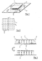
- the figure 1 shows a perspective view of an example of a half-wave patch planar antenna according to the invention, with studs distributed only under the radiating element. These pads 4 are connected to the radiating element 1 and extend towards the ground plane 2 without being connected thereto.
- the antenna is modeled by two radiating slots 5, located at the two ends separated by the half-wave length ( figure 3 ).
- the pads are for example distributed according to a spatial distribution, called matrix, as illustrated in FIG. figure 2 , which is a sectional view of the antenna of the figure 1 along the axis B-B '. This distribution may be uniform or not. In general, any type of arrangement of the pads may be considered, without departing from the scope of the present invention.
- the upper part of the figure 3 is a sectional view of the antenna of the figure 1 along the axis A-A ', making it possible to interpret the effect of the studs positioned under the element beaming.
- the distribution of the electric field between the radiating element 1 and the ground plane 2 is represented by dashed arrows.
- the lower part of the figure 3 is an electrical modeling of the effect of the pads 4 positioned under the radiating element 1.
- the phase velocity of the signal on the radiating pattern 1 decreases, which makes it possible to reduce at least one dimension (the length and / or the physical width of the radiating pattern 1 for a fixed resonant frequency (see hereinafter the reminder of the mathematical reasoning which explains this).
- this decrease in length and / or width depends directly on the number of pads 4 under the radiating pattern 1, as well as their positions and their dimensions (length and diameter).
- the more the number and the length of the studs increase the more the reduction in size becomes important.
- the antenna must be equivalent to a given electrical length ⁇ .
- ⁇ 180 °.
- all conventional excitation means can be envisaged, whether by a simple line section connected on one of the edges of the radiating element and acting as an impedance transformer to correctly adapt the antenna, by a probe connected directly to an equivalent point "50 ⁇ " on the surface of the radiating element or by an excitation solution based on electromagnetic coupling.
- the symmetry along the two main axes (X, Y on the figure 2 ) of the radiating element 1 is respected.
- the studs are distributed according to a provision respecting this symmetry. It is therefore entirely possible to exploit the antenna according to two crossed linear polarizations, or even circular polarization.
- the developed solution, based on pads, is not in itself an obstacle to the use of the antenna for any desired type of polarization.
- planar antennas with studs are given on the Figures 4 and 5 : it is a planar antenna of the quarter-wave patch type, with mass return (referenced 6) located on one of the slices of the support 3 ( figure 4 ), as well as a planar ring-type antenna ( figure 5 ).
- the radiating element (patch) 1 and the pads 4 are produced in a single conductive part 7 (for example a metal part), obtained by machining, stamping or any other method of manufacturing metal parts. dimensional.
- the main body of the conductive part 7 forms the radiating element 1
- the conductive pads 4 are conductive projections formed in the conductive part and which extend from the main body of this part.
- This piece is then transferred to one or more support elements 8, to position it relative to the lower ground plane.
- the dielectric material in which the support element or elements is produced is a plastic material, easily shaped for example by one of the known molding techniques.
- the figure 6 shows an example of an antenna obtained with this first embodiment of the antenna manufacturing method according to the invention, based on the use of a three-dimensional metal part 7 (integrating the radiating element 1 and the pads 4) and The dielectric 3 included in the space between the radiating element 1, on which the conductive pads 4 are connected, and the ground plane 2 is for example air.
- the antenna which may be of foam, plastic material ..., that is to say a layer of dielectric material other than air
- holes vias non-emerging and to cover selectively with a conductive material, the upper face of this substrate (so as to form the radiating element 1), as well as the inside of the holes extending from this upper face (so as to form the conductive pads 4).
- the conductive pads 4 are here made in the form of conductive holes.
- the coating with a conductive material consists of a metallization.
- This metallization can be carried out simply for example by conductive paint deposition or by electrochemical deposition. It is clear, however, that any technique known to those skilled in the art can be used to perform the coating with a conductive material.
- the conductive holes (vias) 4 have an effect similar to that of the conductive pads of the preceding solutions (conductive projections), hence the reduction in the size of the radiating element 1.
- This element (support substrate 3 whose upper face carries the radiating element 1 and has a plurality of metallized holes 4) is then brought into contact, by its lower face, with a ground plane 2 to obtain the final structure of the antenna.
- the support substrate is a plastic material, easily shaped by one of the known molding techniques.
- the figure 7 shows an example of an antenna obtained with this second embodiment of the antenna manufacturing method according to the invention, based on the use of a dielectric substrate 3 whose upper face carries the radiating element 1 and has a plurality of metallized holes forming conductive pads 4.
- the figure 17 shows an example of antenna obtained with this third embodiment of the antenna manufacturing method according to the invention, based on the realization of folded conductive tabs, which form conductive pads 4.
- the positioning of the radiating element relative to the ground plane or vice versa is carried out using one or more supports that may be of the same style as those presented in FIG. figure 6 .
- the support member is other than a dielectric substrate wafer 170 whose height is slightly greater than the height of the tongues to prevent contact between the tongues and the ground plane.
- a first antenna prototype according to the invention of the type, of the antenna presented on the figure 7 , Have been realised.
- This is a half-wave patch solution, printed on a foam material of dimensions 50x50x10mm 3 and reported on a ground plane of 100x100mm 2 .
- the metallization of this upper surface and the interior of the vias is carried out by direct deposition of a conductive silver-based paint (reference: Spraylat 599B3730).
- the figure 8 illustrates experimental results of this first planar antenna prototype according to the invention.
- the antenna has been characterized in adaptation and transmission along the preferred axis of radiation.
- the transmission measurement is based on the implementation of a simple link budget between the developed prototype and a reference antenna (in this case, a printed dipole). It should be noted that, since this link budget is not carried out in an anechoic chamber, the result presented only makes it possible to illustrate the radiation qualitatively.
- the resonant frequency of the antenna according to the invention (with vias non-emerging) is much lower than that of the conventional antenna.
- the levels of adaptation, bandwidth and radiation remain fundamentally correct, as shown by the responses measured on both antennas.
- the technique of the invention (addition of conductive pads 4) thus leads to significant possibilities of miniaturization of the printed pattern (radiating element).
- a second miniature antenna prototype is a quarter-wave patch antenna, with mass return located on one of the slices. of the support.
- This antenna was printed on a substrate of dimensions 25x25x10mm 3 and reported on a ground plane of 100x100mm 2 .
- the mass return is performed by a tab of 5mm width, printed on one of the slices of the foam support substrate and connected at its end to the ground plane.
- the excitation is obtained by coaxial probe connected at a point "50 ⁇ ".
- the figure 10 illustrates experimental results of this second planar antenna prototype according to the invention.
- This second prototype has also been characterized in adaptation and transmission.
- the general principle of the invention (adding pads under the surface of a radiating element in order to reduce at least one dimension (length and / or width) physically for a fixed resonant frequency) can also be used.
- the general principle of the invention (adding pads under the surface of a radiating element in order to reduce at least one dimension (length and / or width) physically for a fixed resonant frequency) can also be used.
- planar antennas with several stacked elements can also be used.
- multi-element antennas are used for example for broadband applications or multifrequency applications.
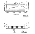
- the figure 12 shows a sectional view of an antenna configuration with two stacked radiating elements, according to the invention.
- This antenna comprises a primary radiating element 1, separated from the ground plane 2 by a first dielectric 3, and an upper radiating element 10, separated from the primary radiating element 1 by a second dielectric 9.
- the primary radiating element is defined as the radiating element closest to the ground plane.
- the upper radiating element is defined as the radiating element furthest from the ground plane.
- the concept of miniaturization according to the invention is applied only to the primary radiating element 1.
- the upper radiating element 10 is not connected to any stud .
- the antenna may comprise any number of superimposed radiating elements and the concept of the invention (addition of conductive pads) may be applied to all the radiating elements of the superposition or to only one or more 'between them.
- the figure 13 is a sectional view of an antenna variant to a radiating element according to the invention.
- the ground plane 132 has conductive pads 135.
- the lower face of the single radiating element 131 also has conductive pads 134.
- These two matrices are located in the area between the upper radiating element and the lower ground plane. To avoid contact between the pads of the two matrices, the first pads are interlaced with the second pads.
- the electrical effect of the pads as described previously is accentuated, which further reduces the physical dimension (length and / or width) of the radiating element for a fixed resonant frequency.
- the concept of the invention can also be applied simultaneously to the two faces of the same radiating element (except for the last of the superposition, that is to say the one farthest from the ground plane).
- the same radiating element may comprise first pads which extend from its lower face and second pads which extend from its upper face.
- the figure 14 is a sectional view of an antenna variant according to the invention, comprising a ground plane 142 and two radiating elements 141, 147.
- the ground plane 142 has conductive pads 144.
- the upper radiating element 147 does not present no plot.
- the primary radiating element 141 has first conductive pads 146 on its lower face and second conductive pads 145 on its upper face.
- the figure 18 is a sectional view of another antenna variant according to the invention, comprising a ground plane 180 and three radiating elements: a primary radiating element 181 (see definition above), an upper radiating element 183 (see definition above) and an intermediate radiating element 182.
- An intermediate radiating element is defined as a radiating element placed between the element radiating primary and the upper radiating element.
- the ground plane 180 and the upper radiating element 183 do not have a stud.
- the primary radiating element 181 has conductive pads 184 on its underside.
- the intermediate radiating element 182 has first conductive pads 185 on its lower face and second conductive pads 186 on its upper face. In general, the fact that the same radiating element has conductive pads on its two faces allows to further miniaturize the antenna. In the same antenna, one can of course have several radiating elements having conductive pads on their two faces.
- planar antenna in the general sense already discussed above, that is to say both planar planar antennas actually flat planar antennas not actually planar (because the ground plane and / or at least one radiating element is not plane but shaped according to a determined three-dimensional shape).
- the figure 15 is a sectional view of another antenna variant according to the invention, comprising a flat ground plane 152 and a radiating element 151 which has conductive pads 154 and is shaped (i.e. three-dimensional non-planar).
- the figure 16 is a sectional view of another antenna variant according to the invention, comprising: a ground plane 162 which has conductive pads 164 and is shaped; and two radiating elements 161, 167, which each have conductive pads 165, 166 and which are shaped.
- the radiating element referenced 161, between the upper radiating element 167 and the ground plane 162, is called primary radiating element.
- the conductive pads are conductive projections ( figure 6 ).
- the conductive pads are conductive holes ( figure 7 ).
- the conductive pads are conductive tabs ( figure 17 ).
- the first and second techniques can be used to make a ground plane with pads.
- the third technique tabs can not be applied to the manufacture of a ground plane comprising conductive pads.
- a same layer of dielectric substrate may carry the ground plane (or a first radiating element) on its lower face and a radiating element (or a second radiating element) on its upper face.
- the pads connected to the ground plane (or to the first radiating element) are made in the form of first conductive holes which extend from the lower face of the substrate layer and do not open on the upper face of the ground layer. substrate.
- the pads connected to the radiating element (or the second radiating element) are made in the form of second conductive holes which extend from the upper face of the substrate layer and do not open on the underside of the layer. of substrate.
- a conductive part which comprises, on the one hand, conductive projections forming first conductive pads and, on the other hand, folded conductive tabs forming second conductive pads.
- the invention is not limited to the embodiments mentioned above. There may be other variants that further minimize the size of the antenna by varying the number, size, shape and layout of the pads.
- the general principle of the present invention can be implemented in any field of application that can use a planar antenna (mobile applications, satellite communications applications, wireless RF applications, etc.) in very different frequency ranges (from a few hundred MHz to a few tens of GHz).
Landscapes
- Waveguide Aerials (AREA)
- Details Of Aerials (AREA)
Claims (24)
- Planarantenne bestehend aus einem Strahlerelement (1), das von einem flachen Grundelement (2) durch einen Isolator (3) getrennt ist, dadurch gekennzeichnet, dass sie zusätzlich mindestens eine Reihe von leitfähigen Stiften (4; 124; 134; 145; 146; 154; 165; 166; 184 bis 186) beinhaltet, die zur folgenden Gruppe gehören:- eine Reihe von leitfähigen Stiften, die mit einem vorgegebenen Strahlerelement verbunden sind und die sich zu einer Sichtfläche des flachen Grundelements hin erstrecken, ohne damit verbunden zu sein, wobei jeder leitfähige Stift eine Länge hat, die grundsätzlich geringer ist als der Mindestabstand zwischen einerseits dem Ende des Stiftes, der mit dem oben erwähnten Strahlerelement verbunden ist, und andererseits der besagten Sichtfläche des flachen Grundelements.- eine Reihe von leitfähigen Stiften, die mit einem vorgegebenen Strahlerelement verbunden sind und die sich zu einer Sichtfläche eines anderen Strahlerelements hin erstrecken, ohne damit verbunden zu sein, wobei jeder leitfähige Stift eine Länge hat, die grundsätzlich geringer ist als der Mindestabstand zwischen einerseits dem Ende des Stiftes, der mit dem oben erwähnten Strahlerelement verbunden ist, und andererseits der besagten Sichtfläche des anderen Strahlerelements.
- Antenne entsprechend dem obigen Anspruch 1, dadurch gekennzeichnet, dass sie mindestens eine Reihe von leitfähigen Stiften (135; 144; 164) umfasst, die mit dem flachen Grundelement verbunden sind und die sich zu einer Sichtfläche eines vorgegebenen Strahlerelements hin erstrecken, ohne damit verbunden zu sein, wobei jeder leitfähige Stift[SB1] eine Länge hat, die grundsätzlich geringer ist als der Mindestabstand zwischen einerseits dem Ende des Stiftes, der mit dem flachen Grundelement verbunden ist, und andererseits der besagten Sichtfläche des oben erwähnten Strahlerelements.
- Antenne entsprechend dem obigen Anspruch 1 oder 2, bestehend aus einem einzelnen Strahlerelement, dadurch gekennzeichnet, dass sie eine zweite Reihe von leitfähigen Stiften (4; 134; 154) umfasst, die mit dem besagten einzelnen Strahlerelement verbunden sind und sich zum besagten flachen Grundelement hin erstrecken, ohne damit verbunden zu sein.
- Antenne entsprechend dem obigen Anspruch 1 oder 2, bestehend aus einer Überlagerung von mindestens zwei Strahlerelementen, die durch einen Isolator getrennt sind, wobei das Strahlerelement, das dem flachen Grundelement am nächsten ist, als primäres Strahlerelement bezeichnet wird, dadurch gekennzeichnet, dass es eine dritte Reihe von leitfähigen Stiften (124; 146; 165; 184) umfasst, die mit einer ersten Sichtfläche des besagten primären Strahlerelements verbunden sind und sich zum besagten flachen Grundelement hin erstrecken, ohne damit verbunden zu sein.
- Antenne entsprechend irgendeinem der obigen Ansprüche 1 bis 4, ausgenommen Anspruch 3, bestehend aus einer Überlagerung von mindestens zwei Strahlerelementen, die durch einen Isolator getrennt sind, wobei das Strahlerelement, das dem flachen Grundelement am nächsten ist, als primäres Strahlerelement bezeichnet wird, dadurch gekennzeichnet, dass es eine vierte Reihe von leitfähigen Stiften (145) umfasst, die mit einer zweiten Sichtfläche des besagten primären Strahlerelements verbunden sind und sich zu einem weiteren der besagten flachen Grundelemente hin erstrecken, ohne damit verbunden zu sein.
- Antenne entsprechend irgendeinem der obigen Ansprüche 1 bis 5, ausgenommen Anspruch 3, bestehend aus einer Überlagerung von mindestens drei Strahlerelementen, die durch Isolatoren getrennt sind, wobei das Strahlerelement, das dem flachen Grundelement am nächsten ist, als primäres Strahlerelement bezeichnet wird und wobei das Strahlerelement, das vom flachen Grundelement am weitesten entfernt ist, als oberes Strahlerelement bezeichnet wird und wobei jedes Strahlerelement außer dem primären Strahlerelement und dem oberen Strahlerelement als dazwischenliegendes Strahlerelement bezeichnet wird, dadurch gekennzeichnet, dass für mindestens eines der dazwischenliegenden Strahlerelemente eine fünfte Reihe von leitfähigen Stiften (186) enthalten ist, die mit einer ersten Sichtfläche des besagten dazwischenliegenden Strahlerelements verbunden ist und sich zu einem weiteren der besagten Strahlerelemente hin erstreckt, ohne damit verbunden zu sein, wobei dieses dem besagten dazwischenliegenden Strahlerelement entlang einer Laufrichtung der besagten Überlagerung des primären Strahlerelements in Richtung oberes Strahlerelement folgt.
- Antenne entsprechend irgendeinem der obigen Ansprüche 1 bis 6, ausgenommen Anspruch 3, bestehend aus einer Überlagerung von mindestens drei Strahlerelementen, die durch Isolatoren getrennt sind, wobei das Strahlerelement, das dem flachen Grundelement am nächsten ist, als primäres Strahlerelement bezeichnet wird und das Strahlerelement, das vom flachen Grundelement am weitesten entfernt ist, als oberes Strahlerelement bezeichnet wird, wobei jedes Strahlerelement außer dem besagten primären Strahlerelement und dem besagten oberen Strahlerelement als das dazwischenliegende Strahlerelement bezeichnet wird, dadurch gekennzeichnet, dass die Antenne für mindestens eines der dazwischenliegenden Strahlerelemente eine sechste Reihe von leitfähigen Stiften (185) umfasst, die mit einer zweiten Sichtfläche des besagten dazwischenliegenden Strahlerelements verbunden sind und sich zu einem der anderen besagten Strahlerelemente hin erstrecken, ohne damit verbunden zu sein, wobei dieses dem besagten dazwischenliegenden Strahlerelement entlang einer Laufrichtung der besagten Überlagerung des primären Strahlerelements in Richtung oberes Strahlerelement vorausgeht.
- Antenne entsprechend irgendeinem der obigen Ansprüche 1 bis 7, ausgenommen Anspruch 3, bestehend aus einer Überlagerung von mindestens zwei Strahlerelementen, die durch Isolatoren getrennt sind, wobei das Strahlerelement, das dem flachen Grundelement am nächsten ist, als primäres Strahlerelement bezeichnet wird und das Strahlerelement, das vom flachen Grundelement am weitesten entfernt ist, als oberes Strahlerelement bezeichnet wird und wobei jedes Strahlerelement außer dem besagten primären Strahlerelement und dem besagten oberen Strahlerelement als dazwischenliegendes Strahlerelement bezeichnet wird, dadurch gekennzeichnet, dass es für mindestens eines der dazwischenliegenden Strahlerelemente eine siebte Reihe von leitfähigen Stiften (166) umfasst, die mit einer zweiten Sichtfläche des besagten dazwischenliegenden Strahlerelements verbunden sind und sich zu einem der anderen besagten Strahlerelemente hin erstrecken, ohne damit verbunden zu sein, wobei dieses dem besagten dazwischenliegenden Strahlerelement entlang einer Laufrichtung der besagten Überlagerung des primären Strahlerelements in Richtung oberes Strahlerelement vorausgeht.
- Antenne entsprechend irgendeinem der obigen Ansprüche 1 bis 8, dadurch gekennzeichnet, dass eine Reihe von leitfähigen Stiften, die sich vom flachen Grundelement bzw. von einem der Strahlerelemente erstreckt, mit einer anderen Reihe von leitfähigen Stiften verflochten ist, die sich von einem der Strahlerelemente bzw. von einem der anderen Strahlerelemente erstreckt.
- Antenne entsprechend irgendeinem der obigen Ansprüche 1 bis 9, dadurch gekennzeichnet, dass für jedes Strahlerelement, mit dem eine Reihe von leitfähigen Stiften verbunden ist, gilt, dass das besagte Strahlerelement in einem Bereich, in dem das besagte Strahlerelement an die Energieversorgungsquelle angeschlossen ist, nicht mit einem leitfähigen Stift verbunden ist.
- Antenne entsprechend irgendeinem der obigen Ansprüche 1 bis 10, dadurch gekennzeichnet, dass die leitfähigen Stifte einer einzelnen Reihe von leitfähigen Stiften in einer Matrixform angeordnet sind.
- Antenne entsprechend irgendeinem der obigen Ansprüche 1 bis 11, dadurch gekennzeichnet, dass mindestens ein Strahlerelement, mit dem mindestens eine Reihe von leitfähigen Stiften verbunden ist, eine Symmetrie entlang seiner beiden Hauptachsen aufweist, und dass die besagten leitfähigen Stifte in einer Art und Weise angeordnet sind, die diese Symmetrie respektiert.
- Antenne entsprechend irgendeinem der obigen Ansprüche 1 bis 12, dadurch gekennzeichnet, dass sie zur folgenden Gruppe gehört: Halbwellen-Strahlerelement-Antennen, Viertelwellen-Strahlerelement-Antennen, ringförmige Strahlerelement-Antennen, eingelassene Schlitz-Strahlerelement-Antennen und Inverted-F-Strahlerelement-Antennen.
- Antenne entsprechend irgendeinem der obigen Ansprüche 1 bis 13, dadurch gekennzeichnet, dass sie zur folgenden Gruppe gehört: Planarantennen und Nicht-Planarantennen aufgrund einer fehlenden inhärenten Flachheit des flachen Grundelements und/oder mindestens eines der Strahlerelemente.
- Antenne entsprechend irgendeinem der obigen Ansprüche 1 bis 14, dadurch gekennzeichnet, dass mindestens einer der leitfähigen Stifte, die mit dem flachen Grundelement oder einem der Strahlerelemente verbunden sind, ein leitfähiges vorstehendes Teil in der Form eines ersten leitfähigen Teils (7) ist, das von einem Hauptkörper des besagten ersten leitfähigen Teils ausgeht, wobei dieser Hauptkörper das besagte flache Grundelement oder das besagte Strahlerelement bildet.
- Antenne entsprechend irgendeinem der obigen Ansprüche 1 bis 15, dadurch gekennzeichnet, dass mindestens einer der leitfähigen Stifte, der mit mindestens einem der Strahlerelemente verbunden ist, die Form eines leitfähigen Streifens aufweist, der in mindestens einen Exzenterteil eines zweiten leitfähigen Teils (171) geschnitten wird und im Verhältnis zu einem zentralen Teil des zweiten leitfähigen Teils gefaltet wird, wobei das besagte zentrale Teil das Strahlerelement verkörpert.
- Antenne entsprechend den obigen Ansprüchen 15 und 16, dadurch gekennzeichnet, dass sie auch mindestens ein Stützelement (8; 170) des besagten ersten (7) oder zweiten (171) leitfähigen Teils umfasst, das aus einem Isoliermaterial geformt ist und es ermöglicht, das flache Grundelement im Verhältnis zu mindestens einem der Strahlerelemente zu positionieren bzw. das besagte Strahlerelement im Verhältnis zum flachen Grundelement oder mindestens einem der anderen Strahlerelemente zu positionieren.
- Antenne entsprechend irgendeinem der obigen Ansprüche 1 bis 17, dadurch gekennzeichnet, dass mindestens einer der leitfähigen Stifte, der mit dem flachen Grundelement oder mit mindestens einem der Strahlerelemente verbunden ist, eine Leiteröffnung ist, die sich von einer ersten Sichtfläche einer Schicht aus dielektrischem Material erstreckt, wobei die besagte erste Sichtfläche das besagte flache Grundelement oder das besagte mindestens eine Strahlerelement trägt und wobei die besagte Leiteröffnung sich von der besagten ersten Sichtfläche erstreckt und nicht in eine zweite Sichtfläche der besagten Schicht aus dielektrischem Material mündet und wobei die Oberfläche der besagten Leiteröffnung mit einem leitfähigen Material beschichtet ist.
- Verfahren zur Herstellung einer Planarantenne, bestehend aus mindestens einem Strahlerelement (1), das von einem flachen Grundelement (2) durch ein dielektrisches Element (3) getrennt ist, dadurch gekennzeichnet, dass es einen Herstellungsschritt von mindestens einer Reihe von leitfähigen Stiften (4) beinhaltet, die zur folgenden Gruppe gehören:- eine Reihe von leitfähigen Stiften, die an ein vorgegebenes Strahlerelement angeschlossen sind und die sich zu einer Sichtfläche des flachen Grundelements hin erstrecken, ohne damit verbunden zu sein, wobei jeder leitfähige Stift eine Länge hat, die grundsätzlich geringer ist als der Abstand zwischen einerseits dem Ende des Stiftes, der mit dem vorgegebenen Strahlerelement verbunden ist, und andererseits der besagten Sichtfläche des flachen Grundelements.- eine Reihe von leitfähigen Stiften, die mit einem vorgegebenen Strahlerelement verbunden sind und die sich zu einer Sichtfläche eines anderen Strahlerelements hin erstrecken, ohne damit verbunden zu sein, wobei jeder leitfähige Stift eine Länge hat, die grundsätzlich geringer ist als der Mindestabstand zwischen einerseits dem Ende des Stiftes, der mit dem vorgegebenen Strahlerelement verbunden ist, und andererseits der besagten Sichtfläche des anderen Strahlerelements.
- Verfahren entsprechend dem obigen Anspruch 19, dadurch gekennzeichnet, dass es mindestens einen Schritt zur Herstellung einer Reihe von leitfähigen Stiften (135; 144; 164) umfasst, die mit dem flachen Grundelement verbunden sind und die sich zu einer Sichtfläche eines vorgegebenen Strahlerelements hin erstrecken, ohne damit verbunden zu sein, wobei jeder leitfähige Stift eine Länge hat, die grundsätzlich geringer ist als der Mindestabstand zwischen einerseits dem Ende des Stiftes, der mit dem flachen Grundelement verbunden ist, und andererseits der besagten Sichtfläche des besagten Strahlerelements.
- Verfahren entsprechend den beiden obigen Ansprüchen 19 und 20, dadurch gekennzeichnet, dass es den folgenden Schritt für das flache Grundelement und/oder mindestens eines der Strahlerelemente, mit denen eine Reihe von leitfähigen Stiften verbunden ist, beinhaltet: ein erstes leitfähiges Teil wird hergestellt, bestehend aus:- einem Hauptkörper, der das besagte flache Grundelement oder das besagte Strahlerelement darstellt; und- mindestens einem leitfähigen vorstehenden Teil, das vom besagten Hauptkörper ausgeht, sodass es einen der leitfähigen Stifte bildet, die mit dem flachen Grundelement oder einem der Strahlerelemente verbunden sind.
- Verfahren entsprechend irgendeinem der obigen Ansprüche 19 bis 21, dadurch gekennzeichnet, dass es die folgenden Herstellungsschritte für mindestens eines der Strahlerelemente, mit dem eine Reihe von leitfähigen Stiften verbunden ist, beinhaltet:- ein zweites leitfähiges Teil wird hergestellt, das einen zentralen Abschnitt umfasst, der das besagte Strahlerelement darstellt;- mindestens ein schmaler leitfähiger Streifen wird in einen Exzenterteil des zweiten leitfähigen Teils geschnitten;- mindestens ein leitfähiger Streifen wird im Verhältnis zum zentralen Teil so gefaltet, dass sich einer der leitfähigen Streifen, der mit einem der Strahlerelemente verbunden ist, bildet.
- Verfahren entsprechend einem der obigen Ansprüche 21 und 22, dadurch gekennzeichnet, dass es auch einen Herstellungsschritt beinhaltet, durch den das erste und das zweite leitfähige Teil im Verhältnis zu einem anderen Element der Antenne mit Hilfe von mindestens einem Stützelement aus einem Isoliermaterial positioniert wird.
- Verfahren entsprechend irgendeinem der obigen Ansprüche 21 bis 23, dadurch gekennzeichnet, dass es die folgenden Herstellungsschritte für das flache Grundelement und/oder mindestens eines der Strahlerelemente, mit dem eine Reihe von leitfähigen Stiften verbunden ist, beinhaltet:- Es wird mindestens eine Öffnung in eine Schicht aus dielektrischem Material gemacht; wobei die besagte mindestens eine Öffnung sich von einer ersten Sichtfläche der besagten Schicht erstreckt und nicht in eine zweite Sichtfläche der besagten Schicht mündet.- Unter Verwendung eines leitfähigen Materials wird hierauf das Folgende selektiv abgedeckt:• mindestens ein Teil der besagten ersten Sichtfläche, sodass das besagte flache Grundelement oder das besagte Strahlerelement gebildet wird, und• die Oberfläche der besagten mindestens einen Öffnung, sodass man eine leitfähige Öffnung erhält, die einen der leitfähigen Stifte bildet, die mit der Schicht des flachen Grundelements oder mit einem der Strahlerelemente verbunden sind.
Applications Claiming Priority (3)
| Application Number | Priority Date | Filing Date | Title |
|---|---|---|---|
| FR0404679A FR2869726B1 (fr) | 2004-04-30 | 2004-04-30 | Antenne plane a plots conducteurs s'etendant a partir d'au moins un element rayonnant, et procede de fabrication correspondant |
| FR0502130A FR2869727B1 (fr) | 2004-04-30 | 2005-03-02 | Antenne planaire a plots conducteurs s'etendant a partir du plan de masse et/ou d'au moins un element rayonnant, et procede de fabrication correspondant |
| PCT/FR2005/000966 WO2005117208A1 (fr) | 2004-04-30 | 2005-04-19 | Antenne planaire à plots conducteurs à partir du plan de masse et/ou d'au moins un élément rayonnant, et procédé de fabrication correspondant. |
Publications (2)
| Publication Number | Publication Date |
|---|---|
| EP1751820A1 EP1751820A1 (de) | 2007-02-14 |
| EP1751820B1 true EP1751820B1 (de) | 2011-05-18 |
Family
ID=34972405
Family Applications (1)
| Application Number | Title | Priority Date | Filing Date |
|---|---|---|---|
| EP05759955A Expired - Lifetime EP1751820B1 (de) | 2004-04-30 | 2005-04-19 | Planare antenne mit leitfähigen zapfen über einer grundplatte und/oder mit mindestens einem strahlerelement und entsprechendes herstellungsverfahren |
Country Status (7)
| Country | Link |
|---|---|
| US (1) | US8077092B2 (de) |
| EP (1) | EP1751820B1 (de) |
| JP (1) | JP5122276B2 (de) |
| KR (1) | KR101238576B1 (de) |
| AT (1) | ATE510322T1 (de) |
| FR (1) | FR2869727B1 (de) |
| WO (1) | WO2005117208A1 (de) |
Families Citing this family (18)
| Publication number | Priority date | Publication date | Assignee | Title |
|---|---|---|---|---|
| FR2869727B1 (fr) * | 2004-04-30 | 2007-04-06 | Get Enst Bretagne Etablissemen | Antenne planaire a plots conducteurs s'etendant a partir du plan de masse et/ou d'au moins un element rayonnant, et procede de fabrication correspondant |
| US7710324B2 (en) | 2005-01-19 | 2010-05-04 | Topcon Gps, Llc | Patch antenna with comb substrate |
| US8081114B2 (en) * | 2007-04-23 | 2011-12-20 | Alcatel Lucent | Strip-array antenna |
| US8446322B2 (en) * | 2007-11-29 | 2013-05-21 | Topcon Gps, Llc | Patch antenna with capacitive elements |
| US8174450B2 (en) * | 2008-04-30 | 2012-05-08 | Topcon Gps, Llc | Broadband micropatch antenna system with reduced sensitivity to multipath reception |
| JP2010147746A (ja) * | 2008-12-18 | 2010-07-01 | Mitsumi Electric Co Ltd | アンテナ装置 |
| US9007265B2 (en) * | 2009-01-02 | 2015-04-14 | Polytechnic Institute Of New York University | Using dielectric substrates, embedded with vertical wire structures, with slotline and microstrip elements to eliminate parallel-plate or surface-wave radiation in printed-circuits, chip packages and antennas |
| EP2721690B1 (de) * | 2011-11-04 | 2015-12-30 | Kathrein-Werke KG | Patch-strahler |
| KR101908063B1 (ko) | 2012-06-25 | 2018-10-15 | 한국전자통신연구원 | 방향 제어 안테나 및 그의 제어 방법 |
| US8884834B1 (en) | 2012-09-21 | 2014-11-11 | First Rf Corporation | Antenna system with an antenna and a high-impedance backing |
| JP6610245B2 (ja) | 2015-12-25 | 2019-11-27 | セイコーエプソン株式会社 | 電子機器 |
| JP6593202B2 (ja) | 2016-01-29 | 2019-10-23 | セイコーエプソン株式会社 | 電子部品および腕時計 |
| GB2573149B (en) * | 2018-04-26 | 2022-08-10 | Airspan Ip Holdco Llc | Technique for tuning the resonance frequency of an electric-based antenna |
| JP7107105B2 (ja) * | 2018-08-30 | 2022-07-27 | Tdk株式会社 | アンテナ |
| WO2021033447A1 (ja) * | 2019-08-19 | 2021-02-25 | 株式会社村田製作所 | アンテナ装置及び通信装置 |
| EP3859893B1 (de) * | 2020-01-28 | 2023-08-09 | Nokia Solutions and Networks Oy | Antennensystem |
| CN111276810A (zh) * | 2020-02-18 | 2020-06-12 | 环鸿电子(昆山)有限公司 | 芯片天线 |
| WO2023190285A1 (ja) * | 2022-03-29 | 2023-10-05 | 京セラ株式会社 | アンテナ素子、アンテナ基板及びアンテナモジュール |
Family Cites Families (36)
| Publication number | Priority date | Publication date | Assignee | Title |
|---|---|---|---|---|
| US3680136A (en) * | 1971-10-20 | 1972-07-25 | Us Navy | Current sheet antenna |
| GB1529361A (en) * | 1975-02-17 | 1978-10-18 | Secr Defence | Stripline antenna arrays |
| US4070676A (en) * | 1975-10-06 | 1978-01-24 | Ball Corporation | Multiple resonance radio frequency microstrip antenna structure |
| JPS53132255A (en) | 1977-04-25 | 1978-11-17 | Toshiba Corp | Red color emitting fluorescent substance for filter coating |
| US4259670A (en) * | 1978-05-16 | 1981-03-31 | Ball Corporation | Broadband microstrip antenna with automatically progressively shortened resonant dimensions with respect to increasing frequency of operation |
| US4367474A (en) * | 1980-08-05 | 1983-01-04 | The United States Of America As Represented By The Secretary Of The Army | Frequency-agile, polarization diverse microstrip antennas and frequency scanned arrays |
| US4379296A (en) * | 1980-10-20 | 1983-04-05 | The United States Of America As Represented By The Secretary Of The Army | Selectable-mode microstrip antenna and selectable-mode microstrip antenna arrays |
| US4376296A (en) * | 1981-03-02 | 1983-03-08 | Canadian Patents & Dev. Ltd. | DC-Side commutated inverter |
| US4386357A (en) * | 1981-05-21 | 1983-05-31 | Martin Marietta Corporation | Patch antenna having tuning means for improved performance |
| JPS61196603A (ja) * | 1985-02-26 | 1986-08-30 | Mitsubishi Electric Corp | アンテナ |
| JPH061849B2 (ja) * | 1985-09-18 | 1994-01-05 | 日本電気株式会社 | 金属棒装荷小型マイクロストリップアンテナ |
| US4924236A (en) * | 1987-11-03 | 1990-05-08 | Raytheon Company | Patch radiator element with microstrip balian circuit providing double-tuned impedance matching |
| JP3308558B2 (ja) * | 1991-05-02 | 2002-07-29 | 富士通株式会社 | アンテナモジュール |
| JPH0637533A (ja) * | 1992-07-15 | 1994-02-10 | Matsushita Electric Works Ltd | 逆f型プリントアンテナ |
| JP3147681B2 (ja) * | 1994-11-11 | 2001-03-19 | 株式会社村田製作所 | アンテナ装置 |
| JPH10224142A (ja) | 1997-02-04 | 1998-08-21 | Kenwood Corp | 共振周波数切換え可能な逆f型アンテナ |
| JP3438016B2 (ja) | 1998-03-03 | 2003-08-18 | 株式会社ケンウッド | 多周波共振型逆f型アンテナ |
| EP1026774A3 (de) * | 1999-01-26 | 2000-08-30 | Siemens Aktiengesellschaft | Antenne für funkbetriebene Kommunikationsendgeräte |
| FI113588B (fi) * | 1999-05-10 | 2004-05-14 | Nokia Corp | Antennirakenne |
| US6408190B1 (en) | 1999-09-01 | 2002-06-18 | Telefonaktiebolaget Lm Ericsson (Publ) | Semi built-in multi-band printed antenna |
| AU3434201A (en) | 1999-10-08 | 2001-05-08 | Antennas America, Inc. | Compact microstrip antenna for gps applications |
| US6218992B1 (en) | 2000-02-24 | 2001-04-17 | Ericsson Inc. | Compact, broadband inverted-F antennas with conductive elements and wireless communicators incorporating same |
| GB0013156D0 (en) * | 2000-06-01 | 2000-07-19 | Koninkl Philips Electronics Nv | Dual band patch antenna |
| FR2818811A1 (fr) | 2000-12-26 | 2002-06-28 | France Telecom | Antenne imprimee pastille compacte |
| WO2002087012A1 (en) * | 2001-04-24 | 2002-10-31 | Telefonaktiebolaget Lm Ericsson | Pifa antenna with higp structure |
| FR2825837B1 (fr) | 2001-06-12 | 2006-09-08 | Cit Alcatel | Antenne compacte multibande |
| US6567048B2 (en) * | 2001-07-26 | 2003-05-20 | E-Tenna Corporation | Reduced weight artificial dielectric antennas and method for providing the same |
| WO2003050914A1 (en) * | 2001-12-05 | 2003-06-19 | E-Tenna Corporation | Capacitively-loaded bent-wire monopole on an artificial magnetic conductor |
| JP2003179426A (ja) * | 2001-12-13 | 2003-06-27 | Matsushita Electric Ind Co Ltd | アンテナ装置及び携帯無線装置 |
| WO2003079488A2 (en) * | 2002-03-15 | 2003-09-25 | The Board Of Trustees Of The Leland Stanford Junior University | Dual-element microstrip patch antenna for mitigating radio frequency interference |
| US6642893B1 (en) * | 2002-05-09 | 2003-11-04 | Centurion Wireless Technologies, Inc. | Multi-band antenna system including a retractable antenna and a meander antenna |
| JP2004015469A (ja) * | 2002-06-07 | 2004-01-15 | Ngk Insulators Ltd | アンテナ及びアンテナの多重共振方法 |
| US6870514B2 (en) * | 2003-02-14 | 2005-03-22 | Honeywell International Inc. | Compact monopole antenna with improved bandwidth |
| US7055754B2 (en) * | 2003-11-03 | 2006-06-06 | Avery Dennison Corporation | Self-compensating antennas for substrates having differing dielectric constant values |
| FR2869727B1 (fr) * | 2004-04-30 | 2007-04-06 | Get Enst Bretagne Etablissemen | Antenne planaire a plots conducteurs s'etendant a partir du plan de masse et/ou d'au moins un element rayonnant, et procede de fabrication correspondant |
| US7710324B2 (en) * | 2005-01-19 | 2010-05-04 | Topcon Gps, Llc | Patch antenna with comb substrate |
-
2005
- 2005-03-02 FR FR0502130A patent/FR2869727B1/fr not_active Expired - Fee Related
- 2005-04-19 WO PCT/FR2005/000966 patent/WO2005117208A1/fr not_active Ceased
- 2005-04-19 KR KR1020127005126A patent/KR101238576B1/ko not_active Expired - Fee Related
- 2005-04-19 JP JP2007510070A patent/JP5122276B2/ja not_active Expired - Fee Related
- 2005-04-19 US US11/579,078 patent/US8077092B2/en not_active Expired - Fee Related
- 2005-04-19 EP EP05759955A patent/EP1751820B1/de not_active Expired - Lifetime
- 2005-04-19 AT AT05759955T patent/ATE510322T1/de not_active IP Right Cessation
Also Published As
| Publication number | Publication date |
|---|---|
| US20080198086A1 (en) | 2008-08-21 |
| FR2869727A1 (fr) | 2005-11-04 |
| ATE510322T1 (de) | 2011-06-15 |
| JP5122276B2 (ja) | 2013-01-16 |
| JP2007535851A (ja) | 2007-12-06 |
| KR101238576B1 (ko) | 2013-02-28 |
| KR20120029482A (ko) | 2012-03-26 |
| FR2869727B1 (fr) | 2007-04-06 |
| EP1751820A1 (de) | 2007-02-14 |
| US8077092B2 (en) | 2011-12-13 |
| WO2005117208A1 (fr) | 2005-12-08 |
Similar Documents
| Publication | Publication Date | Title |
|---|---|---|
| EP1751820A1 (de) | Planare antenne mit leitfähigen zapfen über einer grundplatte und/oder mit mindestens einem strahlerelement und entsprechendes herstellungsverfahren | |
| EP0825673B1 (de) | Ebene Antenne mit kurzgeschlossenen übereinanderliegenden Elementen | |
| EP2175523B1 (de) | Reflektor und Antenne die einen solchen Reflektor umfasst | |
| EP2047558B1 (de) | Isotrope antenne und diesbezüglicher messsensor | |
| EP2571098B1 (de) | Rekonfiguerierbare strahlende dephasierende Zelle, die auf Spaltresonanzen und komplementären Mikrostreifen basiert | |
| EP2710676B1 (de) | Strahlerelement für eine aktive gruppenantenne aus elementarfliesen | |
| FR2668305A1 (fr) | Dispositif d'alimentation d'un element rayonnant fonctionnant en double polarisation. | |
| EP3843202A1 (de) | Horn für eine zirkular polarisierte duale ka-band-satellitenantenne | |
| FR2959611A1 (fr) | Element rayonnant compact a cavites resonantes. | |
| EP2643886B1 (de) | Flachantenne mit erweiterter bandbreite | |
| EP3417507A1 (de) | Elektromagnetisch reflektierende platte mit metamaterialstruktur und miniaturantennenvorrichtung mit solch einer platte | |
| FR2926402A1 (fr) | Perfectionnement aux antennes planaires comportant au moins un element rayonnant de type fente a rayonnement longitudinal | |
| Honari et al. | Miniaturized-element frequency selective surface metamaterials: A solution to enhance radiation of RFICs | |
| WO2008049921A1 (fr) | Antenne mono ou multi-frequences | |
| FR2909486A1 (fr) | Antenne multi secteurs | |
| EP1550183A2 (de) | Im wesentlichen quadratisches breitband-, doppelt polarisiertes strahlungselement | |
| EP2147479A1 (de) | Antenne mit geneigten strahlerelementen | |
| FR2943465A1 (fr) | Antenne a double ailettes | |
| FR2980647A1 (fr) | Antenne ultra-large bande | |
| EP4203191A1 (de) | Planare zirkular polarisierte hochfrequenzantenne | |
| Al-Hassan | Millimeter-wave Electromagnetic Band-gap Structures for Antenna and Antenna Arrays Applications. | |
| FR2858469A1 (fr) | Antenne a cavite resonante, reconfigurable | |
| WO2001052356A1 (fr) | Antenne a cavite resonante ayant un faisceau conforme selon un diagramme de rayonnement predetermine | |
| FR3131463A1 (fr) | Antenne fil plaque monopolaire à bande passante élargie | |
| FR2901062A1 (fr) | Dispositif rayonnant a cavite(s) resonnante(s) a air a fort rendement de surface, pour une antenne reseau |
Legal Events
| Date | Code | Title | Description |
|---|---|---|---|
| PUAI | Public reference made under article 153(3) epc to a published international application that has entered the european phase |
Free format text: ORIGINAL CODE: 0009012 |
|
| 17P | Request for examination filed |
Effective date: 20061129 |
|
| AK | Designated contracting states |
Kind code of ref document: A1 Designated state(s): AT BE BG CH CY CZ DE DK EE ES FI FR GB GR HU IE IS IT LI LT LU MC NL PL PT RO SE SI SK TR |
|
| RAP1 | Party data changed (applicant data changed or rights of an application transferred) |
Owner name: GET-ENST BRETAGNE |
|
| RIN1 | Information on inventor provided before grant (corrected) |
Inventor name: COUPEZ, JEAN-PHILIPPE Inventor name: PERSON, CHRISTIAN Inventor name: PINEL, SERGE |
|
| DAX | Request for extension of the european patent (deleted) | ||
| GRAP | Despatch of communication of intention to grant a patent |
Free format text: ORIGINAL CODE: EPIDOSNIGR1 |
|
| GRAJ | Information related to disapproval of communication of intention to grant by the applicant or resumption of examination proceedings by the epo deleted |
Free format text: ORIGINAL CODE: EPIDOSDIGR1 |
|
| 17Q | First examination report despatched |
Effective date: 20091015 |
|
| GRAP | Despatch of communication of intention to grant a patent |
Free format text: ORIGINAL CODE: EPIDOSNIGR1 |
|
| GRAS | Grant fee paid |
Free format text: ORIGINAL CODE: EPIDOSNIGR3 |
|
| GRAA | (expected) grant |
Free format text: ORIGINAL CODE: 0009210 |
|
| AK | Designated contracting states |
Kind code of ref document: B1 Designated state(s): AT BE BG CH CY CZ DE DK EE ES FI FR GB GR HU IE IS IT LI LT LU MC NL PL PT RO SE SI SK TR |
|
| REG | Reference to a national code |
Ref country code: GB Ref legal event code: FG4D Free format text: NOT ENGLISH |
|
| REG | Reference to a national code |
Ref country code: CH Ref legal event code: EP |
|
| REG | Reference to a national code |
Ref country code: IE Ref legal event code: FG4D Free format text: LANGUAGE OF EP DOCUMENT: FRENCH |
|
| REG | Reference to a national code |
Ref country code: DE Ref legal event code: R096 Ref document number: 602005028109 Country of ref document: DE Effective date: 20110630 |
|
| REG | Reference to a national code |
Ref country code: NL Ref legal event code: VDEP Effective date: 20110518 |
|
| PG25 | Lapsed in a contracting state [announced via postgrant information from national office to epo] |
Ref country code: PT Free format text: LAPSE BECAUSE OF FAILURE TO SUBMIT A TRANSLATION OF THE DESCRIPTION OR TO PAY THE FEE WITHIN THE PRESCRIBED TIME-LIMIT Effective date: 20110919 Ref country code: SE Free format text: LAPSE BECAUSE OF FAILURE TO SUBMIT A TRANSLATION OF THE DESCRIPTION OR TO PAY THE FEE WITHIN THE PRESCRIBED TIME-LIMIT Effective date: 20110518 Ref country code: LT Free format text: LAPSE BECAUSE OF FAILURE TO SUBMIT A TRANSLATION OF THE DESCRIPTION OR TO PAY THE FEE WITHIN THE PRESCRIBED TIME-LIMIT Effective date: 20110518 |
|
| PG25 | Lapsed in a contracting state [announced via postgrant information from national office to epo] |
Ref country code: GR Free format text: LAPSE BECAUSE OF FAILURE TO SUBMIT A TRANSLATION OF THE DESCRIPTION OR TO PAY THE FEE WITHIN THE PRESCRIBED TIME-LIMIT Effective date: 20110819 Ref country code: CY Free format text: LAPSE BECAUSE OF FAILURE TO SUBMIT A TRANSLATION OF THE DESCRIPTION OR TO PAY THE FEE WITHIN THE PRESCRIBED TIME-LIMIT Effective date: 20110518 Ref country code: AT Free format text: LAPSE BECAUSE OF FAILURE TO SUBMIT A TRANSLATION OF THE DESCRIPTION OR TO PAY THE FEE WITHIN THE PRESCRIBED TIME-LIMIT Effective date: 20110518 Ref country code: ES Free format text: LAPSE BECAUSE OF FAILURE TO SUBMIT A TRANSLATION OF THE DESCRIPTION OR TO PAY THE FEE WITHIN THE PRESCRIBED TIME-LIMIT Effective date: 20110829 Ref country code: FI Free format text: LAPSE BECAUSE OF FAILURE TO SUBMIT A TRANSLATION OF THE DESCRIPTION OR TO PAY THE FEE WITHIN THE PRESCRIBED TIME-LIMIT Effective date: 20110518 Ref country code: IS Free format text: LAPSE BECAUSE OF FAILURE TO SUBMIT A TRANSLATION OF THE DESCRIPTION OR TO PAY THE FEE WITHIN THE PRESCRIBED TIME-LIMIT Effective date: 20110918 Ref country code: SI Free format text: LAPSE BECAUSE OF FAILURE TO SUBMIT A TRANSLATION OF THE DESCRIPTION OR TO PAY THE FEE WITHIN THE PRESCRIBED TIME-LIMIT Effective date: 20110518 |
|
| REG | Reference to a national code |
Ref country code: IE Ref legal event code: FD4D |
|
| PG25 | Lapsed in a contracting state [announced via postgrant information from national office to epo] |
Ref country code: NL Free format text: LAPSE BECAUSE OF FAILURE TO SUBMIT A TRANSLATION OF THE DESCRIPTION OR TO PAY THE FEE WITHIN THE PRESCRIBED TIME-LIMIT Effective date: 20110518 |
|
| PG25 | Lapsed in a contracting state [announced via postgrant information from national office to epo] |
Ref country code: EE Free format text: LAPSE BECAUSE OF FAILURE TO SUBMIT A TRANSLATION OF THE DESCRIPTION OR TO PAY THE FEE WITHIN THE PRESCRIBED TIME-LIMIT Effective date: 20110518 Ref country code: CZ Free format text: LAPSE BECAUSE OF FAILURE TO SUBMIT A TRANSLATION OF THE DESCRIPTION OR TO PAY THE FEE WITHIN THE PRESCRIBED TIME-LIMIT Effective date: 20110518 Ref country code: IE Free format text: LAPSE BECAUSE OF FAILURE TO SUBMIT A TRANSLATION OF THE DESCRIPTION OR TO PAY THE FEE WITHIN THE PRESCRIBED TIME-LIMIT Effective date: 20110518 |
|
| PG25 | Lapsed in a contracting state [announced via postgrant information from national office to epo] |
Ref country code: PL Free format text: LAPSE BECAUSE OF FAILURE TO SUBMIT A TRANSLATION OF THE DESCRIPTION OR TO PAY THE FEE WITHIN THE PRESCRIBED TIME-LIMIT Effective date: 20110518 Ref country code: SK Free format text: LAPSE BECAUSE OF FAILURE TO SUBMIT A TRANSLATION OF THE DESCRIPTION OR TO PAY THE FEE WITHIN THE PRESCRIBED TIME-LIMIT Effective date: 20110518 Ref country code: DK Free format text: LAPSE BECAUSE OF FAILURE TO SUBMIT A TRANSLATION OF THE DESCRIPTION OR TO PAY THE FEE WITHIN THE PRESCRIBED TIME-LIMIT Effective date: 20110518 Ref country code: RO Free format text: LAPSE BECAUSE OF FAILURE TO SUBMIT A TRANSLATION OF THE DESCRIPTION OR TO PAY THE FEE WITHIN THE PRESCRIBED TIME-LIMIT Effective date: 20110518 |
|
| PLBE | No opposition filed within time limit |
Free format text: ORIGINAL CODE: 0009261 |
|
| STAA | Information on the status of an ep patent application or granted ep patent |
Free format text: STATUS: NO OPPOSITION FILED WITHIN TIME LIMIT |
|
| 26N | No opposition filed |
Effective date: 20120221 |
|
| PG25 | Lapsed in a contracting state [announced via postgrant information from national office to epo] |
Ref country code: IT Free format text: LAPSE BECAUSE OF FAILURE TO SUBMIT A TRANSLATION OF THE DESCRIPTION OR TO PAY THE FEE WITHIN THE PRESCRIBED TIME-LIMIT Effective date: 20110518 |
|
| REG | Reference to a national code |
Ref country code: DE Ref legal event code: R097 Ref document number: 602005028109 Country of ref document: DE Effective date: 20120221 |
|
| BERE | Be: lapsed |
Owner name: GET/ENST BRETAGNE Effective date: 20120430 |
|
| PG25 | Lapsed in a contracting state [announced via postgrant information from national office to epo] |
Ref country code: MC Free format text: LAPSE BECAUSE OF NON-PAYMENT OF DUE FEES Effective date: 20120430 |
|
| REG | Reference to a national code |
Ref country code: CH Ref legal event code: PL |
|
| PG25 | Lapsed in a contracting state [announced via postgrant information from national office to epo] |
Ref country code: LI Free format text: LAPSE BECAUSE OF NON-PAYMENT OF DUE FEES Effective date: 20120430 Ref country code: CH Free format text: LAPSE BECAUSE OF NON-PAYMENT OF DUE FEES Effective date: 20120430 Ref country code: BE Free format text: LAPSE BECAUSE OF NON-PAYMENT OF DUE FEES Effective date: 20120430 |
|
| PG25 | Lapsed in a contracting state [announced via postgrant information from national office to epo] |
Ref country code: BG Free format text: LAPSE BECAUSE OF FAILURE TO SUBMIT A TRANSLATION OF THE DESCRIPTION OR TO PAY THE FEE WITHIN THE PRESCRIBED TIME-LIMIT Effective date: 20110818 |
|
| PG25 | Lapsed in a contracting state [announced via postgrant information from national office to epo] |
Ref country code: TR Free format text: LAPSE BECAUSE OF FAILURE TO SUBMIT A TRANSLATION OF THE DESCRIPTION OR TO PAY THE FEE WITHIN THE PRESCRIBED TIME-LIMIT Effective date: 20110518 |
|
| PG25 | Lapsed in a contracting state [announced via postgrant information from national office to epo] |
Ref country code: LU Free format text: LAPSE BECAUSE OF NON-PAYMENT OF DUE FEES Effective date: 20120419 |
|
| PG25 | Lapsed in a contracting state [announced via postgrant information from national office to epo] |
Ref country code: HU Free format text: LAPSE BECAUSE OF FAILURE TO SUBMIT A TRANSLATION OF THE DESCRIPTION OR TO PAY THE FEE WITHIN THE PRESCRIBED TIME-LIMIT Effective date: 20050419 |
|
| PGFP | Annual fee paid to national office [announced via postgrant information from national office to epo] |
Ref country code: DE Payment date: 20140430 Year of fee payment: 10 |
|
| REG | Reference to a national code |
Ref country code: FR Ref legal event code: PLFP Year of fee payment: 11 |
|
| PGFP | Annual fee paid to national office [announced via postgrant information from national office to epo] |
Ref country code: GB Payment date: 20150325 Year of fee payment: 11 |
|
| PGFP | Annual fee paid to national office [announced via postgrant information from national office to epo] |
Ref country code: FR Payment date: 20150325 Year of fee payment: 11 |
|
| REG | Reference to a national code |
Ref country code: DE Ref legal event code: R119 Ref document number: 602005028109 Country of ref document: DE |
|
| PG25 | Lapsed in a contracting state [announced via postgrant information from national office to epo] |
Ref country code: DE Free format text: LAPSE BECAUSE OF NON-PAYMENT OF DUE FEES Effective date: 20151103 |
|
| GBPC | Gb: european patent ceased through non-payment of renewal fee |
Effective date: 20160419 |
|
| REG | Reference to a national code |
Ref country code: FR Ref legal event code: ST Effective date: 20161230 |
|
| PG25 | Lapsed in a contracting state [announced via postgrant information from national office to epo] |
Ref country code: GB Free format text: LAPSE BECAUSE OF NON-PAYMENT OF DUE FEES Effective date: 20160419 Ref country code: FR Free format text: LAPSE BECAUSE OF NON-PAYMENT OF DUE FEES Effective date: 20160502 |