EP1753010B1 - Teilchenoptisches System - Google Patents
Teilchenoptisches System Download PDFInfo
- Publication number
- EP1753010B1 EP1753010B1 EP05017318A EP05017318A EP1753010B1 EP 1753010 B1 EP1753010 B1 EP 1753010B1 EP 05017318 A EP05017318 A EP 05017318A EP 05017318 A EP05017318 A EP 05017318A EP 1753010 B1 EP1753010 B1 EP 1753010B1
- Authority
- EP
- European Patent Office
- Prior art keywords
- columns
- particle
- aperture
- column
- optical system
- Prior art date
- Legal status (The legal status is an assumption and is not a legal conclusion. Google has not performed a legal analysis and makes no representation as to the accuracy of the status listed.)
- Expired - Lifetime
Links
Images




Classifications
-
- H—ELECTRICITY
- H01—ELECTRIC ELEMENTS
- H01J—ELECTRIC DISCHARGE TUBES OR DISCHARGE LAMPS
- H01J37/00—Discharge tubes with provision for introducing objects or material to be exposed to the discharge, e.g. for the purpose of examination or processing thereof
- H01J37/02—Details
- H01J37/04—Arrangements of electrodes and associated parts for generating or controlling the discharge, e.g. electron-optical arrangement or ion-optical arrangement
- H01J37/10—Lenses
- H01J37/12—Lenses electrostatic
-
- B—PERFORMING OPERATIONS; TRANSPORTING
- B82—NANOTECHNOLOGY
- B82Y—SPECIFIC USES OR APPLICATIONS OF NANOSTRUCTURES; MEASUREMENT OR ANALYSIS OF NANOSTRUCTURES; MANUFACTURE OR TREATMENT OF NANOSTRUCTURES
- B82Y10/00—Nanotechnology for information processing, storage or transmission, e.g. quantum computing or single electron logic
-
- B—PERFORMING OPERATIONS; TRANSPORTING
- B82—NANOTECHNOLOGY
- B82Y—SPECIFIC USES OR APPLICATIONS OF NANOSTRUCTURES; MEASUREMENT OR ANALYSIS OF NANOSTRUCTURES; MANUFACTURE OR TREATMENT OF NANOSTRUCTURES
- B82Y40/00—Manufacture or treatment of nanostructures
-
- H—ELECTRICITY
- H01—ELECTRIC ELEMENTS
- H01J—ELECTRIC DISCHARGE TUBES OR DISCHARGE LAMPS
- H01J37/00—Discharge tubes with provision for introducing objects or material to be exposed to the discharge, e.g. for the purpose of examination or processing thereof
- H01J37/30—Electron-beam or ion-beam tubes for localised treatment of objects
- H01J37/317—Electron-beam or ion-beam tubes for localised treatment of objects for changing properties of the objects or for applying thin layers thereon, e.g. for ion implantation
- H01J37/3174—Particle-beam lithography, e.g. electron beam lithography
- H01J37/3177—Multi-beam, e.g. fly's eye, comb probe
Definitions
- the invention relates to a multi-beamlet multi-column particle-optical system, in particular a multi-beamlet multi-column particle-optical system comprising a plurality of multi-beamlet particle-optical columns wherein at least one of the multi-beamlet particle-optical columns comprises an electrode element having an aperture of a noncircular shape.
- the invention further relates to a method of exposing a substrate by multi-beam multi-column exposure using the multi-beamlet multi-column particle-optical system.
- a particle-optical arrangement for forming a plurality of charged-particle beamlets wherein the beamlets are arranged in an array pattern is described in US Patents US 5,369,282 and US 5,399,872 , for instance.
- Multi-beamlet particle-optical systems make use of a pattern of multiple charged particle beamlets focused on a substrate to be exposed.
- a single beam of charged particles is provided by a particle source or, alternatively, multiple beamlets may be provided by an array of charged particle sources.
- the beam or beamlets is/are then typically directed onto a multi-aperture plate having a plurality of apertures formed therein for generating multiple beamlets from those charged particles of the single beam or beamlets that pass through the apertures of the multi-aperture plate.
- the multiple beamlets are generally subsequently focused on the substrate, typically by means of a focussing particle-optical lens downstream of the multi-aperture plate. An array of charged particle spots is thus formed on the substrate.
- Secondary charged particles such as secondary electrons may be emitted by the substrate to be inspected, follow a secondary beamlet path and are incident on a detector.
- Such a blanking aperture array typically comprises a multi-aperture plate wherein each of a plurality of apertures is further equipped with a deflecting arrangement, generally comprising electrodes, which, in a "switched-on" or activated state, is capable of deflecting a beamlet passing through the respective aperture such that it is deflected from a beam path of the beamlets to such an extent that it does not reach the specimen and does not contribute to an exposure of the substrate or specimen.
- the deflecting arrangements of the individual apertures can thus be switched off or de-activated to let a beamlet pass undisturbed through the respective aperture and a switched-on state where a passing beamlet is deflected away from a beam path and incident on an obstacle in the form of a non-transmitting portion of an aperture or the like such that it will not be incident onto the specimen.
- a pattern can be generated and written onto the specimen, such as described, for instance in US 2003/0155534 A1 , the entire content of which is incorporated by reference herein.
- multi-column particle-optical systems comprise a plurality of particle-optical columns which each, in terms of their components and their arrangement, largely correspond to a conventional particle-optical system as described above.
- An example of a multi-column particle-optical system is described in US Patent Application with publication number US 2005/0104013 A1 , the entire content of which is incorporated by reference herein.
- Using an array or pattern of beamlets of charged particles requires a multi-beamlet particle-optical system to provide those beamlets in a reliable and accurate manner such that the individual beamlets show little, if any, variation in intensity, deviation from a predetermined position within the array and target position on a substrate, variation in optical properties, such as aberrations and the like.
- the quality of the pattern of beamlets and, correspondingly, the quality of the pattern of charged particle spots generated in an image or substrate plane, respectively, will generally depend, amongst others, on properties of the beamlet generating arrangement used as well characteristics of the focussing arrangement, such as a lens,
- the electrostatic lens system described therein comprises an electrostatic lens arrangement having more than three electrode elements which are arranged coaxially in series along an optical axis of the electrostatic lens arrangement. Additional shielding is provided by provision of an outer member ring to fill a space between two adjacent electrode elements thus preventing intrusion of interfering electromagnetic fields.
- the system described therein is a single column system.
- the present invention provides a multi-beamlet multi-column particle-optical system comprising a plurality of particle-optical multi-beamlet columns; the plurality of particle-optical multi-beamlet columns being disposed in an array for simultaneously exposing a same substrate; with each particle optical column having an optical axis and comprising: a beamlet generating arrangement comprising at least one multi-aperture plate having a plurality of apertures for generating a pattern of multiple beamlets of charged particles, and an electrostatic lens arrangement downstream of the beamlet generating arrangement, the electrostatic lens arrangement comprising at least one electrode element, the at least one electrode element having an aperture allowing the generated multiple beamlets of charged particles to pass through, the aperture being defined by an inner peripheral edge of the electrode element facing the optical axis, the aperture having a centre and a predetermined shape in a plane orthogonal to the optical axis; wherein in at least one of the plurality of charged particle columns, the predetermined shape of the aperture of the
- an electrode element having a non-circular aperture allows to correct disturbances of an electrostatic and/or magnetic field within the electrostatic lens arrangement in the column comprising the electrode element having the non-circular aperture.
- the disturbances or interferences may be caused by neighbouring columns, in particular.
- the shape of the aperture is adapted to compensate for those disturbances, and optionally also other disturbances, by superimposing additional shape features onto a basic circular shape.
- the superimposed shape features, in particular indentations and protrusions from an ideal circular shape allow to generate correcting electrostatic fields, such as multipole electrostatic fields, for instance, in addition to a basic electrostatic field generated by an electrode element having a basic, round shape.
- a suitable design of the shape of the aperture of the electrode element allows to correct aberrations caused by an electrostatic/electromagnetic field in a beam path of the charged particle beamlets deviating from an ideal electrostatic/electromagnetic field as a result of disturbances or interferences, such as electrostatic and/or electromagnetic fields of neighbouring columns.
- the interferences generated by an adjacent electrode element, or generally electrostatic field generating arrangement, in the same plane as a given electrode element, as well as interferences generated by an adjacent electrode element disposed in a different plane, for instance upstream or downstream of the given electrode element are taken into consideration.
- only the interferences resulting from electrode elements, or more generally electrostatic field generating arrangements, in the same plane as the given electrode element my be considered when optimising the non-circular shape of the aperture of the given electrode element.
- An indentation is a shape feature that extends from a (virtual) ideal circular shape towards the centre of the shape whereas a protrusion extends from a (virtual) ideal circular shape towards the outside of the ideal circle, i.e. away from its centre.
- each shape is associated with an ideal circle having shape features superimposed thereto.
- the ideal circle would be chosen such that it comprises most of the points disposed on the peripheral edge of the shape. It may also be chosen such that the area covered by the shape features is minimal, for instance in cases where a shape may be described as having indentations or may be equally described as having protrusions.
- the ideal circle can be advantageously chosen such that the (absolute) area covered by the respective shape feature is minimal, and in case that the areas of the indentations or protrusions should be equal, the area of the ideal circle may be chosen to be minimal.
- the first distance is by at least about 5% smaller than the second distance, in further exemplary embodiments by at least about 10 %, for instance at least about 15% or 20% smaller.
- the difference between the first and second distances is indicative of a deviation of the shape of the aperture from the ideal circular shape, or a contribution of additional shape features, which difference enables the provision of a desired field shaping or field correcting effect.
- the difference between the first distance and the second distance may be, in an exemplary embodiment, at least 1 ⁇ m, or may be at least 5 ⁇ m, or more preferably at least 10 ⁇ m and in further exemplary embodiments at least 15 ⁇ m.
- the at least one electrode element may be comprised of only one part or several parts or members.
- Inner peripheral edge may be a protruding portion of the electrode element or a member thereof, for instance, or may be a portion of a substantially continuous inner side of the electrode element or a member thereof, or any other suitable configuration.
- the centre of the aperture is disposed on the optical axis of the multi-beamlet particle-optical column comprising the aperture.
- the centre of the aperture is the point of the aperture having the highest symmetry.
- the shape of the aperture is generally asymmetric with respect to the centre thereof.
- the shape of the aperture of one or more columns may be rotationally asymmetric.
- the optical axes of the columns of the plurality of columns are arranged in parallel.
- Downstream refers to a direction of charged particles in the particle-optical system, starting at the beamlet generating arrangement or, more generally, a charged particle source and ending at the substrate (or specimen) plane.
- Exposing the substrate may comprise exposing the substrate to charged particles to write a pattern onto a substrate in a lithographic process or to inspect the substrate by detecting secondary charged particles emitted by the substrate as a result of charge particles impinging onto a surface thereof.
- the aperture of the electrode element may be formed by the inner peripheral edge of an annular inner electrode member.
- the inner peripheral edge and/or the entire annular inner electrode member (that is an inner side and an outer side of the member) may taper or extend under an angle towards the optical axis.
- the noncircular shape of the aperture may extend over the entire axial dimension of the inner electrode member or just an axial portion of the inner electrode member and inner peripheral edge, respectively.
- the axial portion in those exemplary embodiments may be, for instance, a portion of the inner electrode member disposed closest to the optical axis, i.e. a portion where the area of the aperture formed by the inner peripheral edge of the electrode member is smallest and the inner peripheral edge hence closest to the optical axis.
- the inner electrode member has a substantially conical shape with the inner peripheral edge on the inside of the conus forming a noncircular aperture at least over an axial portion, preferably over an entire axial length of the inner electrode member.
- the cross-section of the inner electrode member may have a regular or an irregular shape, for instance in the axial direction.
- the inner electrode member may, for instance, be split or forked into two portions each extending towards the optical axis, for instance at two different angles.
- the inner electrode member may be constituted by or at least comprise a protruding portion extending towards the optical axis and having a curved shape, the curved shape, for instance being a regular or irregular concave shape as seen from a direction of beamlets of particles passing through.
- the inner electrode member and/or a protruding portion thereof may have a constant thickness or a varying thickness.
- the electrostatic lens arrangement comprises two or more electrode elements which are disposed coaxially and spaced apart, i.e. in series, in the direction of the optical axis. Providing a series of coaxially aligned electrode elements allows improved shielding of a space inside the electrode elements, as mentioned in connection with the disclosure of the above-cited patent application.
- three or more than three electrode elements are provided.
- the majority or all of the plurality of multi-beamlet particle-optical columns comprise two or more electrode elements, for instance three or four and more electrode elements.
- Each electrostatic lens arrangement of the plurality of multi-beamlet particle-optical columns may comprise the same number of electrode elements. Further more, the electrostatic lens arrangements of the plurality of multi-beamlet particle-optical columns may be substantially the same or may be different in terms of configuration, such as a number of electrode elements, a distance of electrode elements from one another, a position of the electrostatic lens arrangement within the column and other parameters, as will be readily apparent to the skilled person.
- the apertures of the at least two electrode elements preferably have substantially the same non-circular shape.
- the at least two electrode elements may have different non-circular shapes.
- a difference in shapes may relate, for instance; to at least one of a number of indentations, a number of protrusions, a shape of one or more protrusions, a shape of one or more indentations, a size of one or more protrusions, a size of one or more indentations, a symmetry of the shape and any combination thereof.
- each electrode element may comprise one specific shape feature, such as an indentation or protrusion, that is added to the basic circular shape to contribute a specific component to an electrostatic field, such as a specific component of a multipole field.
- one specific shape feature such as an indentation or protrusion
- the apertures of the at least two electrode elements may have areas that differ by at least 5%, based on a largest area.
- an aperture of a first electrode element may be at least 5% larger than an aperture of a second electrode element.
- the first electrode element would preferably be disposed downstream of the second electrode element.
- areas of apertures formed by peripheral inner edges thereof may be substantially equal, i.e. substantially constant along the optical axis, or alternatively, may increase or decrease in a downstream direction.
- the plurality of columns comprises a first group of columns comprising at least one column, wherein the aperture of the at least one electrode element of the electrostatic arrangement of each column of the first group of columns has a first shape, and further comprises a second group of columns comprising at least one column, wherein the aperture of the at least one electrode element of the electrostatic arrangement of each column of the second group of columns has a second shape that is different from the first shape.
- the first shape may be different from the second shape with respect to at least one of a number of indentations, a number of protrusions, a shape of a protrusion, a shape of an indentation, a size of a protrusion, a size of an indentation, a symmetry of the shape, and any combination thereof, as mentioned above.
- each column of the first group of columns is surrounded by a first configuration of neighbouring columns and each column of the second group of columns is surrounded by a second configuration of neighbouring columns, wherein the first configuration is different from the second configuration.
- the first configuration may differ from the second configuration with respect to at least one of a (total) number of neighbouring columns disposed closest to the column, a distance of a neighbouring closest column, a (total) number of neighbouring columns disposed second closest to the column, a distance of second closest neighbouring columns, a symmetry of the configuration of neighbouring columns, and any combination thereof.
- An influence exerted by neighbouring columns on an electrostatic field within a certain column will typically depend on the arrangement or configuration of neighbouring columns around said column, in particular the number of neighbouring columns around said column, their distance from said column, the symmetry of the configuration, the number of in particular the nearest, second nearest and, potentially, further order nearest columns, and the like. Therefore, for a given configuration of neighbouring columns around any particular column, an influence exerted by the given configuration may be determined, for instance either experimentally or by calculation or simulation, and a non-circular shape of the electrode element of a particular column adapted and optimized accordingly. Thus, each configuration of columns around said particular column may be associated with a predetermined non-circular shape of the aperture of the at least one electrode element of said particular column.
- the first group of columns may comprise those that are surrounded by neighbouring columns on all sides whereas the second group of columns may comprise those columns that are disposed on an edge of the array and thus generally would not have columns disposed on all of their sides.
- the columns of the first group may, in such a configuration, be exposed to symmetric external disturbances whereas the columns of the second group would typically be exposed to asymmetric disturbances.
- the shapes of the apertures in the columns in the different groups of columns may therefore be optimised with regard to this difference in configurations and its effect on extent, location and symmetry of disturbances.
- the non-circular shape comprises a shape having one, two or four indentations extending from an ideal circle towards the centre of the aperture, the ideal circle having a radius equal to the second distance (wherein the centre of the ideal circle coincides with the centre of the aperture).
- each column has at least one closest neighbouring column and at least one second closest neighbouring column.
- the shape of the aperture of the electrode element of a respective column preferably of each column of the plurality of columns, has a number of indentations extending from the ideal circle towards the centre of the aperture, which number is equal to a number of second closest columns around the respective column, with the ideal circle having a centre coinciding with the centre of the aperture and a radius equal to the second distance.
- an aperture of a column disposed on a corner of the grid would have one indentation only, in accordance with this exemplary embodiment, whereas apertures in columns disposed on an edge, but not in a corner-position would have two indentations and all apertures of columns surrounded by columns on all sides would have four indentations.
- the particle-optical multi-beam columns may, in a further exemplary embodiment, be arranged in a rectangular array of N rows 1 to N and M lines 1 to M orthogonal to the rows, wherein a third group of columns is comprised of columns disposed in line 1, rows 2 to N-1, and line M rows 2 to N-1, and in row 1, lines 2 to M-1 and row N, lines 2 to N-1, and wherein the apertures of the at least one electrode element of the electrostatic arrangement of each column of the third group of columns have a same third shape.
- a fourth group of columns may be comprised of columns disposed in line 1, row 1, in line 1, row N, in line M, row 1 and in line M row N, wherein the apertures of the at least one electrode element of the electrostatic arrangement of each column of the fourth group of columns have a same fourth shape.
- a fifth group of columns may be comprised of columns disposed in lines 2 to M-1 in respective rows 2 to N-1, wherein the apertures of the at least one electrode element of the electrostatic arrangement of each column of the fifth group of columns have a same fifth shape.
- apertures of electrode elements in columns on a corner, on a periphery and inside the array of columns will differ with respect to non-circular shapes, for instance with respect to at least one of a number of indentations, a number of protrusions, a shape of a protrusion or indentation, a size of a protrusion or an indentation, a symmetry of the shape and any combination thereof, as described before.
- shapes of the apertures of the embodiments described above are, evidently, based on a simplified evaluation of disturbances from neighbouring columns.
- the shape of the aperture of the at least one electrode element of each individual column may, of course, be adapted individually to account for a total number of neighbouring columns, their configuration and the like, to compensate for higher order disturbances, i.e. disturbances generated by columns spaced further apart, rather than the disturbances that take only the first and second closest columns and their configuration into account. This may be achieved, for instance, by adding further shape features or may altering a size, position, or shape of at least one of a protrusion and an indentation.
- At least two columns preferably all of the columns of the plurality of columns, have electrostatic lens arrangements with an electrode element comprised therein which is disposed in a plane spaced at a predetermined distance from a substrate plane, with said plane preferably being arranged parallel to the substrate plane.
- the electrode elements which are comprised in neighbouring columns and which are disposed in said plane may be arranged on a common mounting structure, which mounting structure preferably would be substantially disposed in or at least parallel to said plane, and preferably orthogonal to the optical axes of the neighbouring columns.
- an individual electrode element or at least a portion thereof such as an annular inner member, as referred to above, may be inserted into, fixed to, rested on or otherwise held by the mounting structure.
- the mounting structure may be an electrode element mounting plate, which mounting plate may comprise openings for the individual electrode elements or portions/members thereof.
- the electrode elements may be manufactured independently from the mounting structure or be integrally formed with the mounting structure. Use of a mounting structure has an advantage in that it facilitates positioning electrode elements of electrostatic lens arrangement of neighbouring columns to be suitably positioned, in particular positioned such that they all have the same distance from the substrate plane and are thus disposed in the same plane.
- electrostatic lens arrangements of two or more adjacent columns each comprise two or more electrode elements, in particular a first electrode element and a second electrode element arranged coaxially to the first electrode element and spaced apart in the direction of the optical axis
- the first electrode elements of the electrostatic arrangements of adjacent columns may be disposed at a same first distance from the substrate plane and mounted to a first mounting structure and the respective second electrode elements of the electrostatic arrangements of columns may be disposed at a same second distance from the substrate plane and mounted on a second electrode element mounting structure.
- the first and second mounting structures are then arranged parallel to one another in the plane orthogonal to the optical axis.
- respective third electrode elements may be arranged on a common third mounting structure, and further electrode elements likewise.
- first and second mounting structures may be spaced apart by electrically insulating spacer elements, which may be disposed at a periphery of the mounting structures or, optionally, at peripheries of the respective first electrode elements.
- the electrode elements may, in addition to an annular inner electrode member, for instance, comprise a substantially cylindrical shielding member, the substantially cylindrical shielding member preferably having a radius equal to or greater than the second distance.
- the shielding member may be disposed in a gap between electrode elements disposed adjacent to one another along the optical axis so as to further prevent interferences from an outside of the respective column in a space inside the electrostatic lens arrangement.
- the shielding member may be a cylinder, which is arranged coaxially with the optical axis and extends at least over an axial portion of the gap between respective portions of adjacent electrode elements.
- the inner electrode member may be disposed such as to substantially extend on one side of the mounting structure, as seen in a direction of the optical axis, and the shielding element such as to extend substantially on the other (opposite) side of the mounting structure.
- the shielding element may be disposed substantially upstream of the mounting structure and the inner electrode member such that it extends substantially downstream of the mounting structure.
- the aperture of an electrode element is shaped and arranged such as to provide multi-pole correction for electrostatic fields generated within the electrostatic lens arrangement the electrode element is comprised in.
- each beamlet generating arrangement comprises a charged particle source for generating a beam of charged particles and a beam patterning structure downstream of the charged particle source, which comprises the multi-aperture plate, and optionally further components, and which is configured to blank out at least a portion of the charged particle beam such that a pattern of multiple beamlets is formed downstream of the patterning structure.
- the charged particle source may be any conventional particle source suitable for use in the present invention.
- the charged particle source would be an electron source, such as an electron source of a thermal field emission (TFE) type.
- TFE thermal field emission
- an ion gun would be a suitable charged particle source, for instance.
- Charged particle sources suitable for use in the present invention are well known in the art and include sources employing a tungsten (W) filament, LaB 6 sources and various others.
- the charged particle source may be, for instance, a source of a single beam of charged particles, may be an array of sources of a single charged particle beam each, or a multi-beam source.
- a centre of the at least one aperture of the electrode element of the electrostatic lens arrangement of a first column is disposed at least 50 mm from a centre of the at least one aperture of the electrode element of the electrostatic lens arrangement of a second column, with the second column being arranged closest to the first column in the array of multi-beam charged particle columns.
- optical axes of neighbouring columns may be in a range of from about 75 mm to about 100 mm spaced apart.
- one or more of the plurality of multi-beamlet columns comprises a voltage source for applying a potential to the at least one electrode element of their electrostatic lens arrangements. If the electrostatic lens arrangement comprises more than one electrode element, each electrode element may have a different potential applied thereto.
- Each column in the column array may have its own one or more voltage supplies, or alternatively, two or more columns in the column array may share one ore more voltage supplies.
- the voltage supply is an adjustable voltage supply
- Electrode elements having an aperture having a non-circular shape could be suitably manufactured by casting a electrode element with a circular aperture which is subsequently turned on a special high-precision lathe to create the additional shape features, i.e. finely process the inner peripheral edge in a radial and optionally in an axial direction to create the desired non-circular shape.
- the special lathe comprises a first and additionally a second tool-feed axis that is superimposed to the first tool-feed axis.
- the second tool-feed axis may be put into practice by means of piezoelectric translator elements in order to reach the required accuracy.
- the accuracy of manufacturing to be achieved is in a range of about 2 to 10 micrometers.
- the mounting structures may be built as stiff cages having ceramic insulators disposed between them.
- the mounting structures may be soldered together.
- the electrode elements may be machined/ subjected to further fine processing after having been mounted to the mounting structure to allow for a uniform and more precise machining of all electrode elements mounted in the same plane and to the same mounting structure.
- the electrodes may be made from soft magnetic material, for instance, such as soft iron or permalloy. Furthermore, the electrodes may be coated with a suitable coating, such as thin films of well conducting materials. In exemplary embodiments, a thin film, such as a thin film of titanium, gold, platinum, or any other precious metal may be provided. In alternative embodiments, a homogeneous thin film of carbon may also be used. In addition to the thin film, a bonding agent may be used to enhance adhesion of the thin film to the surface of the multi-aperture plate, for example a thin film of bonding agent may be used in between the plate surface and the thin metal film. As an example, Cr, W or Pt, or any suitable combination thereof, may be used as a bonding agent. These exemplary embodiments are advantageous for protecting the electrode surface from contaminations, in particular when a potential is applied, and may assist in decreasing heat and/or charge accumulating on a respective surface or avoiding oxidation thereof.
- the present invention in a second aspect, further pertains to a method of exposing a substrate by multi-beam multi-column exposure, comprising: generating a plurality of multiple beamlet patterns by a respective plurality of multi-beamlet particle-optical columns of the particle-optical system according to the present invention and directing the plurality of multiple beam let patterns towards a substrate to be exposed; generating electrostatic fields by applying electric potentials to the at least one electrode elements of the electrostatic lens arrangements of the plurality of multi-beamlet particle-optical columns, allowing the multiple beamlet patterns to pass through respective apertures of the electrode elements of the electrostatic lens arrangements of the plurality of multi-beamlet particle-optical columns.
- Embodiments, features and effects of the method of the present invention generally correspond to or may be derived from the embodiments and effects described above in connection with the system of the present invention.
- Embodiments and advantages of components, in particular the electrode elements, the apertures, the mounting structure and so on, are in accordance to the ones described above in connection with the multi-beamlet multi-column particle-optical system.
- column 1 comprises, in a direction in which the charged particles would generally travel, a beamlet generating arrangement 100, electrostatic lens 200 and electromagnetic focussing lens arrangement 400.
- Beamlet generating arrangement 100 comprises charged particle source 110, extraction system 120 and condenser lens 130.
- the condenser lens 130 comprises a stack of electrodes 131.
- the beamlet generating system further comprises beam-patterning structure 140 held by a mounting frame 141.
- the beam patterning structure 140 generally comprises a multi-aperture plate, and may be a blanking aperture array, for instance, as described above.
- the electrostatic lens arrangement 200 comprises a plurality of electrode elements 210 which are arranged in series along the optical axis of the system, i.e. placed in a stack to be traversed by the charged particles. In the depicted embodiment, the distances between adjacent electrode elements are substantially the same. In other embodiments, these differences may vary.
- Electromagnetic focussing lens arrangement 400 comprises three electromagnetic lenses 401, 402, 403, with electromagnetic lens 403 being disposed closest to a substrate plane S and comprising a conical portion 403A.
- Charged particle source 110 generates charged particles, and may be, for instance, an electron gun for generating electrons.
- Extraction system 120 extracts the generated charged particles, accelerates them to a desired energy level and directs them towards a substrate plane S.
- Condenser lens 130 directs and forms the charged particles into a substantially telecentric beam of charged particles.
- the beam of charged particles is then incident on beam patterning structure 140.
- a blanking aperture array charged particles pass through the apertures of the blanking aperture arrays that are in a switched on state, thus forming a plurality of beamlets. Details of such a blanking aperture array may be found in US 2003/0155534 A1 , as already referred to above.
- the electrostatic lens arrangement 200 depicted in Figure 1 forms an immersion-type lens.
- an electrostatic field is generated by applying a suitable electric potential to at least one electrode element of the electrostatic lens arrangement.
- the electrostatic lens arrangement 200 forms a projection system of the particle-optical system, which serves to project an image of the patterning structure 140, in the case of a blanking aperture array the switched on apertures, into the substrate plane S to expose a substrate disposed therein with the pattern of the switched on apertures.
- Electrostatic lens arrangement 200 comprises a plurality of electrode elements 210 which are disposed coaxially in a stack along the optical axis OA of the electrostatic lens arrangement 200.
- the electrostatic lens arrangement 200 further comprises a front element 201 upstream of the stack of electrode elements 210 and an exit element 202 downstream of the stack of electrode elements 210.
- An aperture formed by the front element 201 is, in the depicted embodiment, substantially of the same size as apertures 213 of the electrode elements 210 whereas an aperture formed by back element 202 is substantially smaller.
- the reduced size is feasible since the charged particles traversing the electrostatic lens arrangement 200 are focussed by the same such that a diameter of a beam path BP entering the electrostatic lens arrangement 200 at a front end is larger than a diameter of the beam path exiting from the electrostatic lens arrangement 200 through exit element 202, as indicated by the outline of the beam path in Figure 2 .
- the beam path encompasses the beamlet paths of the multiple beamlets generated by the beam patterning structure upstream of the electrostatic lens arrangement 200, but is illustrated as a an envelope of the beamlet paths for ease of illustration.
- Front element 201 and exit element 202 serve to define and control an initial and a final electrostatic potential for the charged particles entering and exiting from the electrostatic lens arrangement 200.
- Adjacent electrode elements 210 are separated by spacer elements 280.
- Each electrode element 210 comprises an outer ring portion 220, an inner electrode member 211 and a connecting element 221 for connecting the outer ring portions 220 and the inner electrode member 211.
- Inner electrode members in the depicted embodiment, have a wedge-like shape with a thicker portion at an outer peripheral end and a thinner portion at an inner peripheral end.
- Electrode element 210, in particular inner electrode member 211 has an inner peripheral edge 212 that defines an aperture 213 through the electrode element 210 and thus the inner electrode member 211, in a plane P orthogonal to the optical axis OA. In the depicted embodiment, the non-circular shape of the apertures 213 formed is not visible.
- Electrostatic potentials may be supplied by one or more voltage supplies (power sources), or a resistor array interpolating the individual electrostatic potentials from a small number of potentials supplied, for instance.
- the electrode elements 210 depicted in Figure 2 have substantially the same configuration; in particular the depicted electrode elements have apertures 213 that do not substantially vary in size. In other embodiments, however, sizes (in particular in terms of areas within plane P) of apertures 213 of subsequent electrode elements may vary, for instance decrease in a downstream direction. This would be the case, for instance if a distance of the inner peripheral edge of each electrode element 210 was to have about a same distance from an outer periphery of the envelope of the multiple beamlets of charged particles, a diameter of which decreases in a downstream direction.
- reference numeral 220 could be replaced by reference numeral 212 to indicate a shape of the inner peripheral edge in a plane P' different from, but parallel to plane P, i.e. a plane at a different axial position, for instance upstream of plane P.
- the inner peripheral edge 212 would then form an aperture having a circular shape in the plane P' and alter in the axial direction to form an aperture 213 having a noncircular shape in plane P.
- the aperture 213 in plane P has a smaller area than the aperture formed in plane P'.
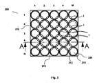
- each electrode element 210 is part of an individual column of the plurality of columns, which are, in correspondence to their electrode elements, arranged in the 5 x 5 array.
- the array of electrode elements 210 is a regular rectangular array having rows 1 to N, in this case rows 1 to 5 and lines 1 to M, herein lines 1 to 5.
- each electrode element 210 has an aperture 213 having a noncircular shape.
- Each aperture 213 is formed by inner peripheral edge 212 of electrode element 210. Inner edges of cylindrical outer members 220 are also visible in Figure 3 .
- the non-circular shapes comprise at least one indentation I from an ideal circular shape.
- the shapes of the apertures 213 are dependent on a position of the respective electrode element 210 within the array 250.
- the apertures 213 of electrode elements 210 of a first group of columns) disposed in positions (row, line) (1,1), (N, 1), (1, M) and (N, M) have a shape with one indentation I each, the respective indentation I facing away from a respective corner of the array.
- the apertures 213 of electrode elements 210 of a second group of columns disposed in positions (row, line)(2-4, 1), (1, 2-4), (2-4, M) and (N, 2-4) have substantially the same non-circular shape (excluding the orientation thereof) having two indentations I from an ideal circular shape each.
- the apertures 213 of electrode elements 210 of a third group of columns disposed in positions (row, line) (2-4, 2-4) have substantially a same shape with four indentations I from an ideal circular shape.
- the difference between the apertures of the respective groups is the number of nearest and second nearest neighbours and the symmetry of the configuration of neighbouring columns.
- the apertures of the first group of columns are disposed on corners of the array and have two nearest and one second nearest neighbour.
- Electrostatic fields generated by such an environment may be compensated for by the provision of one indentation oriented in a direction of the second nearest neighbouring column.
- the columns disposed on edges of the array, but not on corners have neighbouring columns in three directions with three nearest and two second nearest neighbouring columns each.
- Electrostatic fields generated by such an environment may be suitably compensated four by providing the respective apertures 213 with a non-circular shape having two indentations I from an ideal circular shape, with the indentations I being oriented in directions of the second nearest neighbouring columns.
- a column of the third group is disposed inside the array, i.e. is surrounded by neighbouring columns in all four directions.
- an electrode element 210X inside a regular, rectangular array 250 is surrounded by a first sphere 1SP of nearest neighbouring columns, the first sphere being marked by a dashed line running through centres of the four nearest electrode elements 210-1SP around electrode element 210X, which are indicated by a hatch pattern.
- Electrode elements 210-2SP disposed second nearest to electrode element 210X are indicated by a square pattern, the second sphere 2SP being further indicated by dotted line 2SP running through centres of the second nearest electrode elements 210-2SP.
- a third sphere is further indicated by dashed line 3SP.
- the aperture 213 is an aperture 213 of an electrode element 210 of a column of the third group of columns, as described above.
- the non-circular shape, in particular a deviation of the shape of the aperture 213 from an ideal circle is characterised herein by a difference between a distance D1 from the centre of the aperture 213, which typically coincides with the optical axis, and a point on the inner peripheral edge 212 forming the aperture 213, which point is disclosed closest to the optical axis, i.e. is a shortest distance of any point on the inner peripheral edge 212 from the centre of the aperture 213.
- the centre of the aperture is marked by a black dot.
- a second distance D2 is defined as the distance of a point on the inner peripheral edge 212 that is disposed farthest from the centre of the aperture 213.
- the indentation I is a shape feature describing a portion of the aperture, which deviates from an ideal spherical shape and extends towards the centre of the aperture 213.
- An ideal spherical shape IC may be defined to be a circle with a centre coinciding with the centre of the aperture and having a radius equal to the second distance D2. This definition was chosen for sake of simplicity. As will be readily apparent to the skilled person, other definitions may have been chosen to describe a non-circular shape.
- Inner peripheral edge of outer ring member 220 is also depicted, with the same considerations as given in connection with Figure 3 applying.
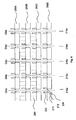
- Array 250 is one of a plurality of arrays 250A through 250D which are arranged in series along the optical axes OA (a through e) of the individual columns a through e and parallel to one another in a plane orthogonal to the optical axes OAa through OAe.
- Each column a, b, c, d, e has an electrostatic lens arrangement with a plurality of electrode elements 210a, 210b, 210c, 210d, 210e, respectively, disposed coaxially one after another in a stack along a respective optical axis OAa, OAb, OAc, OAd, OAe of the column a, b, c, d, e.
- Each electrode element 210 a through e comprises an inner electrode member 211 around the respective optical axis OA.
- Each electrode element 210 a through e further comprises a shielding member 222 of cylindrical shape disposed in a region of an outer periphery of inner electrode member 211 and on plate 230.
- Shielding member is disposed in a gap between two adjacent arrays 250A/, B/C, C/D, D/E in order to prevent electrostatic fields from penetrating inside the respective electrostatic lens formed by respective electrode elements.
- Plate 230 may be a mounting structure in the form of a plate comprising apertures for accommodating inner electrode members.
- inner electrode member 211 and shielding member 222 may be attached to plate 230 independently, with the inner electrode member 211 being inserted into a respective aperture of the mounting plate whereas cylindrical shielding member is disposed around a circumference of the respective aperture.
- plate 230 may be a portion of the electrode element 210 comprising outer ring portion 220 as well as connector 221 as depicted in Figure 2 , with respective portions 230 of neighbouring electrode elements 210 a through e (in the same plane orthogonal to the optical axis) being connected to one another.
- the electrode elements 210 and plate 230 may be integrally formed, for instance.
- Figure 6 illustrates the coaxial alignment of the electrode members 211 (a through e, respectively) disposed in series along the optical axis and configuration of electrode elements 210 of neighbouring columns on a common mounting structure.
- a few insulating spacer elements 280 arranged between mounting plates 250A/B and B/C to space them apart are also illustrated as an example.
- spacer elements could also be disposed between the other mounting structures (not depicted for ease of illustration).
- fewer spacer elements could be used in between two given mounting plates, or they could be disposed in different positions relative to the apertures and the like, as will be readily apparent to the skilled person.
Landscapes
- Engineering & Computer Science (AREA)
- Chemical & Material Sciences (AREA)
- Nanotechnology (AREA)
- Physics & Mathematics (AREA)
- Crystallography & Structural Chemistry (AREA)
- Analytical Chemistry (AREA)
- Condensed Matter Physics & Semiconductors (AREA)
- General Physics & Mathematics (AREA)
- Manufacturing & Machinery (AREA)
- Mathematical Physics (AREA)
- Theoretical Computer Science (AREA)
- Electron Beam Exposure (AREA)
Claims (24)
- Multistrahlen-, Multisäulen- teilchenoptisches System, umfassend eine Vielzahl von teilchenoptischen Multistrahlen-Säulen (1),
wobei die Vielzahl von teilchenoptischen Multistrahlen-Säulen in einem Array angeordnet ist, um gleichzeitig dasselbe Substrat (5) zu bestrahlen,
wobei jede teilchenoptische Säule eine optische Achse (0A) aufweist und Folgendes umfasst:eine Teilstrahlen generierende Anordnung (100), die mindestens eine Multiaperturblende (140) umfasst, die eine Vielzahl von Aperturen aufweist, um ein Muster aus mehreren Teilstrahlen geladener Teilchen zu generieren, undeine elektrostatische Linsenanordnung (200) stromabwärts der Teilstrahlen generierenden Anordnung, wobei die elektrostatische Linsenanordnung mindestens ein Elektrodenelement (210) umfasst,wobei das mindestens eine Elektrodenelement eine Apertur (213) aufweist, welche die generierten mehreren Teilstrahlen von geladenen Teilchen durchtreten lässt, wobei die Apertur durch einen inneren umlaufenden Rand (212) definiert ist, welcher der optischen Achse zugewandt ist, wobei die Apertur ein Zentrum und eine vorbestimmte Form in einer Ebene (P) aufweist, die zur optischen Achse orthogonal ist;wobei in mindestens einer der Vielzahl von geladenen Teilchensäulen die vorbestimmte Form der Apertur des mindestens einen Elektrodenelements eine unkreisförmige Form mit mindestens einem Vorsprung oder einer Einbuchtung (I) im Verhältnis zu einem idealen Kreis (IC) um das Zentrum der Apertur herum ist, undwobei ein erster Abstand (D1) zwischen einem Punkt auf dem inneren umlaufenden Rand der Apertur, der am nächsten am Zentrum der Apertur angeordnet ist, um mindestens ungefähr 5 % kleiner ist als ein zweiter Abstand (D2) zwischen einem Punkt auf dem inneren umlaufenden Rand der Apertur, der am weitesten vom Zentrum der Apertur entfernt angeordnet ist. - Teilchenoptisches System gemäß Anspruch 1, wobei das Elektrodenelement ein ringförmiges Innenelektrodenbauteil umfasst, das einen inneren umlaufenden Rand aufweist, und wobei die Apertur durch den inneren umlaufenden Rand gebildet ist.
- Teilchenoptisches System gemäß Anspruch 1, wobei die elektrostatische Linsenanordnung der mindestens einen Säule der Vielzahl von Säulen mit mehreren Teilstrahlen von geladenen Teilchen zwei oder mehrere Elektrodenelemente umfasst, die koaxial und in der Richtung der optischen Achse beabstandet angeordnet sind.
- Teilchenoptisches System gemäß Anspruch 3, wobei die Aperturen der mindestens zwei Elektrodenelemente im Wesentlichen die gleiche unkreisförmige Form aufweisen.
- Teilchenoptisches System gemäß Anspruch 4, wobei die Apertur eines ersten Elektrodenelements der mindestens zwei Elektrodenelemente einen Bereich aufweist, der um mindestens 5 % größer ist als eine Fläche der Apertur eines zweiten Elektrodenelements der mindestens zwei Elektrodenelemente.
- Teilchenoptisches System gemäß Anspruch 1, wobei die Vielzahl von Säulen eine erste Gruppe von Säulen umfasst, die mindestens eine Säule umfasst, wobei die Apertur des mindestens einen Elektrodenelements der elektrostatischen Anordnung jeder Säule der ersten Gruppe von Säulen eine erste Form aufweist, und ferner umfassend eine zweite Gruppe von Säulen, die mindestens eine Säule umfasst, wobei die Apertur des mindestens einen Elektrodenelements der elektrostatischen Anordnung jeder Säule der zweiten Gruppe von Säulen eine zweite Form aufweist, die anders als die erste Form ist.
- Teilchenoptisches System gemäß Anspruch 6, wobei die erste Form anders als die zweite Form im Verhältnis zu mindestens einem Element aus einer gewissen Anzahl von Einbuchtungen, einer gewissen Anzahl von Vorsprüngen, einer Form eines Vorsprungs, einer Form einer Einbuchtung, einer Größe eines Vorsprungs, einer Größe einer Einbuchtung, einer Symmetrie der Form und einer beliebigen Kombination davon ist.
- Teilchenoptisches System gemäß Anspruch 6, wobei jede Säule der ersten Gruppe von Säulen von einer ersten Konfiguration von benachbarten Säulen umgeben ist und jede Säule der zweiten Gruppe von Säulen von einer zweiten Konfiguration von benachbarten Säulen umgeben ist, und wobei die erste Konfiguration anders als die zweite Konfiguration ist.
- Teilchenoptisches System gemäß Anspruch 8, wobei die erste Konfiguration anders als die zweite Konfiguration im Verhältnis zu mindestens einem Element aus einer gewissen Anzahl von benachbarten Säulen, die am nächsten an der jeweiligen Säule angeordnet sind, einer gewissen Anzahl von benachbarten Säulen, die am zweitnächsten an der jeweiligen Säule angeordnet sind, einer Symmetrie der Konfiguration der benachbarten Säulen und einer beliebigen Kombination davon ist.
- Teilchenoptisches System gemäß Anspruch 1, wobei die unkreisförmige Form eine Form umfasst, die eine, zwei oder vier Einbuchtungen umfasst, die sich von einem idealen Kreis aus in Richtung auf das Zentrum der Apertur hin erstrecken, wobei der ideale Kreis einen Radius aufweist, der gleich dem zweiten Abstand ist.
- Teilchenoptisches System gemäß Anspruch 1, wobei jede Säule mindestens eine nächstgelegene benachbarte und mindestens eine zweitnächstgelegene benachbarte Säule aufweist, und wobei eine Anzahl von Einbuchtungen in der Form der Apertur des mindestens einen Elektrodenelements der mindestens einen Säule gleich einer Anzahl von zweitnächsten Säulen um die mindestens eine Säule herum ist, wobei sich die Einbuchtungen von dem idealen Kreis aus in Richtung auf das Zentrum der Apertur hin erstrecken, wobei der ideale Kreis einen Radius aufweist, der gleich dem zweiten Abstand ist.
- Teilchenoptisches System gemäß Anspruch 6,
wobei die teilchenoptischen Multistrahlen-Säulen in einem rechteckigen Array aus N Reihen 1 bis N und M Spalten 1 bis M, die zu den Reihen orthogonal sind, angeordnet sind,
wobei eine dritte Gruppe von Säulen aus Säulen besteht, die in Spalte 1, Reihe 2 bis N-1, und Spalte M, Reihe 2 bis N-1, und in Reihe 1, Spalten 2 bis M-1 und Reihe N, Spalten 2 bis N-1, angeordnet sind, und wobei die Aperturen des mindestens einen Elektrodenelements der elektrostatischen Anordnung jeder Säule der dritten Gruppe von Säulen eine gleiche dritte Form aufweisen. - Teilchenoptisches System gemäß Anspruch 12,
wobei die teilchenoptischen Multistrahlen-Säulen in einem rechteckigen Array aus N Reihen 1 bis N und M Spalten 1 bis M, die zu den Reihen orthogonal sind, angeordnet sind,
wobei eine vierte Gruppe von Säulen aus Säulen besteht, die in Spalte 1, Reihe 1, in Spalte 1, Reihe N, in Spalte M, Reihe 1, und in Spalte M, Reihe N, angeordnet sind,
und wobei die Aperturen des mindestens einen Elektrodenelements der elektrostatischen Anordnung jeder Säule der vierten Gruppe von Säulen eine gleiche vierte Form aufweisen. - Teilchenoptisches System gemäß Anspruch 13, wobei die teilchenoptischen Multistrahlen-Säulen in einem rechteckigen Array aus N Reihen 1 bis N und M Spalten 1 bis M, die zu den Reihen orthogonal sind, angeordnet sind,
wobei eine fünfte Gruppe von Säulen aus Säulen besteht, die in Spalte 2 bis M-1 in jeweiligen Reihen 2 bis N-1 angeordnet sind,
und wobei die Aperturen des mindestens einen Elektrodenelements der elektrostatischen Anordnung jeder Säule der fünften Gruppe von Säulen eine gleiche fünfte Form aufweisen. - Teilchenoptisches System gemäß Anspruch 1, wobei das mindestens eine Elektrodenelement der elektrostatischen Anordnungen aus benachbarten Säulen den gleichen Abstand von einer Substratebene aufweisen und auf einer Befestigungsvorrichtung (270) angeordnet sind, die sich im Wesentlichen in einer Ebene erstreckt, die zu den optischen Achsen der benachbarten Säulen orthogonal ist.
- Teilchenoptisches System gemäß Anspruch 1, ferner umfassend eine erste und zweite Befestigungsvorrichtung,
wobei die optischen Achsen von Säulen, die nebeneinander angeordnet sind, parallel angeordnet sind,
wobei jede der benachbarten Säulen zwei oder mehrere Elektrodenelemente umfasst, wobei ein erstes Elektrodenelement und mindestens ein zweites Elektrodenelement koaxial und in der Richtung der optischen Achse der Säule beabstandet angeordnet sind,
wobei die ersten Elektrodenelemente der benachbarten Säulen einen gleichen ersten Abstand von einer Substratebene aufweisen und auf der ersten Befestigungsvorrichtung angeordnet sind,
wobei die zweiten Elektrodenelemente der benachbarten Säulen einen gleichen zweiten Abstand von der Substratebene aufweisen und auf der zweiten Befestigungsvorrichtung angeordnet sind, wobei die ersten und zweiten Befestigungsvorrichtungen in einer Ebene, die zu den optischen Achsen der Säulen orthogonal ist, parallel zueinander angeordnet sind. - Teilchenoptisches System gemäß Anspruch 16, wobei die ersten und zweiten Befestigungsvorrichtungen durch elektrisch isolierende Distanzstücke beabstandet sind.
- Teilchenoptisches System gemäß Anspruch 3, wobei die Elektrodenelemente ferner ein im Wesentlichen zylindrisches Abschirmelement (222) umfassen, wobei das im Wesentlichen zylindrische Abschirmelement einen Radius aufweist, der gleich oder größer als der zweite Abstand ist.
- Teilchenoptisches System gemäß Anspruch 1, wobei die Öffnung derart geformt und angeordnet ist, dass sie eine Mehrpol-Korrektur für elektrostatische Felder bereitstellt, die in der Elektrodenanordnung generiert werden.
- Teilchenoptisches System gemäß Anspruch 1, wobei die Teilstrahlen generierende Anordnung eine Quelle für geladene Teilchen (110), um einen Strahl von geladenen Teilchen zu generieren, und eine Einrichtung zur Strahlanordnung stromabwärts von der geladenen Teilchenquelle umfasst, wobei die Einrichtung zur Strahlanordnung mindestens die Multiaperturblende umfasst und konfiguriert ist, um mindestens einen Teil des geladenen Teilchenstrahls zu unterdrücken, so dass ein Muster aus mehreren Teilstrahlen stromabwärts von der Musterstruktur gebildet wird.
- Teilchenoptisches System gemäß Anspruch 1, wobei das Zentrum der mindestens einen Apertur des Elektrodenelements der elektrostatischen Linsenanordnung einer ersten Säule mindestens 50 mm vom Zentrum der mindestens einen Apertur des Elektrodenelements der elektrostatischen Linsenanordnung einer zweiten Säule angeordnet ist, wobei die zweite Säule am nächsten an der ersten Säule in dem Array aus Multistrahlen- geladenen Teilchensäulen angeordnet ist.
- Teilchenoptisches System gemäß Anspruch 1, wobei die Form der Apertur im Verhältnis zur optischen Achse der jeweiligen Mehrstrahlen- teilchenoptischen Säule asymmetrisch ist.
- Teilchenoptisches System gemäß Anspruch 1, wobei das Zentrum der Apertur auf der optischen Achse der jeweiligen Multistrahlen- teilchenoptischen Säule angeordnet ist.
- Verfahren zum Bestrahlen eines Substrats durch Mehrstrahlen-, Multisäulenbelichtung, umfassend folgende Schritte:Generieren einer Vielzahl von mehreren Teilstrahlmustern durch eine jeweilige Vielzahl von Multistrahlenteilchenoptischen Säulen des teilchenoptischen Systems gemäß Anspruch 1 und Richten der Vielzahl von mehreren Teilstrahlmustern auf ein zu bestrahlendes Substrat;Generieren von elektrostatischen Feldern durch Anlegen elektrischer Potenziale an mindestens ein Elektrodenelement der elektrostatischen Linsenanordnungen der Vielzahl von Multistrahlen- teilchenoptischen Säulen;Übertragen jeweils einer der mehreren Teilstrahlmuster durch jeweils eine der jeweilige Aperturen der Elektrodenelemente der elektrostatischen Linsenanordnungen der Vielzahl von Multistrahlen- teilchenoptischen Säulen.
Priority Applications (4)
| Application Number | Priority Date | Filing Date | Title |
|---|---|---|---|
| EP05017318A EP1753010B1 (de) | 2005-08-09 | 2005-08-09 | Teilchenoptisches System |
| US11/990,067 US8368015B2 (en) | 2005-08-09 | 2006-08-08 | Particle-optical system |
| PCT/EP2006/007849 WO2007017255A1 (en) | 2005-08-09 | 2006-08-08 | Particle-optical system |
| JP2008525473A JP5243249B2 (ja) | 2005-08-09 | 2006-08-08 | 粒子光学系 |
Applications Claiming Priority (1)
| Application Number | Priority Date | Filing Date | Title |
|---|---|---|---|
| EP05017318A EP1753010B1 (de) | 2005-08-09 | 2005-08-09 | Teilchenoptisches System |
Publications (2)
| Publication Number | Publication Date |
|---|---|
| EP1753010A1 EP1753010A1 (de) | 2007-02-14 |
| EP1753010B1 true EP1753010B1 (de) | 2012-12-05 |
Family
ID=36061724
Family Applications (1)
| Application Number | Title | Priority Date | Filing Date |
|---|---|---|---|
| EP05017318A Expired - Lifetime EP1753010B1 (de) | 2005-08-09 | 2005-08-09 | Teilchenoptisches System |
Country Status (4)
| Country | Link |
|---|---|
| US (1) | US8368015B2 (de) |
| EP (1) | EP1753010B1 (de) |
| JP (1) | JP5243249B2 (de) |
| WO (1) | WO2007017255A1 (de) |
Families Citing this family (17)
| Publication number | Priority date | Publication date | Assignee | Title |
|---|---|---|---|---|
| JP2008066359A (ja) * | 2006-09-05 | 2008-03-21 | Canon Inc | 荷電ビームレンズアレイ、露光装置及びデバイス製造方法 |
| KR101570974B1 (ko) | 2008-02-26 | 2015-11-23 | 마퍼 리쏘그라피 아이피 비.브이. | 투사 렌즈 배열체 |
| KR101420244B1 (ko) | 2008-05-20 | 2014-07-21 | 재단법인서울대학교산학협력재단 | 전자빔 집속 전극 및 이를 이용한 전자총 |
| US10586625B2 (en) | 2012-05-14 | 2020-03-10 | Asml Netherlands B.V. | Vacuum chamber arrangement for charged particle beam generator |
| NL2013814B1 (en) | 2013-11-14 | 2016-05-10 | Mapper Lithography Ip Bv | Multi-electrode vacuum arrangement. |
| JP6257411B2 (ja) * | 2014-03-27 | 2018-01-10 | 住友重機械イオンテクノロジー株式会社 | イオン注入装置、最終エネルギーフィルター、及びイオン注入方法 |
| CN107710383A (zh) | 2015-06-08 | 2018-02-16 | 株式会社尼康 | 带电粒子束曝光装置及器件制造方法 |
| WO2018074306A1 (ja) | 2016-10-17 | 2018-04-26 | 株式会社ニコン | 露光システム及びリソグラフィシステム |
| US10453645B2 (en) * | 2016-12-01 | 2019-10-22 | Applied Materials Israel Ltd. | Method for inspecting a specimen and charged particle multi-beam device |
| JP6720861B2 (ja) * | 2016-12-28 | 2020-07-08 | 株式会社ニューフレアテクノロジー | マルチビーム用アパーチャセット及びマルチ荷電粒子ビーム描画装置 |
| US10347460B2 (en) | 2017-03-01 | 2019-07-09 | Dongfang Jingyuan Electron Limited | Patterned substrate imaging using multiple electron beams |
| KR102649183B1 (ko) * | 2017-10-02 | 2024-03-21 | 에이에스엠엘 네델란즈 비.브이. | 하전 입자 빔들을 사용하는 장치 |
| WO2019211072A1 (en) | 2018-05-01 | 2019-11-07 | Asml Netherlands B.V. | Multi-beam inspection apparatus |
| DE102018007652B4 (de) | 2018-09-27 | 2021-03-25 | Carl Zeiss Multisem Gmbh | Teilchenstrahl-System sowie Verfahren zur Stromregulierung von Einzel-Teilchenstrahlen |
| WO2020141031A1 (en) | 2018-12-31 | 2020-07-09 | Asml Netherlands B.V. | Multi-beam inspection apparatus |
| EP3703100A1 (de) * | 2019-02-27 | 2020-09-02 | FEI Company | Ladungsteilchenstrahlvorrichtung zur inspektion einer probe mit einer vielzahl von ladungsteilchenteilstrahlen |
| US11899375B2 (en) | 2020-11-20 | 2024-02-13 | Kla Corporation | Massive overlay metrology sampling with multiple measurement columns |
Family Cites Families (22)
| Publication number | Priority date | Publication date | Assignee | Title |
|---|---|---|---|---|
| JPS6066816A (ja) * | 1983-09-22 | 1985-04-17 | Fujitsu Ltd | 電子ビ−ム露光装置 |
| US5369282A (en) | 1992-08-03 | 1994-11-29 | Fujitsu Limited | Electron beam exposure method and system for exposing a pattern on a substrate with an improved accuracy and throughput |
| JP3206143B2 (ja) | 1992-10-20 | 2001-09-04 | 富士通株式会社 | 荷電粒子ビーム露光方法 |
| JP3647128B2 (ja) * | 1996-03-04 | 2005-05-11 | キヤノン株式会社 | 電子ビーム露光装置とその露光方法 |
| JPH11150050A (ja) * | 1997-11-17 | 1999-06-02 | Nec Corp | 電子線描画装置及び描画方法 |
| WO2001039243A1 (en) * | 1999-11-23 | 2001-05-31 | Ion Diagnostics, Inc. | Electron optics for multi-beam electron beam lithography tool |
| JP2001284230A (ja) | 2000-03-31 | 2001-10-12 | Canon Inc | 電子光学系アレイ、これを用いた荷電粒子線露光装置ならびにデバイス製造方法 |
| JP4585661B2 (ja) | 2000-03-31 | 2010-11-24 | キヤノン株式会社 | 電子光学系アレイ、荷電粒子線露光装置およびデバイス製造方法 |
| JP4601146B2 (ja) | 2000-10-03 | 2010-12-22 | 株式会社アドバンテスト | 電子ビーム露光装置 |
| JP2002217089A (ja) | 2001-01-18 | 2002-08-02 | Advantest Corp | 電子ビーム偏向装置、電子ビーム偏向装置の製造方法、及び電子ビーム露光装置 |
| US6768125B2 (en) | 2002-01-17 | 2004-07-27 | Ims Nanofabrication, Gmbh | Maskless particle-beam system for exposing a pattern on a substrate |
| US7041988B2 (en) * | 2002-05-10 | 2006-05-09 | Advantest Corp. | Electron beam exposure apparatus and electron beam processing apparatus |
| JP2003332204A (ja) * | 2002-05-10 | 2003-11-21 | Advantest Corp | 露光装置、及び電子銃 |
| JP2003331772A (ja) * | 2002-05-16 | 2003-11-21 | Ebara Corp | 電子線装置及びデバイス製造方法 |
| JP2003346698A (ja) * | 2002-05-30 | 2003-12-05 | Ebara Corp | 電子線装置及びデバイス製造方法 |
| JP4180854B2 (ja) * | 2002-07-16 | 2008-11-12 | キヤノン株式会社 | 電子ビーム描画装置 |
| JP2004165076A (ja) * | 2002-11-15 | 2004-06-10 | Advantest Corp | 偏向器の製造方法、偏向器、及び露光装置 |
| CN102709143B (zh) * | 2003-09-05 | 2016-03-09 | 卡尔蔡司Smt有限责任公司 | 电子光学排布结构、多电子分束检验系统和方法 |
| GB2406704B (en) | 2003-09-30 | 2007-02-07 | Ims Nanofabrication Gmbh | Particle-optic electrostatic lens |
| GB2408143B (en) | 2003-10-20 | 2006-11-15 | Ims Nanofabrication Gmbh | Charged-particle multi-beam exposure apparatus |
| JP3913250B2 (ja) | 2005-01-07 | 2007-05-09 | キヤノン株式会社 | 電子ビーム露光装置とその露光方法 |
| JP4745739B2 (ja) | 2005-07-06 | 2011-08-10 | キヤノン株式会社 | 静電レンズ装置、露光装置、及びデバイス製造方法 |
-
2005
- 2005-08-09 EP EP05017318A patent/EP1753010B1/de not_active Expired - Lifetime
-
2006
- 2006-08-08 JP JP2008525473A patent/JP5243249B2/ja not_active Expired - Fee Related
- 2006-08-08 WO PCT/EP2006/007849 patent/WO2007017255A1/en not_active Ceased
- 2006-08-08 US US11/990,067 patent/US8368015B2/en not_active Expired - Fee Related
Also Published As
| Publication number | Publication date |
|---|---|
| US8368015B2 (en) | 2013-02-05 |
| WO2007017255A1 (en) | 2007-02-15 |
| US20100270474A1 (en) | 2010-10-28 |
| JP5243249B2 (ja) | 2013-07-24 |
| EP1753010A1 (de) | 2007-02-14 |
| JP2009505384A (ja) | 2009-02-05 |
Similar Documents
| Publication | Publication Date | Title |
|---|---|---|
| EP1753010B1 (de) | Teilchenoptisches System | |
| EP1668662B1 (de) | Optische partikelsysteme und anordnungen und optische partikelkomponenten für solche systeme und anordnungen | |
| KR101900050B1 (ko) | 멀티 하전 입자빔 장치 | |
| US9620329B1 (en) | Electrostatic multipole device, electrostatic multipole arrangement, charged particle beam device, and method of manufacturing an electrostatic multipole device | |
| EP2339608B1 (de) | Elektrostatischer Korrektor | |
| US9620328B1 (en) | Electrostatic multipole device, electrostatic multipole arrangement, charged particle beam device, and method of operating an electrostatic multipole device | |
| WO2012124320A1 (en) | Charged particle beam lens and exposure apparatus using the same |
Legal Events
| Date | Code | Title | Description |
|---|---|---|---|
| PUAI | Public reference made under article 153(3) epc to a published international application that has entered the european phase |
Free format text: ORIGINAL CODE: 0009012 |
|
| AK | Designated contracting states |
Kind code of ref document: A1 Designated state(s): AT BE BG CH CY CZ DE DK EE ES FI FR GB GR HU IE IS IT LI LT LU LV MC NL PL PT RO SE SI SK TR |
|
| AX | Request for extension of the european patent |
Extension state: AL BA HR MK YU |
|
| RIN1 | Information on inventor provided before grant (corrected) |
Inventor name: PLATZGUMMER, ELMAR, DR. DIPL.-ING. Inventor name: STENGL, GERHARD, DR. DIPL.-ING. Inventor name: FALKNER, HELMUT |
|
| 17P | Request for examination filed |
Effective date: 20070808 |
|
| AKX | Designation fees paid |
Designated state(s): AT BE BG CH CY CZ DE DK EE ES FI FR GB GR HU IE IS IT LI LT LU LV MC NL PL PT RO SE SI SK TR |
|
| GRAP | Despatch of communication of intention to grant a patent |
Free format text: ORIGINAL CODE: EPIDOSNIGR1 |
|
| RIC1 | Information provided on ipc code assigned before grant |
Ipc: H01J 37/317 20060101AFI20111222BHEP Ipc: H01J 37/12 20060101ALI20111222BHEP Ipc: B82Y 10/00 20110101ALI20111222BHEP |
|
| GRAS | Grant fee paid |
Free format text: ORIGINAL CODE: EPIDOSNIGR3 |
|
| GRAA | (expected) grant |
Free format text: ORIGINAL CODE: 0009210 |
|
| AK | Designated contracting states |
Kind code of ref document: B1 Designated state(s): AT BE BG CH CY CZ DE DK EE ES FI FR GB GR HU IE IS IT LI LT LU LV MC NL PL PT RO SE SI SK TR |
|
| REG | Reference to a national code |
Ref country code: GB Ref legal event code: FG4D Ref country code: DE Ref legal event code: R081 Ref document number: 602005037253 Country of ref document: DE Owner name: CARL ZEISS SMT GMBH, DE Free format text: FORMER OWNER: CARL ZEISS SMS GMBH, 07745 JENA, DE |
|
| REG | Reference to a national code |
Ref country code: CH Ref legal event code: EP |
|
| REG | Reference to a national code |
Ref country code: AT Ref legal event code: REF Ref document number: 587662 Country of ref document: AT Kind code of ref document: T Effective date: 20121215 |
|
| REG | Reference to a national code |
Ref country code: IE Ref legal event code: FG4D |
|
| REG | Reference to a national code |
Ref country code: DE Ref legal event code: R096 Ref document number: 602005037253 Country of ref document: DE Effective date: 20130131 |
|
| REG | Reference to a national code |
Ref country code: NL Ref legal event code: T3 |
|
| PG25 | Lapsed in a contracting state [announced via postgrant information from national office to epo] |
Ref country code: FI Free format text: LAPSE BECAUSE OF FAILURE TO SUBMIT A TRANSLATION OF THE DESCRIPTION OR TO PAY THE FEE WITHIN THE PRESCRIBED TIME-LIMIT Effective date: 20121205 Ref country code: ES Free format text: LAPSE BECAUSE OF FAILURE TO SUBMIT A TRANSLATION OF THE DESCRIPTION OR TO PAY THE FEE WITHIN THE PRESCRIBED TIME-LIMIT Effective date: 20130316 Ref country code: LT Free format text: LAPSE BECAUSE OF FAILURE TO SUBMIT A TRANSLATION OF THE DESCRIPTION OR TO PAY THE FEE WITHIN THE PRESCRIBED TIME-LIMIT Effective date: 20121205 Ref country code: SE Free format text: LAPSE BECAUSE OF FAILURE TO SUBMIT A TRANSLATION OF THE DESCRIPTION OR TO PAY THE FEE WITHIN THE PRESCRIBED TIME-LIMIT Effective date: 20121205 |
|
| REG | Reference to a national code |
Ref country code: LT Ref legal event code: MG4D |
|
| PG25 | Lapsed in a contracting state [announced via postgrant information from national office to epo] |
Ref country code: PL Free format text: LAPSE BECAUSE OF FAILURE TO SUBMIT A TRANSLATION OF THE DESCRIPTION OR TO PAY THE FEE WITHIN THE PRESCRIBED TIME-LIMIT Effective date: 20121205 Ref country code: SI Free format text: LAPSE BECAUSE OF FAILURE TO SUBMIT A TRANSLATION OF THE DESCRIPTION OR TO PAY THE FEE WITHIN THE PRESCRIBED TIME-LIMIT Effective date: 20121205 Ref country code: CY Free format text: LAPSE BECAUSE OF FAILURE TO SUBMIT A TRANSLATION OF THE DESCRIPTION OR TO PAY THE FEE WITHIN THE PRESCRIBED TIME-LIMIT Effective date: 20121205 Ref country code: LV Free format text: LAPSE BECAUSE OF FAILURE TO SUBMIT A TRANSLATION OF THE DESCRIPTION OR TO PAY THE FEE WITHIN THE PRESCRIBED TIME-LIMIT Effective date: 20121205 Ref country code: GR Free format text: LAPSE BECAUSE OF FAILURE TO SUBMIT A TRANSLATION OF THE DESCRIPTION OR TO PAY THE FEE WITHIN THE PRESCRIBED TIME-LIMIT Effective date: 20130306 |
|
| PG25 | Lapsed in a contracting state [announced via postgrant information from national office to epo] |
Ref country code: EE Free format text: LAPSE BECAUSE OF FAILURE TO SUBMIT A TRANSLATION OF THE DESCRIPTION OR TO PAY THE FEE WITHIN THE PRESCRIBED TIME-LIMIT Effective date: 20121205 Ref country code: IS Free format text: LAPSE BECAUSE OF FAILURE TO SUBMIT A TRANSLATION OF THE DESCRIPTION OR TO PAY THE FEE WITHIN THE PRESCRIBED TIME-LIMIT Effective date: 20130405 Ref country code: CZ Free format text: LAPSE BECAUSE OF FAILURE TO SUBMIT A TRANSLATION OF THE DESCRIPTION OR TO PAY THE FEE WITHIN THE PRESCRIBED TIME-LIMIT Effective date: 20121205 Ref country code: BE Free format text: LAPSE BECAUSE OF FAILURE TO SUBMIT A TRANSLATION OF THE DESCRIPTION OR TO PAY THE FEE WITHIN THE PRESCRIBED TIME-LIMIT Effective date: 20121205 Ref country code: SK Free format text: LAPSE BECAUSE OF FAILURE TO SUBMIT A TRANSLATION OF THE DESCRIPTION OR TO PAY THE FEE WITHIN THE PRESCRIBED TIME-LIMIT Effective date: 20121205 Ref country code: BG Free format text: LAPSE BECAUSE OF FAILURE TO SUBMIT A TRANSLATION OF THE DESCRIPTION OR TO PAY THE FEE WITHIN THE PRESCRIBED TIME-LIMIT Effective date: 20130305 |
|
| PG25 | Lapsed in a contracting state [announced via postgrant information from national office to epo] |
Ref country code: PT Free format text: LAPSE BECAUSE OF FAILURE TO SUBMIT A TRANSLATION OF THE DESCRIPTION OR TO PAY THE FEE WITHIN THE PRESCRIBED TIME-LIMIT Effective date: 20130405 Ref country code: RO Free format text: LAPSE BECAUSE OF FAILURE TO SUBMIT A TRANSLATION OF THE DESCRIPTION OR TO PAY THE FEE WITHIN THE PRESCRIBED TIME-LIMIT Effective date: 20121205 |
|
| PLBE | No opposition filed within time limit |
Free format text: ORIGINAL CODE: 0009261 |
|
| STAA | Information on the status of an ep patent application or granted ep patent |
Free format text: STATUS: NO OPPOSITION FILED WITHIN TIME LIMIT |
|
| PG25 | Lapsed in a contracting state [announced via postgrant information from national office to epo] |
Ref country code: DK Free format text: LAPSE BECAUSE OF FAILURE TO SUBMIT A TRANSLATION OF THE DESCRIPTION OR TO PAY THE FEE WITHIN THE PRESCRIBED TIME-LIMIT Effective date: 20121205 |
|
| 26N | No opposition filed |
Effective date: 20130906 |
|
| PG25 | Lapsed in a contracting state [announced via postgrant information from national office to epo] |
Ref country code: IT Free format text: LAPSE BECAUSE OF FAILURE TO SUBMIT A TRANSLATION OF THE DESCRIPTION OR TO PAY THE FEE WITHIN THE PRESCRIBED TIME-LIMIT Effective date: 20121205 |
|
| REG | Reference to a national code |
Ref country code: DE Ref legal event code: R097 Ref document number: 602005037253 Country of ref document: DE Effective date: 20130906 |
|
| REG | Reference to a national code |
Ref country code: CH Ref legal event code: PL |
|
| GBPC | Gb: european patent ceased through non-payment of renewal fee |
Effective date: 20130809 |
|
| PG25 | Lapsed in a contracting state [announced via postgrant information from national office to epo] |
Ref country code: MC Free format text: LAPSE BECAUSE OF FAILURE TO SUBMIT A TRANSLATION OF THE DESCRIPTION OR TO PAY THE FEE WITHIN THE PRESCRIBED TIME-LIMIT Effective date: 20121205 Ref country code: LI Free format text: LAPSE BECAUSE OF NON-PAYMENT OF DUE FEES Effective date: 20130831 Ref country code: CH Free format text: LAPSE BECAUSE OF NON-PAYMENT OF DUE FEES Effective date: 20130831 |
|
| REG | Reference to a national code |
Ref country code: IE Ref legal event code: MM4A |
|
| REG | Reference to a national code |
Ref country code: FR Ref legal event code: ST Effective date: 20140430 |
|
| PG25 | Lapsed in a contracting state [announced via postgrant information from national office to epo] |
Ref country code: IE Free format text: LAPSE BECAUSE OF NON-PAYMENT OF DUE FEES Effective date: 20130809 Ref country code: GB Free format text: LAPSE BECAUSE OF NON-PAYMENT OF DUE FEES Effective date: 20130809 |
|
| PG25 | Lapsed in a contracting state [announced via postgrant information from national office to epo] |
Ref country code: FR Free format text: LAPSE BECAUSE OF NON-PAYMENT OF DUE FEES Effective date: 20130902 |
|
| PG25 | Lapsed in a contracting state [announced via postgrant information from national office to epo] |
Ref country code: TR Free format text: LAPSE BECAUSE OF FAILURE TO SUBMIT A TRANSLATION OF THE DESCRIPTION OR TO PAY THE FEE WITHIN THE PRESCRIBED TIME-LIMIT Effective date: 20121205 |
|
| REG | Reference to a national code |
Ref country code: DE Ref legal event code: R082 Ref document number: 602005037253 Country of ref document: DE Representative=s name: PATENT- UND RECHTSANWAELTE DIEHL & PARTNER GBR, DE Ref country code: DE Ref legal event code: R081 Ref document number: 602005037253 Country of ref document: DE Owner name: CARL ZEISS SMT GMBH, DE Free format text: FORMER OWNER: CARL ZEISS SMS GMBH, 07745 JENA, DE |
|
| PG25 | Lapsed in a contracting state [announced via postgrant information from national office to epo] |
Ref country code: LU Free format text: LAPSE BECAUSE OF NON-PAYMENT OF DUE FEES Effective date: 20130809 Ref country code: HU Free format text: LAPSE BECAUSE OF FAILURE TO SUBMIT A TRANSLATION OF THE DESCRIPTION OR TO PAY THE FEE WITHIN THE PRESCRIBED TIME-LIMIT; INVALID AB INITIO Effective date: 20050809 |
|
| REG | Reference to a national code |
Ref country code: NL Ref legal event code: PD Owner name: CARL ZEISS SMT GMBH; DE Free format text: DETAILS ASSIGNMENT: CHANGE OF OWNER(S), MERGE; FORMER OWNER NAME: CARL ZEISS SMS GMBH Effective date: 20161114 |
|
| PGFP | Annual fee paid to national office [announced via postgrant information from national office to epo] |
Ref country code: NL Payment date: 20170821 Year of fee payment: 13 |
|
| PGFP | Annual fee paid to national office [announced via postgrant information from national office to epo] |
Ref country code: DE Payment date: 20170822 Year of fee payment: 13 |
|
| PGFP | Annual fee paid to national office [announced via postgrant information from national office to epo] |
Ref country code: AT Payment date: 20170822 Year of fee payment: 13 |
|
| REG | Reference to a national code |
Ref country code: DE Ref legal event code: R119 Ref document number: 602005037253 Country of ref document: DE |
|
| REG | Reference to a national code |
Ref country code: NL Ref legal event code: MM Effective date: 20180901 |
|
| REG | Reference to a national code |
Ref country code: AT Ref legal event code: MM01 Ref document number: 587662 Country of ref document: AT Kind code of ref document: T Effective date: 20180809 |
|
| PG25 | Lapsed in a contracting state [announced via postgrant information from national office to epo] |
Ref country code: AT Free format text: LAPSE BECAUSE OF NON-PAYMENT OF DUE FEES Effective date: 20180809 |
|
| PG25 | Lapsed in a contracting state [announced via postgrant information from national office to epo] |
Ref country code: NL Free format text: LAPSE BECAUSE OF NON-PAYMENT OF DUE FEES Effective date: 20180901 |
|
| PG25 | Lapsed in a contracting state [announced via postgrant information from national office to epo] |
Ref country code: DE Free format text: LAPSE BECAUSE OF NON-PAYMENT OF DUE FEES Effective date: 20190301 |