EP1753090A2 - Connecteur et connexion électrique - Google Patents
Connecteur et connexion électrique Download PDFInfo
- Publication number
- EP1753090A2 EP1753090A2 EP06022897A EP06022897A EP1753090A2 EP 1753090 A2 EP1753090 A2 EP 1753090A2 EP 06022897 A EP06022897 A EP 06022897A EP 06022897 A EP06022897 A EP 06022897A EP 1753090 A2 EP1753090 A2 EP 1753090A2
- Authority
- EP
- European Patent Office
- Prior art keywords
- plug
- contacts
- contact
- latching
- socket
- Prior art date
- Legal status (The legal status is an assumption and is not a legal conclusion. Google has not performed a legal analysis and makes no representation as to the accuracy of the status listed.)
- Granted
Links
Images



Classifications
-
- H—ELECTRICITY
- H01—ELECTRIC ELEMENTS
- H01R—ELECTRICALLY-CONDUCTIVE CONNECTIONS; STRUCTURAL ASSOCIATIONS OF A PLURALITY OF MUTUALLY-INSULATED ELECTRICAL CONNECTING ELEMENTS; COUPLING DEVICES; CURRENT COLLECTORS
- H01R13/00—Details of coupling devices of the kinds covered by groups H01R12/70 or H01R24/00 - H01R33/00
- H01R13/40—Securing contact members in or to a base or case; Insulating of contact members
- H01R13/405—Securing in non-demountable manner, e.g. moulding, riveting
- H01R13/41—Securing in non-demountable manner, e.g. moulding, riveting by frictional grip in grommet, panel or base
-
- H—ELECTRICITY
- H01—ELECTRIC ELEMENTS
- H01R—ELECTRICALLY-CONDUCTIVE CONNECTIONS; STRUCTURAL ASSOCIATIONS OF A PLURALITY OF MUTUALLY-INSULATED ELECTRICAL CONNECTING ELEMENTS; COUPLING DEVICES; CURRENT COLLECTORS
- H01R13/00—Details of coupling devices of the kinds covered by groups H01R12/70 or H01R24/00 - H01R33/00
- H01R13/40—Securing contact members in or to a base or case; Insulating of contact members
-
- H—ELECTRICITY
- H01—ELECTRIC ELEMENTS
- H01R—ELECTRICALLY-CONDUCTIVE CONNECTIONS; STRUCTURAL ASSOCIATIONS OF A PLURALITY OF MUTUALLY-INSULATED ELECTRICAL CONNECTING ELEMENTS; COUPLING DEVICES; CURRENT COLLECTORS
- H01R13/00—Details of coupling devices of the kinds covered by groups H01R12/70 or H01R24/00 - H01R33/00
- H01R13/62—Means for facilitating engagement or disengagement of coupling parts or for holding them in engagement
- H01R13/627—Snap or like fastening
-
- H—ELECTRICITY
- H01—ELECTRIC ELEMENTS
- H01R—ELECTRICALLY-CONDUCTIVE CONNECTIONS; STRUCTURAL ASSOCIATIONS OF A PLURALITY OF MUTUALLY-INSULATED ELECTRICAL CONNECTING ELEMENTS; COUPLING DEVICES; CURRENT COLLECTORS
- H01R43/00—Apparatus or processes specially adapted for manufacturing, assembling, maintaining, or repairing of line connectors or current collectors or for joining electric conductors
- H01R43/16—Apparatus or processes specially adapted for manufacturing, assembling, maintaining, or repairing of line connectors or current collectors or for joining electric conductors for manufacturing contact members, e.g. by punching and by bending
-
- H—ELECTRICITY
- H01—ELECTRIC ELEMENTS
- H01R—ELECTRICALLY-CONDUCTIVE CONNECTIONS; STRUCTURAL ASSOCIATIONS OF A PLURALITY OF MUTUALLY-INSULATED ELECTRICAL CONNECTING ELEMENTS; COUPLING DEVICES; CURRENT COLLECTORS
- H01R12/00—Structural associations of a plurality of mutually-insulated electrical connecting elements, specially adapted for printed circuits, e.g. printed circuit boards [PCB], flat or ribbon cables, or like generally planar structures, e.g. terminal strips, terminal blocks; Coupling devices specially adapted for printed circuits, flat or ribbon cables, or like generally planar structures; Terminals specially adapted for contact with, or insertion into, printed circuits, flat or ribbon cables, or like generally planar structures
- H01R12/50—Fixed connections
- H01R12/51—Fixed connections for rigid printed circuits or like structures
- H01R12/55—Fixed connections for rigid printed circuits or like structures characterised by the terminals
- H01R12/57—Fixed connections for rigid printed circuits or like structures characterised by the terminals surface mounting terminals
-
- H—ELECTRICITY
- H01—ELECTRIC ELEMENTS
- H01R—ELECTRICALLY-CONDUCTIVE CONNECTIONS; STRUCTURAL ASSOCIATIONS OF A PLURALITY OF MUTUALLY-INSULATED ELECTRICAL CONNECTING ELEMENTS; COUPLING DEVICES; CURRENT COLLECTORS
- H01R13/00—Details of coupling devices of the kinds covered by groups H01R12/70 or H01R24/00 - H01R33/00
- H01R13/648—Protective earth or shield arrangements on coupling devices, e.g. anti-static shielding
- H01R13/658—High frequency shielding arrangements, e.g. against EMI [Electro-Magnetic Interference] or EMP [Electro-Magnetic Pulse]
- H01R13/6581—Shield structure
- H01R13/6582—Shield structure with resilient means for engaging mating connector
-
- H—ELECTRICITY
- H01—ELECTRIC ELEMENTS
- H01R—ELECTRICALLY-CONDUCTIVE CONNECTIONS; STRUCTURAL ASSOCIATIONS OF A PLURALITY OF MUTUALLY-INSULATED ELECTRICAL CONNECTING ELEMENTS; COUPLING DEVICES; CURRENT COLLECTORS
- H01R2107/00—Four or more poles
-
- H—ELECTRICITY
- H01—ELECTRIC ELEMENTS
- H01R—ELECTRICALLY-CONDUCTIVE CONNECTIONS; STRUCTURAL ASSOCIATIONS OF A PLURALITY OF MUTUALLY-INSULATED ELECTRICAL CONNECTING ELEMENTS; COUPLING DEVICES; CURRENT COLLECTORS
- H01R24/00—Two-part coupling devices, or either of their cooperating parts, characterised by their overall structure
- H01R24/60—Contacts spaced along planar side wall transverse to longitudinal axis of engagement
- H01R24/62—Sliding engagements with one side only, e.g. modular jack coupling devices
-
- H—ELECTRICITY
- H01—ELECTRIC ELEMENTS
- H01R—ELECTRICALLY-CONDUCTIVE CONNECTIONS; STRUCTURAL ASSOCIATIONS OF A PLURALITY OF MUTUALLY-INSULATED ELECTRICAL CONNECTING ELEMENTS; COUPLING DEVICES; CURRENT COLLECTORS
- H01R4/00—Electrically-conductive connections between two or more conductive members in direct contact, i.e. touching one another; Means for effecting or maintaining such contact; Electrically-conductive connections having two or more spaced connecting locations for conductors and using contact members penetrating insulation
- H01R4/02—Soldered or welded connections
- H01R4/023—Soldered or welded connections between cables or wires and terminals
Definitions
- the invention relates to an electrical connector, in particular for I / O interfaces on mobile phones, small computers od.
- the device socket comprises a to be mounted on a circuit board plastic housing, in the contacts for electrically conductive connection between contacts of the plug and printed conductors of the circuit board are received, further comprising the plug for insertion into an adapted receptacle of the device socket front side a plug-in approach, which is provided at least on one of its surfaces with at least one resilient latching member such as latching lug , which cooperates with a counter-latching member such as latching shoulder in the plug receptacle of the device socket as a releasable latching of the connector, wherein the latching member is formed by a form of a strip fre free by means of longitudinal cutouts from a spring plate is set, but with two Schmalenden cohesively connected to the spring plate remains, accordingly DE 101 04 288 C1 ,
- the object is achieved by a plug connection with the features of claim 1, in particular with the characterizing features, according to which the locking members are formed on the narrow sides of the spring plate in a flat rectangular cross-section plug-in approach and that the respective counter-latching member is formed by a cut out of a sheet of the device socket window , wherein a window releasing sheet metal strip is pulled as an outside fender in front of the window.
- a special feature is that the respective counter-latching member is formed by a window cut out of a sheet metal of the device socket, wherein a window releasing sheet metal strip is pulled as an outside fender in front of the window.
- a window releasing sheet metal strip is pulled as an outside fender in front of the window.
- the material that is cut to form the window of the sheet not removed, but remains as a tongue with his tongue root on the sheet and is led outside in front of the window, where It provides protection against the escape of particles or impurities from the window that could fall into the device and cause malfunction.
- the invention then relates to an electrical plug-in device, in particular for I / O interfaces on mobile telephones, small computers or the like.
- Devices which have a device socket for receiving the particular comprise a Isolierstoff emotions and a plurality of, arranged in at least one contact row contacts with contact zones for electrical contacting of contacts of the device socket, wherein the contacts formed as a flat contacts each have a conductor connection portion ; have a clamping portion and a resilient, the contact zone having contact legs in respect to the direction of insertion of the plug device successive arrangement and are arranged side by side with their narrow edges.
- the invention is based on a plug-in device, as for example in DE 101 04 288 C1 is shown and described.
- the relevant prior art also includes the connectors marketed by the patent owner in accordance with the cited patent.
- a significant feature of the present invention feature of the prior art is within the connector in the arrangement of the narrow, elongated contacts, which are made of spring or contact plate and are provided in the plug-in device in at least one plane approximately comb-like.
- the contacts are with their broadsides in the same plane and with their narrow sides next to each other.
- the contacts on contact zones, the pressure-sensitive and thus electrically conductive act on the associated contacts of the device socket when the plug-in device is plugged into the device socket.
- the I / O interfaces mentioned above are pluggable electrical connections, via which, for example, a mobile telephone can be connected to a hands-free system, a battery charger or a data cable to connect the telephone to a PC.
- a mobile telephone can be connected to a hands-free system, a battery charger or a data cable to connect the telephone to a PC.
- the essential advantage of the invention is therefore to accommodate the clamping sections (and possibly the conductor connection sections) of the contacts in the plug-in device in at least two levels.
- the invention can be based on the consideration that the requirement of an extremely small device socket does not necessarily require an extremely small plug-in device. It is not necessarily disadvantageous for reasons of space, if - due to the arrangement of the contacts in at least two levels - the plug device increases a little in volume, especially since they are always only temporarily connected to the device or the device is connected to her.
- every second contact of a contact row is deformed in such a way that the clamping sections of all contacts are arranged alternately in each case in one of two different planes.
- the deformed contacts may each have at least one offset.
- a previously arranged in a plane contact arrangement are now at least their clamping sections, e.g. arranged in two parallel planes.
- the insulator body easily presents the required supports, such as the one shown in FIG. Sliding pockets or compartments, ready for fixing the contacts.
- the overall height needs to be increased with otherwise unchanged design only to the distance of the two said levels.
- the contact narrows in a transition region between its clamping portion and the contact leg, so that e.g. the decisive for the compliance of the required creepage distances and clearances distances in the device socket can be easily met.
- an offset of a contact is formed in a region in which the contact spring tapers from the clamping section to the resilient contact section.
- the width of the clamping portions of each contact may substantially correspond to the contact grid.
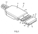
- To the total designated 10 connector include a plug 11 as a plug-in device and a device socket 12th
- the device socket 12 is for installation in an electronic device, e.g. a mobile phone, a small computer or the like. certainly. It comprises a plastic housing 13, in which a number of metallic contacts 14 is arranged.
- the contacts 14 are used with in Fig. 1 not visible end portions for contacting with contacts of the plug 11, also not shown there. Their visible in Figs. 1 to 3 other ends are as SMD-Lötfdirchen or possibly as Lötbeinchen for connection to a not shown printed circuit board formed. Shown is the contacting of the connector 10 in FIGS. 8 to 10.
- the plug 11 comprises a handle body 21 made of plastic and a kink protection sleeve 22 for a connected to the plug 11, not shown cable.
- the distance between two contacts 14 of the device socket 12 is designated 32.
- This contact spacing 32 which is also referred to as a grid, is naturally very small in the case of plug-in connections of highly miniaturized devices and is 1 mm or less.
- the plug 11 has an insulating body 33 and an embedded therein or anchored, the number of poles corresponding number of contacts 34 and 35.
- the contacts 34 and 35 are cut out of contact plate so-called.
- Each contact 34 and 35 has - each viewed in its longitudinal direction - a conductor connection portion 36 and 37, a clamping section 38 and 39 and a resilient contact legs 40 and 41, respectively.
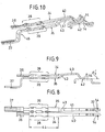
- the free end of this resilient contact leg 40 or 41 is, as illustrated in particular FIGS. 6, 7, 9 and 10, deformed to form a defined contact zone 42.
- the contacts 34 and 35 lie with their contact zones 42 when assembled connector 11 , 12 press-fit on the corresponding contacts 14 of the device socket 12 (see Fig. 9 and 10).
- Each two successive contacts 34 and 35 in a contact row are designed differently as described below.
- All contacts 34 and 35 are initially common that the contact zones 42 of their resilient contact legs 40, 41 are arranged in the same plane. This level is referred to in the non-contacted state of the connector 11, 12 in Figs. 6 and 7 with E 1 .
- the resilient contact legs 40 and 41 are biased against this plane E 1 , so that they easily when contacting the contact zones 42 on the contacts 14 of the device socket 12 bend upwards, as shown in Fig.9 in particular.
- all the contact zones 42 of all the contacts lie on a plane designated E 1 'in FIG. 9, which lies a little above the plane E 1 .
- the contacts 34 are, as shown in FIGS. 6 and 7 and 8 to 10, executed substantially straight in its longitudinal direction, one sees once from the bent, the contact zones 42 defining ends. In the main, the contacts 34 extend in a plane E 2 . In that regard, one can call the contacts 34 as 'undeformed' contacts.
- the contacts 35 are anchored with their Endspannabitesen 39 in each case in a deviating from the plane E 2 level (E 3 in Fig. 7) in Isollerstoff emotions 33 of the plug 11. Therefore, the contacts 35 each have an offset 43 and may be referred to as 'deformed' contacts.
- a contact 34 and a contact 35 alternately follow each other in the exemplary embodiment.
- contacts 34 and 35 can be housed and fixed with relatively wide Einspannabitesen 38 and 39 in the plug 11, which would otherwise not be possible because when arranged in the same plane and the same width of the clamping sections 38 and 39 in the insulating body 33 of the Plug 11 not enough plastic material for holding the contacts 34 and 35 would be available or provided.
- the width of the contacts in one of the Fig. 8 designated 44 length range can be very large, approximately equal to the contact distance 32.
- the area 44 includes the clamping portions 38 and 39 and an initial portion of resilient contact legs 40 and 41. As Figure 8 further shows, the resilient contact legs 40 and 41 are then narrowed towards their free ends.
- the contacts 35 have yet another substantially S- or Z-shaped crimp 45 between the gripping portion 39 and the lead terminal portion 37 which defines another plane E 4 ( Figure 7).
- the conductor connection portion 37 of the contact type 35 is otherwise longer than the conductor connection portion 36 of the contact 34. In this way - see.
- Figs. 4 and 8 - it is achieved that the stripped ends of the conductors to be connected can be soldered in a simple manner to the conductor connection sections 36 and 37, which are easily accessible in all respects.
- a connector 10 Shown and described is a connector 10, wherein the contacts 14 in the device socket 12 as well as the contact zones 42 of the contacts 34 and 35 of the associated connector 11 are each arranged in a single row. This should be the rule for connectors of the type in question here. In this case, the clamping portions 38 and 39 of the contacts 34 and 35 are seen to be arranged in the two planes E 2 and E 3 .
- each row of contacts care must be taken that within each row of contacts the contacts are arranged with their anchoring sections in different planes so that they can be accommodated with high pole density within the insulating body 33 of the plug 11 and securely held therein.
- the plug-in projection 20 of the plug 11 a plate 18, on whose narrow sides locking members 17 are formed, which cooperate with the metal bracket 15 of the device socket 12.
- the locking members 17 are formed as forms 24 of a metal strip 25.
- the metal strips 25 are freed by means of longitudinal cut-26 from the sheet 18.
- the special feature is that the two narrow ends 27 of the metal strip 25 remain connected to the plate 18.
- the locking members 17 thus have no projecting end, which can catch foreign objects and the locking members 24 could bend.
- a metal strip 25 with expression 24 has a greater length than they would have the only initially exempted by the free cuts 26 flat sheet metal strip. Due to the deformation 24, a longer length has formed, which leads to a certain material stretching, which in turn causes a strain hardening, which makes the locking member 24, especially on its surface, very strong and stable.
- the Gegenrastorgane 16 on the device socket 12 are each formed by a peripheral edge 28 of a punched in each side of the metal bracket 15 window 29, by cutting and Herausformen a window 29 issuellenden sheet metal strip 30.
- the metal strip 30 remains with its root 31 on the metal bracket 15th connected and is - as esp. From Fig. 11 can be seen clearly - outside the window 29 out.
- the metal strip 30 - esp. Together with the plug-side locking member 17 - closes the window 29 so that no contaminants from the interior of the device socket 12 can penetrate into the device.
Landscapes
- Engineering & Computer Science (AREA)
- Manufacturing & Machinery (AREA)
- Coupling Device And Connection With Printed Circuit (AREA)
- Details Of Connecting Devices For Male And Female Coupling (AREA)
- Connector Housings Or Holding Contact Members (AREA)
- Connections By Means Of Piercing Elements, Nuts, Or Screws (AREA)
Applications Claiming Priority (2)
| Application Number | Priority Date | Filing Date | Title |
|---|---|---|---|
| DE10358078A DE10358078B3 (de) | 2003-12-10 | 2003-12-10 | Elektrische Steckvorrichtung bzw. Steckverbindung |
| EP04024474A EP1542319B1 (fr) | 2003-12-10 | 2004-10-14 | Connecteur et connexion électrique |
Related Parent Applications (1)
| Application Number | Title | Priority Date | Filing Date |
|---|---|---|---|
| EP04024474A Division EP1542319B1 (fr) | 2003-12-10 | 2004-10-14 | Connecteur et connexion électrique |
Publications (3)
| Publication Number | Publication Date |
|---|---|
| EP1753090A2 true EP1753090A2 (fr) | 2007-02-14 |
| EP1753090A3 EP1753090A3 (fr) | 2007-07-18 |
| EP1753090B1 EP1753090B1 (fr) | 2008-07-09 |
Family
ID=34178056
Family Applications (2)
| Application Number | Title | Priority Date | Filing Date |
|---|---|---|---|
| EP04024474A Expired - Lifetime EP1542319B1 (fr) | 2003-12-10 | 2004-10-14 | Connecteur et connexion électrique |
| EP06022897A Expired - Lifetime EP1753090B1 (fr) | 2003-12-10 | 2004-10-14 | Connecteur et connexion électrique |
Family Applications Before (1)
| Application Number | Title | Priority Date | Filing Date |
|---|---|---|---|
| EP04024474A Expired - Lifetime EP1542319B1 (fr) | 2003-12-10 | 2004-10-14 | Connecteur et connexion électrique |
Country Status (8)
| Country | Link |
|---|---|
| US (1) | US7074076B2 (fr) |
| EP (2) | EP1542319B1 (fr) |
| JP (1) | JP2005174942A (fr) |
| CN (2) | CN101174744A (fr) |
| AT (1) | ATE353480T1 (fr) |
| BR (1) | BRPI0405394A (fr) |
| DE (3) | DE10358078B3 (fr) |
| DK (2) | DK1542319T3 (fr) |
Cited By (1)
| Publication number | Priority date | Publication date | Assignee | Title |
|---|---|---|---|---|
| CN106207613A (zh) * | 2016-07-15 | 2016-12-07 | 广州视源电子科技股份有限公司 | 一种数据线插头及其插拔连接结构 |
Families Citing this family (8)
| Publication number | Priority date | Publication date | Assignee | Title |
|---|---|---|---|---|
| US7371118B2 (en) * | 2006-08-25 | 2008-05-13 | Hon Hai Precision Ind. Co., Ltd | Electrical connector assembly with reduced crosstalk and electromaganetic interference |
| CN102341970B (zh) * | 2009-01-20 | 2014-04-30 | 莫列斯公司 | 具有外部emi屏蔽性能的插塞式连接器 |
| MY183625A (en) * | 2009-11-11 | 2021-03-03 | Mimos Berhad | Elastomeric interface connector |
| CN102655295A (zh) * | 2011-03-04 | 2012-09-05 | 艾恩特精密工业股份有限公司 | 薄型插头连接器及其组装方法 |
| CN102751607B (zh) * | 2012-07-04 | 2015-03-04 | 东莞市胜蓝电子有限公司 | 一种双排焊接式连接器 |
| JP2014086208A (ja) * | 2012-10-22 | 2014-05-12 | Hosiden Corp | コネクタ及びこれを備えた電子機器 |
| US9293858B2 (en) * | 2014-05-26 | 2016-03-22 | Bren-Tronics, Inc. | Screw down connector |
| KR102188058B1 (ko) * | 2015-06-25 | 2020-12-08 | 엘에스엠트론 주식회사 | 케이블 커넥터 |
Family Cites Families (10)
| Publication number | Priority date | Publication date | Assignee | Title |
|---|---|---|---|---|
| JP2522575B2 (ja) * | 1990-03-01 | 1996-08-07 | 矢崎総業株式会社 | 電気コネクタ |
| US5692928A (en) * | 1996-05-10 | 1997-12-02 | Molex Incorporated | Electrical connector having terminals with improved retention means |
| DE19621614C1 (de) * | 1996-05-30 | 1997-12-18 | Itt Cannon Gmbh | Steckverbinder |
| US5785556A (en) * | 1996-07-16 | 1998-07-28 | Molex Incorporated | Edge connector for a printed circuit board |
| US6139373A (en) * | 1997-04-08 | 2000-10-31 | Thomas & Betts International, Inc. | Multi-pin electrical connectors |
| JP3287810B2 (ja) * | 1999-04-28 | 2002-06-04 | モレックス インコーポレーテッド | 電気コネクタ |
| US6599136B2 (en) * | 2001-01-16 | 2003-07-29 | Hewlett-Packard Development Company, L.P. | Socket apparatus for a plug-in module |
| DE10104288C1 (de) * | 2001-01-30 | 2002-04-04 | Karl Lumberg Gmbh & Co Kg | Elektrische Steckverbindung |
| US6431918B1 (en) * | 2001-04-27 | 2002-08-13 | Hon Hai Precisionind. Co., Ltd. | Modular jack connector meeting 1000base-T specifications |
| TW491419U (en) * | 2001-07-20 | 2002-06-11 | Hon Hai Prec Ind Co Ltd | Electrical connector |
-
2003
- 2003-12-10 DE DE10358078A patent/DE10358078B3/de not_active Expired - Fee Related
-
2004
- 2004-10-14 DK DK04024474T patent/DK1542319T3/da active
- 2004-10-14 AT AT04024474T patent/ATE353480T1/de not_active IP Right Cessation
- 2004-10-14 DK DK06022897T patent/DK1753090T3/da active
- 2004-10-14 DE DE502004002850T patent/DE502004002850D1/de not_active Expired - Fee Related
- 2004-10-14 EP EP04024474A patent/EP1542319B1/fr not_active Expired - Lifetime
- 2004-10-14 DE DE502004007583T patent/DE502004007583D1/de not_active Expired - Lifetime
- 2004-10-14 EP EP06022897A patent/EP1753090B1/fr not_active Expired - Lifetime
- 2004-11-26 JP JP2004372271A patent/JP2005174942A/ja active Pending
- 2004-12-01 US US11/001,697 patent/US7074076B2/en not_active Expired - Fee Related
- 2004-12-06 BR BR0405394-0A patent/BRPI0405394A/pt not_active IP Right Cessation
- 2004-12-10 CN CNA2007101812374A patent/CN101174744A/zh active Pending
- 2004-12-10 CN CNB2004101002797A patent/CN100466383C/zh not_active Expired - Fee Related
Cited By (1)
| Publication number | Priority date | Publication date | Assignee | Title |
|---|---|---|---|---|
| CN106207613A (zh) * | 2016-07-15 | 2016-12-07 | 广州视源电子科技股份有限公司 | 一种数据线插头及其插拔连接结构 |
Also Published As
| Publication number | Publication date |
|---|---|
| JP2005174942A (ja) | 2005-06-30 |
| CN100466383C (zh) | 2009-03-04 |
| EP1753090B1 (fr) | 2008-07-09 |
| HK1078687A1 (zh) | 2006-03-17 |
| EP1542319A3 (fr) | 2005-07-06 |
| CN1638197A (zh) | 2005-07-13 |
| DK1753090T3 (da) | 2008-08-11 |
| EP1753090A3 (fr) | 2007-07-18 |
| EP1542319A2 (fr) | 2005-06-15 |
| DE502004002850D1 (de) | 2007-03-22 |
| US20050130461A1 (en) | 2005-06-16 |
| CN101174744A (zh) | 2008-05-07 |
| DE502004007583D1 (de) | 2008-08-21 |
| EP1542319B1 (fr) | 2007-02-07 |
| BRPI0405394A (pt) | 2005-08-30 |
| DK1542319T3 (da) | 2007-03-12 |
| US7074076B2 (en) | 2006-07-11 |
| DE10358078B3 (de) | 2005-03-10 |
| ATE353480T1 (de) | 2007-02-15 |
Similar Documents
| Publication | Publication Date | Title |
|---|---|---|
| DE102013110082C5 (de) | Steckverbinder | |
| EP3159974B2 (fr) | Borne d'alimentation électrique | |
| DE102010014144B4 (de) | Elektrische Anschlussklemme | |
| DE69300865T3 (de) | Elektrischer verbinder mit blech als steckkontaktmaterial. | |
| DE102008009357A1 (de) | Elektrische Anschlusseinrichtung | |
| EP2107648B1 (fr) | Connecteur avec une plaque de support utilisée comme blindage | |
| EP3375048B1 (fr) | Contact à enficher | |
| EP2026417B1 (fr) | Connecteur électrique doté d'éléments de contact hermaphrodites | |
| EP1542319B1 (fr) | Connecteur et connexion électrique | |
| DE102007026102B3 (de) | Steckverbinder für Leiterplatten | |
| DE60223319T2 (de) | Elektrischer Verbinder zum Aufnahme eines Steckers | |
| DE202010018429U1 (de) | Betätigungseinrichtung für eine elektrische Anschlussklemme | |
| EP0921597B1 (fr) | Ressort de contact | |
| DE20319254U1 (de) | Elektrische Steckvorrichtung bzw. Steckverbindung | |
| DE29907005U1 (de) | Anschluß- und/oder Verbindungsklemme für ein elektrisches Gerät | |
| DE202023103986U1 (de) | Leiteranschlussklemme | |
| DE102023109918A1 (de) | Reihenklemme mit Ausbruchfenster | |
| WO2025214545A1 (fr) | Outil d'assemblage pour connecteur enfichable et son procédé d'utilisation | |
| DE1765412A1 (de) | Elektrische Verbinderbuchse zum Aufnehmen und Festhalten eines elektrischen Gegenkontaktes | |
| DE9405949U1 (de) | Elektrischer Kontakt zum Anschluß von mindestens zwei Leitern | |
| DE2424489A1 (de) | Elektrische steckverbindung | |
| DE1928775A1 (de) | Loesbare elektrische Steckverbindung |
Legal Events
| Date | Code | Title | Description |
|---|---|---|---|
| PUAI | Public reference made under article 153(3) epc to a published international application that has entered the european phase |
Free format text: ORIGINAL CODE: 0009012 |
|
| AC | Divisional application: reference to earlier application |
Ref document number: 1542319 Country of ref document: EP Kind code of ref document: P |
|
| AK | Designated contracting states |
Kind code of ref document: A2 Designated state(s): AT BE BG CH CY CZ DE DK EE ES FI FR GB GR HU IE IT LI LU MC NL PL PT RO SE SI SK TR |
|
| RAP1 | Party data changed (applicant data changed or rights of an application transferred) |
Owner name: LUMBERG CONNECT GMBH |
|
| PUAL | Search report despatched |
Free format text: ORIGINAL CODE: 0009013 |
|
| AK | Designated contracting states |
Kind code of ref document: A3 Designated state(s): AT BE BG CH CY CZ DE DK EE ES FI FR GB GR HU IE IT LI LU MC NL PL PT RO SE SI SK TR |
|
| 17P | Request for examination filed |
Effective date: 20070704 |
|
| GRAP | Despatch of communication of intention to grant a patent |
Free format text: ORIGINAL CODE: EPIDOSNIGR1 |
|
| GRAS | Grant fee paid |
Free format text: ORIGINAL CODE: EPIDOSNIGR3 |
|
| AKX | Designation fees paid |
Designated state(s): CZ DE DK FI IT SE |
|
| GRAA | (expected) grant |
Free format text: ORIGINAL CODE: 0009210 |
|
| AC | Divisional application: reference to earlier application |
Ref document number: 1542319 Country of ref document: EP Kind code of ref document: P |
|
| AK | Designated contracting states |
Kind code of ref document: B1 Designated state(s): CZ DE DK FI IT SE |
|
| REG | Reference to a national code |
Ref country code: DK Ref legal event code: T3 |
|
| REF | Corresponds to: |
Ref document number: 502004007583 Country of ref document: DE Date of ref document: 20080821 Kind code of ref document: P |
|
| REG | Reference to a national code |
Ref country code: SE Ref legal event code: TRGR |
|
| PGFP | Annual fee paid to national office [announced via postgrant information from national office to epo] |
Ref country code: DK Payment date: 20081010 Year of fee payment: 5 |
|
| PGFP | Annual fee paid to national office [announced via postgrant information from national office to epo] |
Ref country code: IT Payment date: 20080929 Year of fee payment: 5 |
|
| PLBE | No opposition filed within time limit |
Free format text: ORIGINAL CODE: 0009261 |
|
| STAA | Information on the status of an ep patent application or granted ep patent |
Free format text: STATUS: NO OPPOSITION FILED WITHIN TIME LIMIT |
|
| 26N | No opposition filed |
Effective date: 20090414 |
|
| PG25 | Lapsed in a contracting state [announced via postgrant information from national office to epo] |
Ref country code: CZ Free format text: LAPSE BECAUSE OF NON-PAYMENT OF DUE FEES Effective date: 20081014 |
|
| PGFP | Annual fee paid to national office [announced via postgrant information from national office to epo] |
Ref country code: SE Payment date: 20091026 Year of fee payment: 6 |
|
| REG | Reference to a national code |
Ref country code: DK Ref legal event code: EBP |
|
| PG25 | Lapsed in a contracting state [announced via postgrant information from national office to epo] |
Ref country code: DK Free format text: LAPSE BECAUSE OF NON-PAYMENT OF DUE FEES Effective date: 20091031 |
|
| PG25 | Lapsed in a contracting state [announced via postgrant information from national office to epo] |
Ref country code: IT Free format text: LAPSE BECAUSE OF NON-PAYMENT OF DUE FEES Effective date: 20091014 |
|
| PG25 | Lapsed in a contracting state [announced via postgrant information from national office to epo] |
Ref country code: SE Free format text: LAPSE BECAUSE OF NON-PAYMENT OF DUE FEES Effective date: 20101015 |
|
| PGFP | Annual fee paid to national office [announced via postgrant information from national office to epo] |
Ref country code: FI Payment date: 20111007 Year of fee payment: 8 |
|
| REG | Reference to a national code |
Ref country code: DE Ref legal event code: R082 Ref document number: 502004007583 Country of ref document: DE Representative=s name: PATENTANWAELTE OSTRIGA, SONNET, WIRTHS & VORWE, DE |
|
| PG25 | Lapsed in a contracting state [announced via postgrant information from national office to epo] |
Ref country code: FI Free format text: LAPSE BECAUSE OF NON-PAYMENT OF DUE FEES Effective date: 20121014 |
|
| PGFP | Annual fee paid to national office [announced via postgrant information from national office to epo] |
Ref country code: DE Payment date: 20160825 Year of fee payment: 13 |
|
| REG | Reference to a national code |
Ref country code: DE Ref legal event code: R119 Ref document number: 502004007583 Country of ref document: DE |
|
| PG25 | Lapsed in a contracting state [announced via postgrant information from national office to epo] |
Ref country code: DE Free format text: LAPSE BECAUSE OF NON-PAYMENT OF DUE FEES Effective date: 20180501 |