EP1754308B1 - Circuit et procede d'amelioration du facteur q - Google Patents
Circuit et procede d'amelioration du facteur q Download PDFInfo
- Publication number
- EP1754308B1 EP1754308B1 EP05735127A EP05735127A EP1754308B1 EP 1754308 B1 EP1754308 B1 EP 1754308B1 EP 05735127 A EP05735127 A EP 05735127A EP 05735127 A EP05735127 A EP 05735127A EP 1754308 B1 EP1754308 B1 EP 1754308B1
- Authority
- EP
- European Patent Office
- Prior art keywords
- transistor
- resistance
- enhancement circuit
- terminal
- component
- Prior art date
- Legal status (The legal status is an assumption and is not a legal conclusion. Google has not performed a legal analysis and makes no representation as to the accuracy of the status listed.)
- Expired - Fee Related
Links
- 238000000034 method Methods 0.000 title description 8
- 230000003071 parasitic effect Effects 0.000 claims description 15
- 238000010586 diagram Methods 0.000 description 12
- 239000003990 capacitor Substances 0.000 description 7
- 238000012545 processing Methods 0.000 description 4
- 238000013459 approach Methods 0.000 description 3
- 238000004891 communication Methods 0.000 description 3
- 230000000694 effects Effects 0.000 description 3
- 230000002708 enhancing effect Effects 0.000 description 3
- 238000012986 modification Methods 0.000 description 2
- 230000004048 modification Effects 0.000 description 2
- 238000006243 chemical reaction Methods 0.000 description 1
- 238000013016 damping Methods 0.000 description 1
- 230000005669 field effect Effects 0.000 description 1
- 230000001939 inductive effect Effects 0.000 description 1
- 229910044991 metal oxide Inorganic materials 0.000 description 1
- 150000004706 metal oxides Chemical class 0.000 description 1
- 239000004065 semiconductor Substances 0.000 description 1
Images

Classifications
-
- H—ELECTRICITY
- H03—ELECTRONIC CIRCUITRY
- H03H—IMPEDANCE NETWORKS, e.g. RESONANT CIRCUITS; RESONATORS
- H03H11/00—Networks using active elements
- H03H11/02—Multiple-port networks
- H03H11/04—Frequency selective two-port networks
- H03H11/10—Frequency selective two-port networks using negative impedance converters
-
- H—ELECTRICITY
- H03—ELECTRONIC CIRCUITRY
- H03H—IMPEDANCE NETWORKS, e.g. RESONANT CIRCUITS; RESONATORS
- H03H11/00—Networks using active elements
- H03H11/46—One-port networks
- H03H11/52—One-port networks simulating negative resistances
-
- H—ELECTRICITY
- H03—ELECTRONIC CIRCUITRY
- H03H—IMPEDANCE NETWORKS, e.g. RESONANT CIRCUITS; RESONATORS
- H03H7/00—Multiple-port networks comprising only passive electrical elements as network components
- H03H7/01—Frequency selective two-port networks
- H03H7/03—Frequency selective two-port networks comprising means for compensation of loss
Definitions
- the present invention relates to electrical and electronic circuits and systems. More specifically, the present invention relates to systems and methods for Q enhancement for passive inductive capacitive resonators in electrical and electronic circuits and systems.
- Q is a "quality factor.”
- Q is a measure of the sharpness of the resonant peak in the frequency response of the system and is inversely proportional to the damping in the system:
- Q center frequency divided by Hz bandwidth.
- Equalizers that contain resonant circuits are rated by their Q-value: the higher the Q, the higher and more well defined the peak in the response.
- the ratio of a bandpass or band-reject filter's center frequency to its bandwidth defines Q.
- Q is inversely proportional to bandwidth, i.e., a higher Q indicates a narrower bandwidth.
- Q enhancement circuits typically use negative resistor circuits to cancel out parasitic serial resistance associated with the inductors (L) in the passive inductor-capacitor (LC) resonators.
- L inductors
- LC passive inductor-capacitor
- US-A-5343142 When implemented in fully differential mode, these circuits are usually connected in parallel with the capacitors of the resonator and typically the capacitor is connected between two inductors.
- the negative resistor circuits fail to adequately cancel the parasitic resistance of the inductors. This non-ideal cancellation causes other second order effects and can cause the circuit to resonate at other frequencies.
- negative resistors require voltage-to-current converters to generate negative currents for the cancellation. This makes the negative resistor circuit more susceptible to non-linear distortion and circuit delay and degrades the performance of the LC resonator.
- a need remains in the art for a system or method for enhancing the Q of a circuit.
- a need remains in the art for a system or method for enhancing the Q of LC resonators used in analog signal processing and communication systems to improve the linearity and resolution thereof.
- the need in the art is addressed by the Q enhancement circuit and method of the present invention.
- the inventive circuit is adapted for use with a component having a parasitic resistance R L1 and a first resistance R 1 disposed in series with the component and an arrangement for making the resistance a negative resistance.
- First and second inductors constitute the components for which Q enhancement is effected.
- a resistance R 1 is disposed in series with the first inductor and is equal to the parasitic resistance R L1 thereof.
- a second resistance R 2 is disposed in series with the second inductor and is equal to the parasitic resistance R L2 thereof.
- the Q enhancement circuit includes a first transistor Q 1 and a second transistor Q 2 .
- the transistors may be BJT (bipolar junction transistor), MOSFETs (metal-oxide semiconductor field effect transistors), or other type of transistors.
- each of the collector terminals is connected to a respective one of the first or the second resistors R 1 or R 2 and each of the emitters are connected to a respective one of the inductors.
- the Q enhancement circuit includes a first unity-gain amplifier (emitter follower/voltage follower) connected between the collector terminal of the first transistor and the base terminal of the second transistor and a second unity-gain amplifier connected between the collector terminal of the second transistor and the base terminal of the first transistor.
- each of the transistors has a source, a gate and a drain terminal.
- each of the drain terminals is connected to a respective one of the first or the second resistors R 1 or R 2 and the source terminals are connected to a respective one of the inductors.
- a first unity-gain amplifier (source follower) is connected between the drain terminal of the first transistor and the gate terminal of the second transistor and a second unity-gain amplifier connected between the drain terminal of the second transistor and the gate terminal of the first transistor.
- each of the unity gain amplifier is a emitter/source follower to achieve optimal circuit simplicity and maximal operating bandwidth.
- Figure 1 is a schematic diagram showing a differential LC resonator widely used for analog signal processing in accordance with conventional teachings.
- Figure 2 is a schematic diagram of the resonator of Figure 1 showing parasitic resistance of the inductors thereof.
- the resonator 10' includes first and second inductors L 1 and L 2 connected in parallel to a ground connection on one end and a capacitor C connected across the other ends thereof.
- the first and second inductors L 1 and L 2 have inherent parasitic resistance shown as, respectively, as illustrated in Figure 2 .
- FIG 3 shows an approach for Q enhancement of the resonator of Figure 2 in accordance with conventional teachings.
- a negative resistor R is connected in parallel with the capacitor C.
- this approach can increase the Q of the resonator, it has not been found adequate in the cancellation of the effect of the parasitic serial resistors R L1 and R L2 on Q.
- the negative resistor R makes the resonator a more complicated circuit and can cause resonance at other undesired frequencies.
- a need remains in the art for a system or method for enhancing the Q of a circuit.
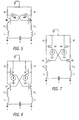
- FIG 4 is a schematic diagram of a resonator with Q enhancement implemented in accordance with an illustrative embodiment of the teachings of the present invention.
- the resonator 40 is similar to that of Figure 2 with the exception that first and second negative resistors - R 1 and - R 2 are disposed in series with the first and second inductors L 1 and L 2 , respectively.
- FIG. 5 is a schematic diagram of the resonator of Figure 4 with an illustrative implementation of the negative resistors thereof.
- resistors R 1 and R 2 are disposed in series with the first and second inductors.
- the resistors R 1 and R 2 should be equal to the parasitic serial resistors R L1 and R L2 .
- First and second transistors Q 1 and Q 2 are connected in between the resistors R 1 and R 2 and the associated component, in the illustrative application, the first and second inductors L 1 and L 2 , respectively.
- the collector of Q 1 is connected to R 1 at a node A and the collector of Q 2 is connected to R 2 at a node B.
- a first voltage follower (unity-gain amplifier) 42 is connected between node A and the base of Q2.
- the second voltage follower 44 is connected between node B and the base of Q1.
- the first and second voltage followers 42 and 44 can be implemented by emitter followers as shown in Figure 6 below, source followers as shown in Figure 7 or other suitable circuit arrangement as will be appreciated by those of ordinary skill in the art.
- Figure 6 is a schematic diagram of the resonator of Figure 5 with a bipolar emitter follower implementation for the voltage followers thereof.
- the first follower 42 is implemented with a third bipolar transistor Q 3 having its base connected to node A, its collector connected to ground and its emitter connected to a first current source 46.
- the second follower 44 is implemented with a fourth bipolar transistor Q 4 having its base connected to node B, its collector connected to ground and its emitter connected to a second current source 48. While an NPN implementation is shown, those skilled in the art will appreciate that a PNP implementation may be employed as well.
- FIG. 7 is a schematic diagram of the resonator of Figure 5 with a MOSFET source follower implementation for the voltage followers thereof.
- n-channel MOSFETs M 1 and M 2 are used in place of the first and second transistors Q 1 and Q 2 of Figure 6 .
- the first follower 42 is implemented with a third MOSFET transistor M 3 having its gate connected to node A, its drain connected to ground and its source connected to the first current source 46.
- the second follower 44 is implemented with a fourth MOSFET transistor M 4 having its gate connected to node B, its drain connected to ground and its source connected to the second current source 48. While an n-channel implementation is shown, those skilled in the art will appreciate that a p-channel implementation may be employed as well.
- the inventive enhancement circuit 40 should cancel the effect of the inherent parasitic resistance and improve the Q factor of the components with which it is used.
Landscapes
- Amplifiers (AREA)
- Inductance-Capacitance Distribution Constants And Capacitance-Resistance Oscillators (AREA)
- Networks Using Active Elements (AREA)
- Filters And Equalizers (AREA)
- Paper (AREA)
Claims (10)
- Circuit (40) d'amélioration du facteur Q pour un premier composant (L1) ayant une première résistance parasite (RL1), ledit circuit d'amélioration comportant :une première résistance (R1) disposée en séries avec ledit premier composant ;un premier moyen destiné à faire de ladite première résistance disposée en séries avec ledit composant une résistance négative ;un second composant (L2) ayant une seconde résistance parasite (RL2) ; etune seconde résistance (R2) disposée en séries avec ledit second composant (L2) et ledit second moyen pour faire de ladite seconde résistance (R2) une résistance négative,dans lequel ladite première résistance (R1) disposée en séries avec ledit premier composant est égale à ladite première résistance parasite (RL1) ; ledit premier moyen pour faire de ladite première résistance (R1) une résistance négative comprend un premier transistor Q1 ; ledit second moyen pour faire de ladite seconde résistance une résistance négative comprend un second transistor Q2 ; chacun desdits transistors a une borne de collecteur, une borne de base et une borne d'émetteur ; et chacune desdites bornes de collecteur est connectée à l'une, respective, desdites première et seconde résistances (R1, R2), et lesdits émetteurs sont connectés à l'un, respectif, desdits premier et second composants (L1, L2) .
- Circuit d'amélioration du facteur Q selon la revendication 1, dans lequel ledit premier composant est une inductance (L1) .
- Circuit d'amélioration du facteur Q selon la revendication 1, lequel circuit d'amélioration du facteur Q comprend un premier amplificateur (42) connecté entre la borne de collecteur du premier transistor et la borne de base du second transistor et un second amplificateur (44) connecté entre la borne de collecteur dudit second transistor et ladite borne de base dudit premier transistor.
- Circuit d'amélioration du facteur Q selon la revendication 3, dans lequel chacun desdits amplificateurs est un amplificateur à gain unité.
- Circuit d'amélioration du facteur Q selon la revendication 4, dans lequel chacun desdits amplificateurs est un montage à émetteur suiveur.
- Circuit d'amélioration du facteur Q selon la revendication 1, dans lequel chacun desdits transistors comporte une borne de source, une borne de grille et une borne de drain au lieu d'une borne de collecteur, d'une borne de base et d'une borne d'émetteur, respectivement.
- Circuit d'amélioration du facteur Q selon la revendication 6, dans lequel chacune desdites bornes de drain est connectée à l'une, respective, desdites première et seconde résistances (R1, R2) et lesdites bornes de source sont connectées à l'un, respectif, desdits premier et second composants (L1, L2) .
- Circuit d'amélioration du facteur Q selon la revendication 7, lequel circuit d'amélioration du facteur Q comprend un premier amplificateur (42) connecté entre la borne de drain du premier transistor et la borne de grille du second transistor, et un second amplificateur (44) connecté entre la borne de drain dudit second transistor et ladite borne de grille dudit premier transistor.
- Circuit d'amélioration du facteur Q selon la revendication 8, dans lequel chacun desdits amplificateurs est un amplificateur à gain unité.
- Circuit d'amélioration du facteur Q selon la revendication 9, dans lequel chacun desdits amplificateurs est un montage à source suiveuse.
Applications Claiming Priority (2)
| Application Number | Priority Date | Filing Date | Title |
|---|---|---|---|
| US10/864,158 US7202762B2 (en) | 2004-06-09 | 2004-06-09 | Q enhancement circuit and method |
| PCT/US2005/012300 WO2006001878A1 (fr) | 2004-06-09 | 2005-04-11 | Circuit et procede d'amelioration du facteur q |
Publications (2)
| Publication Number | Publication Date |
|---|---|
| EP1754308A1 EP1754308A1 (fr) | 2007-02-21 |
| EP1754308B1 true EP1754308B1 (fr) | 2008-09-03 |
Family
ID=34965205
Family Applications (1)
| Application Number | Title | Priority Date | Filing Date |
|---|---|---|---|
| EP05735127A Expired - Fee Related EP1754308B1 (fr) | 2004-06-09 | 2005-04-11 | Circuit et procede d'amelioration du facteur q |
Country Status (7)
| Country | Link |
|---|---|
| US (1) | US7202762B2 (fr) |
| EP (1) | EP1754308B1 (fr) |
| JP (1) | JP4659832B2 (fr) |
| KR (1) | KR100866235B1 (fr) |
| DE (1) | DE602005009526D1 (fr) |
| NO (1) | NO20070078L (fr) |
| WO (1) | WO2006001878A1 (fr) |
Families Citing this family (5)
| Publication number | Priority date | Publication date | Assignee | Title |
|---|---|---|---|---|
| US7884680B2 (en) * | 2008-06-30 | 2011-02-08 | Infineon Technologies Ag | Dynamically adjustable Q-factors |
| DE102009012767B4 (de) * | 2009-03-12 | 2013-05-23 | Texas Instruments Deutschland Gmbh | Geschaltete Spannungsversorgung mit Stromabtastung |
| US9124279B2 (en) * | 2012-09-03 | 2015-09-01 | Tensorcom, Inc. | Method and apparatus for an active negative-capacitor circuit to cancel the input capacitance of comparators |
| RU2712784C1 (ru) * | 2019-02-04 | 2020-01-31 | Федеральное государственное бюджетное образовательное учреждение высшего образования "Ростовский государственный университет путей сообщения" (ФГБОУ ВО РГУПС) | Способ измерения добротности резонатора |
| US11047139B2 (en) | 2019-07-09 | 2021-06-29 | Schluter Systems L.P. | Veneer profile with fastening feature and related methods |
Family Cites Families (14)
| Publication number | Priority date | Publication date | Assignee | Title |
|---|---|---|---|---|
| JP3381283B2 (ja) | 1991-12-24 | 2003-02-24 | 株式会社デンソー | 可変リアクタンス回路およびこれを用いた可変整合回路 |
| US5892425A (en) * | 1997-04-10 | 1999-04-06 | Virginia Tech Intellectual Properties, Inc. | Interwound center-tapped spiral inductor |
| JPH11330851A (ja) * | 1998-05-11 | 1999-11-30 | Matsushita Electric Ind Co Ltd | 発振器 |
| US6469586B1 (en) * | 2000-08-25 | 2002-10-22 | Sige Semiconductor Inc. | Low voltage voltage-controlled oscillator topology |
| US6681103B1 (en) * | 2000-08-25 | 2004-01-20 | Sige Semiconductor Inc. | On-chip image reject filter |
| US6778023B2 (en) | 2001-07-31 | 2004-08-17 | Nokia Corporation | Tunable filter and method of tuning a filter |
| JP2003045722A (ja) * | 2001-08-01 | 2003-02-14 | Sony Corp | インダクタ素子、および、インダクタ素子を用いた集積回路 |
| US6680655B2 (en) * | 2001-08-01 | 2004-01-20 | Sige Semiconductor Inc. | Automatic gain control for a voltage controlled oscillator |
| US6621331B2 (en) * | 2001-08-07 | 2003-09-16 | Hrl Laboratories, Llc | Variable negative resistance cell for bipolar integrated circuits |
| US6930562B2 (en) * | 2002-07-16 | 2005-08-16 | Matsushita Electric Industrial Co., Ltd. | Oscillation with multiple series circuits in parallel |
| US6650163B1 (en) * | 2002-08-08 | 2003-11-18 | International Business Machines Corporation | Clock generator for integrated circuit |
| US6970048B1 (en) * | 2003-12-12 | 2005-11-29 | National Semiconductor Corporation | Inductive-capacitive (LC) based quadrature voltage controlled oscillator (VCO) with deterministic quadrature signal phase relationship |
| US20050156681A1 (en) * | 2004-01-20 | 2005-07-21 | Koji Takinami | Voltage controlled oscillator |
| KR100615552B1 (ko) * | 2004-06-01 | 2006-08-25 | 학교법인 한국정보통신학원 | 직렬 교차 연결된 상보형 트랜지스터를 이용한 전압 제어발진기 및 이를 이용한 신호 송수신 장치 |
-
2004
- 2004-06-09 US US10/864,158 patent/US7202762B2/en not_active Expired - Fee Related
-
2005
- 2005-04-11 KR KR1020067025933A patent/KR100866235B1/ko not_active Expired - Fee Related
- 2005-04-11 EP EP05735127A patent/EP1754308B1/fr not_active Expired - Fee Related
- 2005-04-11 DE DE602005009526T patent/DE602005009526D1/de not_active Expired - Lifetime
- 2005-04-11 JP JP2007527230A patent/JP4659832B2/ja not_active Expired - Fee Related
- 2005-04-11 WO PCT/US2005/012300 patent/WO2006001878A1/fr not_active Ceased
-
2007
- 2007-01-05 NO NO20070078A patent/NO20070078L/no not_active Application Discontinuation
Also Published As
| Publication number | Publication date |
|---|---|
| NO20070078L (no) | 2007-01-05 |
| WO2006001878A1 (fr) | 2006-01-05 |
| JP2008503178A (ja) | 2008-01-31 |
| KR20070014196A (ko) | 2007-01-31 |
| EP1754308A1 (fr) | 2007-02-21 |
| KR100866235B1 (ko) | 2008-10-30 |
| JP4659832B2 (ja) | 2011-03-30 |
| US20050275490A1 (en) | 2005-12-15 |
| US7202762B2 (en) | 2007-04-10 |
| DE602005009526D1 (de) | 2008-10-16 |
Similar Documents
| Publication | Publication Date | Title |
|---|---|---|
| US7535323B2 (en) | Bulk acoustic wave filter with reduced nonlinear signal distortion | |
| EP1816742B1 (fr) | Amplificateur différentiel et système radio doté d'un amplificateur différentiel | |
| US6922108B2 (en) | Active balun circuit for single-ended to differential RF signal conversion with enhanced common-mode rejection | |
| CN101145760A (zh) | 具有较小失真度的低噪声混频器及方法 | |
| EP1754308B1 (fr) | Circuit et procede d'amelioration du facteur q | |
| FI100751B (fi) | Pienikohinainen vahvistin | |
| EP1142107B1 (fr) | Convertisseur actif differentiel-asymetrique | |
| JP3853604B2 (ja) | 周波数変換回路 | |
| US5099155A (en) | Active element filter network | |
| US20060290441A1 (en) | Quasi-Balun | |
| CN114640310B (zh) | 一种振荡电路和一种压控振荡器 | |
| WO2000055964A1 (fr) | Cellule de transconductance linearisee | |
| JP3332657B2 (ja) | ミキサ回路 | |
| JP2639808B2 (ja) | アクテイブフイルタ | |
| WO2013088337A1 (fr) | Circuit électronique à faible bruit simulant le comportement d'un inducteur | |
| JP4761851B2 (ja) | 帰還形信号処理回路 | |
| JP3300301B2 (ja) | 低域通過フィルタ | |
| EP1265357A1 (fr) | Circuit de commutation | |
| JP2007006302A (ja) | インピーダンス変換回路と、これを用いたハイパスフィルタ回路および周波数変換回路 | |
| JPH09148880A (ja) | 電子回路、これを用いたフィルタ装置及び無線装置 | |
| JP2007274179A (ja) | 同調回路及びこれに用いる可変利得減衰器 | |
| JPH06350375A (ja) | 整合回路 | |
| CN116827272A (zh) | 一种斩波放大器电路及设备 | |
| CN119543853A (zh) | 一种功率放大电路、电子电路及电子设备 | |
| CN115632672A (zh) | 具有反馈校正机制的通信设备 |
Legal Events
| Date | Code | Title | Description |
|---|---|---|---|
| PUAI | Public reference made under article 153(3) epc to a published international application that has entered the european phase |
Free format text: ORIGINAL CODE: 0009012 |
|
| 17P | Request for examination filed |
Effective date: 20061114 |
|
| AK | Designated contracting states |
Kind code of ref document: A1 Designated state(s): DE FR SE |
|
| DAX | Request for extension of the european patent (deleted) | ||
| RBV | Designated contracting states (corrected) |
Designated state(s): DE FR SE |
|
| GRAP | Despatch of communication of intention to grant a patent |
Free format text: ORIGINAL CODE: EPIDOSNIGR1 |
|
| GRAS | Grant fee paid |
Free format text: ORIGINAL CODE: EPIDOSNIGR3 |
|
| GRAA | (expected) grant |
Free format text: ORIGINAL CODE: 0009210 |
|
| AK | Designated contracting states |
Kind code of ref document: B1 Designated state(s): DE FR SE |
|
| REF | Corresponds to: |
Ref document number: 602005009526 Country of ref document: DE Date of ref document: 20081016 Kind code of ref document: P |
|
| REG | Reference to a national code |
Ref country code: SE Ref legal event code: TRGR |
|
| PLBE | No opposition filed within time limit |
Free format text: ORIGINAL CODE: 0009261 |
|
| STAA | Information on the status of an ep patent application or granted ep patent |
Free format text: STATUS: NO OPPOSITION FILED WITHIN TIME LIMIT |
|
| 26N | No opposition filed |
Effective date: 20090604 |
|
| PGFP | Annual fee paid to national office [announced via postgrant information from national office to epo] |
Ref country code: DE Payment date: 20110406 Year of fee payment: 7 Ref country code: FR Payment date: 20110426 Year of fee payment: 7 Ref country code: SE Payment date: 20110412 Year of fee payment: 7 |
|
| REG | Reference to a national code |
Ref country code: SE Ref legal event code: EUG |
|
| REG | Reference to a national code |
Ref country code: FR Ref legal event code: ST Effective date: 20121228 |
|
| REG | Reference to a national code |
Ref country code: DE Ref legal event code: R119 Ref document number: 602005009526 Country of ref document: DE Effective date: 20121101 |
|
| PG25 | Lapsed in a contracting state [announced via postgrant information from national office to epo] |
Ref country code: FR Free format text: LAPSE BECAUSE OF NON-PAYMENT OF DUE FEES Effective date: 20120430 Ref country code: SE Free format text: LAPSE BECAUSE OF NON-PAYMENT OF DUE FEES Effective date: 20120412 |
|
| PG25 | Lapsed in a contracting state [announced via postgrant information from national office to epo] |
Ref country code: DE Free format text: LAPSE BECAUSE OF NON-PAYMENT OF DUE FEES Effective date: 20121101 |