EP1755103B1 - Dispositif d'affichage électroluminescent organique ayant un dispositif de contrôle d'émission générant des signaux de contrôle d'émission - Google Patents
Dispositif d'affichage électroluminescent organique ayant un dispositif de contrôle d'émission générant des signaux de contrôle d'émission Download PDFInfo
- Publication number
- EP1755103B1 EP1755103B1 EP06254019A EP06254019A EP1755103B1 EP 1755103 B1 EP1755103 B1 EP 1755103B1 EP 06254019 A EP06254019 A EP 06254019A EP 06254019 A EP06254019 A EP 06254019A EP 1755103 B1 EP1755103 B1 EP 1755103B1
- Authority
- EP
- European Patent Office
- Prior art keywords
- transistor
- output signal
- signal
- emission control
- flip
- Prior art date
- Legal status (The legal status is an assumption and is not a legal conclusion. Google has not performed a legal analysis and makes no representation as to the accuracy of the status listed.)
- Not-in-force
Links
Images




Classifications
-
- G—PHYSICS
- G09—EDUCATION; CRYPTOGRAPHY; DISPLAY; ADVERTISING; SEALS
- G09G—ARRANGEMENTS OR CIRCUITS FOR CONTROL OF INDICATING DEVICES USING STATIC MEANS TO PRESENT VARIABLE INFORMATION
- G09G3/00—Control arrangements or circuits, of interest only in connection with visual indicators other than cathode-ray tubes
- G09G3/20—Control arrangements or circuits, of interest only in connection with visual indicators other than cathode-ray tubes for presentation of an assembly of a number of characters, e.g. a page, by composing the assembly by combination of individual elements arranged in a matrix no fixed position being assigned to or needed to be assigned to the individual characters or partial characters
- G09G3/22—Control arrangements or circuits, of interest only in connection with visual indicators other than cathode-ray tubes for presentation of an assembly of a number of characters, e.g. a page, by composing the assembly by combination of individual elements arranged in a matrix no fixed position being assigned to or needed to be assigned to the individual characters or partial characters using controlled light sources
- G09G3/30—Control arrangements or circuits, of interest only in connection with visual indicators other than cathode-ray tubes for presentation of an assembly of a number of characters, e.g. a page, by composing the assembly by combination of individual elements arranged in a matrix no fixed position being assigned to or needed to be assigned to the individual characters or partial characters using controlled light sources using electroluminescent panels
- G09G3/32—Control arrangements or circuits, of interest only in connection with visual indicators other than cathode-ray tubes for presentation of an assembly of a number of characters, e.g. a page, by composing the assembly by combination of individual elements arranged in a matrix no fixed position being assigned to or needed to be assigned to the individual characters or partial characters using controlled light sources using electroluminescent panels semiconductive, e.g. using light-emitting diodes [LED]
- G09G3/3208—Control arrangements or circuits, of interest only in connection with visual indicators other than cathode-ray tubes for presentation of an assembly of a number of characters, e.g. a page, by composing the assembly by combination of individual elements arranged in a matrix no fixed position being assigned to or needed to be assigned to the individual characters or partial characters using controlled light sources using electroluminescent panels semiconductive, e.g. using light-emitting diodes [LED] organic, e.g. using organic light-emitting diodes [OLED]
- G09G3/3225—Control arrangements or circuits, of interest only in connection with visual indicators other than cathode-ray tubes for presentation of an assembly of a number of characters, e.g. a page, by composing the assembly by combination of individual elements arranged in a matrix no fixed position being assigned to or needed to be assigned to the individual characters or partial characters using controlled light sources using electroluminescent panels semiconductive, e.g. using light-emitting diodes [LED] organic, e.g. using organic light-emitting diodes [OLED] using an active matrix
- G09G3/3233—Control arrangements or circuits, of interest only in connection with visual indicators other than cathode-ray tubes for presentation of an assembly of a number of characters, e.g. a page, by composing the assembly by combination of individual elements arranged in a matrix no fixed position being assigned to or needed to be assigned to the individual characters or partial characters using controlled light sources using electroluminescent panels semiconductive, e.g. using light-emitting diodes [LED] organic, e.g. using organic light-emitting diodes [OLED] using an active matrix with pixel circuitry controlling the current through the light-emitting element
-
- G—PHYSICS
- G11—INFORMATION STORAGE
- G11C—STATIC STORES
- G11C19/00—Digital stores in which the information is moved stepwise, e.g. shift registers
-
- G—PHYSICS
- G11—INFORMATION STORAGE
- G11C—STATIC STORES
- G11C19/00—Digital stores in which the information is moved stepwise, e.g. shift registers
- G11C19/18—Digital stores in which the information is moved stepwise, e.g. shift registers using capacitors as main elements of the stages
- G11C19/182—Digital stores in which the information is moved stepwise, e.g. shift registers using capacitors as main elements of the stages in combination with semiconductor elements, e.g. bipolar transistors, diodes
- G11C19/184—Digital stores in which the information is moved stepwise, e.g. shift registers using capacitors as main elements of the stages in combination with semiconductor elements, e.g. bipolar transistors, diodes with field-effect transistors, e.g. MOS-FET
-
- G—PHYSICS
- G09—EDUCATION; CRYPTOGRAPHY; DISPLAY; ADVERTISING; SEALS
- G09G—ARRANGEMENTS OR CIRCUITS FOR CONTROL OF INDICATING DEVICES USING STATIC MEANS TO PRESENT VARIABLE INFORMATION
- G09G2300/00—Aspects of the constitution of display devices
- G09G2300/04—Structural and physical details of display devices
- G09G2300/0404—Matrix technologies
- G09G2300/0408—Integration of the drivers onto the display substrate
-
- G—PHYSICS
- G09—EDUCATION; CRYPTOGRAPHY; DISPLAY; ADVERTISING; SEALS
- G09G—ARRANGEMENTS OR CIRCUITS FOR CONTROL OF INDICATING DEVICES USING STATIC MEANS TO PRESENT VARIABLE INFORMATION
- G09G2300/00—Aspects of the constitution of display devices
- G09G2300/04—Structural and physical details of display devices
- G09G2300/0404—Matrix technologies
- G09G2300/0417—Special arrangements specific to the use of low carrier mobility technology
-
- G—PHYSICS
- G09—EDUCATION; CRYPTOGRAPHY; DISPLAY; ADVERTISING; SEALS
- G09G—ARRANGEMENTS OR CIRCUITS FOR CONTROL OF INDICATING DEVICES USING STATIC MEANS TO PRESENT VARIABLE INFORMATION
- G09G2300/00—Aspects of the constitution of display devices
- G09G2300/08—Active matrix structure, i.e. with use of active elements, inclusive of non-linear two terminal elements, in the pixels together with light emitting or modulating elements
- G09G2300/0809—Several active elements per pixel in active matrix panels
- G09G2300/0819—Several active elements per pixel in active matrix panels used for counteracting undesired variations, e.g. feedback or autozeroing
-
- G—PHYSICS
- G09—EDUCATION; CRYPTOGRAPHY; DISPLAY; ADVERTISING; SEALS
- G09G—ARRANGEMENTS OR CIRCUITS FOR CONTROL OF INDICATING DEVICES USING STATIC MEANS TO PRESENT VARIABLE INFORMATION
- G09G2300/00—Aspects of the constitution of display devices
- G09G2300/08—Active matrix structure, i.e. with use of active elements, inclusive of non-linear two terminal elements, in the pixels together with light emitting or modulating elements
- G09G2300/0809—Several active elements per pixel in active matrix panels
- G09G2300/0842—Several active elements per pixel in active matrix panels forming a memory circuit, e.g. a dynamic memory with one capacitor
- G09G2300/0852—Several active elements per pixel in active matrix panels forming a memory circuit, e.g. a dynamic memory with one capacitor being a dynamic memory with more than one capacitor
-
- G—PHYSICS
- G09—EDUCATION; CRYPTOGRAPHY; DISPLAY; ADVERTISING; SEALS
- G09G—ARRANGEMENTS OR CIRCUITS FOR CONTROL OF INDICATING DEVICES USING STATIC MEANS TO PRESENT VARIABLE INFORMATION
- G09G2300/00—Aspects of the constitution of display devices
- G09G2300/08—Active matrix structure, i.e. with use of active elements, inclusive of non-linear two terminal elements, in the pixels together with light emitting or modulating elements
- G09G2300/0809—Several active elements per pixel in active matrix panels
- G09G2300/0842—Several active elements per pixel in active matrix panels forming a memory circuit, e.g. a dynamic memory with one capacitor
- G09G2300/0861—Several active elements per pixel in active matrix panels forming a memory circuit, e.g. a dynamic memory with one capacitor with additional control of the display period without amending the charge stored in a pixel memory, e.g. by means of additional select electrodes
-
- G—PHYSICS
- G09—EDUCATION; CRYPTOGRAPHY; DISPLAY; ADVERTISING; SEALS
- G09G—ARRANGEMENTS OR CIRCUITS FOR CONTROL OF INDICATING DEVICES USING STATIC MEANS TO PRESENT VARIABLE INFORMATION
- G09G2310/00—Command of the display device
- G09G2310/02—Addressing, scanning or driving the display screen or processing steps related thereto
- G09G2310/0202—Addressing of scan or signal lines
- G09G2310/0221—Addressing of scan or signal lines with use of split matrices
-
- G—PHYSICS
- G09—EDUCATION; CRYPTOGRAPHY; DISPLAY; ADVERTISING; SEALS
- G09G—ARRANGEMENTS OR CIRCUITS FOR CONTROL OF INDICATING DEVICES USING STATIC MEANS TO PRESENT VARIABLE INFORMATION
- G09G2310/00—Command of the display device
- G09G2310/02—Addressing, scanning or driving the display screen or processing steps related thereto
- G09G2310/0262—The addressing of the pixel, in a display other than an active matrix LCD, involving the control of two or more scan electrodes or two or more data electrodes, e.g. pixel voltage dependent on signals of two data electrodes
-
- G—PHYSICS
- G09—EDUCATION; CRYPTOGRAPHY; DISPLAY; ADVERTISING; SEALS
- G09G—ARRANGEMENTS OR CIRCUITS FOR CONTROL OF INDICATING DEVICES USING STATIC MEANS TO PRESENT VARIABLE INFORMATION
- G09G2330/00—Aspects of power supply; Aspects of display protection and defect management
- G09G2330/02—Details of power systems and of start or stop of display operation
- G09G2330/021—Power management, e.g. power saving
-
- G—PHYSICS
- G09—EDUCATION; CRYPTOGRAPHY; DISPLAY; ADVERTISING; SEALS
- G09G—ARRANGEMENTS OR CIRCUITS FOR CONTROL OF INDICATING DEVICES USING STATIC MEANS TO PRESENT VARIABLE INFORMATION
- G09G3/00—Control arrangements or circuits, of interest only in connection with visual indicators other than cathode-ray tubes
- G09G3/20—Control arrangements or circuits, of interest only in connection with visual indicators other than cathode-ray tubes for presentation of an assembly of a number of characters, e.g. a page, by composing the assembly by combination of individual elements arranged in a matrix no fixed position being assigned to or needed to be assigned to the individual characters or partial characters
- G09G3/22—Control arrangements or circuits, of interest only in connection with visual indicators other than cathode-ray tubes for presentation of an assembly of a number of characters, e.g. a page, by composing the assembly by combination of individual elements arranged in a matrix no fixed position being assigned to or needed to be assigned to the individual characters or partial characters using controlled light sources
- G09G3/30—Control arrangements or circuits, of interest only in connection with visual indicators other than cathode-ray tubes for presentation of an assembly of a number of characters, e.g. a page, by composing the assembly by combination of individual elements arranged in a matrix no fixed position being assigned to or needed to be assigned to the individual characters or partial characters using controlled light sources using electroluminescent panels
- G09G3/32—Control arrangements or circuits, of interest only in connection with visual indicators other than cathode-ray tubes for presentation of an assembly of a number of characters, e.g. a page, by composing the assembly by combination of individual elements arranged in a matrix no fixed position being assigned to or needed to be assigned to the individual characters or partial characters using controlled light sources using electroluminescent panels semiconductive, e.g. using light-emitting diodes [LED]
- G09G3/3208—Control arrangements or circuits, of interest only in connection with visual indicators other than cathode-ray tubes for presentation of an assembly of a number of characters, e.g. a page, by composing the assembly by combination of individual elements arranged in a matrix no fixed position being assigned to or needed to be assigned to the individual characters or partial characters using controlled light sources using electroluminescent panels semiconductive, e.g. using light-emitting diodes [LED] organic, e.g. using organic light-emitting diodes [OLED]
- G09G3/3266—Details of drivers for scan electrodes
Definitions
- the present invention relates to an emission control driver and an organic light emitting display (OLED) device having the same and, more particularly, to a system-on-panel (SOP)-type emission control driver which generates signals to control emission of pixels and an OLED device having the same.
- SOP system-on-panel
- FPDs Flat panel displays
- CRTs cathode ray tubes
- FPD technology has given rise to liquid crystal displays (LCDs), field emission displays (FEDs), plasma display panels (PDPs), and organic light emitting displays (OLEDs).
- LCDs liquid crystal displays
- FEDs field emission displays
- PDPs plasma display panels
- OLEDs organic light emitting displays
- the PDP may have a large screen, but suffers from low luminance and poor luminous efficiency resulting in high power consumption.
- the LCD has a relatively slow response speed and consumes a large quantity of power since it employs a backlight.
- the OLED makes use of an organic material to emit light, it has a wider viewing angle and faster response speed than the LCD. Also, the OLED is an emissive display that obtains good contrast and visibility. Further, the OLED consumes less power and can be made thin and lightweight because it needs no backlight.
- a tiling technique has been developed.
- a plurality of EL panels are bonded together like tiles to form a single panel.
- Each of the EL panels includes a plurality of pixels to display a predetermined image similar to a conventional OLED.
- a scan driver applies a scan signal for enabling the pixels
- a data driver applies a data signal to a selected pixel.
- an emission control driver applies an emission control signal to each of the pixels in order to control the exact programming of the data signal and the time required for an emission operation.
- the scan driver, the data driver, and the emission control driver which transmit various signals to drive the EL panels, may be electrically connected to each of the EL panels in various manners.
- the scan driver, the data driver, and the emission control driver may be mounted as chips on a tape carrier package (TCP) that is bonded and electrically connected to each of the EL panels.
- the drivers may be mounted as chips on a flexible printed circuit (FPC) or a film that is bonded and electrically connected to each of the EL panels.
- FPC flexible printed circuit
- COF chip-on-film
- the drivers are directly mounted on a glass substrate of the EL panel. This method is referred to as a chip-on-glass (COG) technique.
- SOP system-on-panel
- each EL panel is formed as an SOP type, it is easy to bond the EL panels to one another.
- the SOP technique reduces the area of the drivers, in addition to the cost and labor associated with designing integrated circuits (ICs) for the drivers.
- the data driver is formed as an IC using complementary metal oxide semiconductor (CMOS) technology and connected to the EL panel, while the scan driver and/or the emission control driver are formed within the EL panel.
- CMOS complementary metal oxide semiconductor
- Embodiments of the invention provide an emission control driver which is designed as a system-on-panel (SOP)type in an electroluminescent (EL) panel and generates emission signals to control the emission of pixels for an organic light emitting display (OLED) device.
- SOP system-on-panel
- EL electroluminescent
- OLED organic light emitting display
- an organic light emitting display (OLED) device as set out in Claim 1.
- Preferred features of this aspect of the invention are set out in Claims 2 to 17.
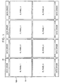
- FIG. 1 is a block diagram of an organic light emitting display (OLED) device using a tiling technique according to an exemplary embodiment of the present invention
- FIG. 2 is a detailed block diagram of an OLED array shown in FIG. 1 ;
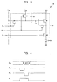
- FIG. 3 is a circuit diagram of a pixel of a pixel portion shown in FIG. 2 ;
- FIG. 4 is a timing diagram illustrating the operation of a pixel circuit shown in FIG. 3 ;
- FIG. 5 is a block diagram of an emission control driver of an organic EL panel according to the exemplary embodiment of the present invention.
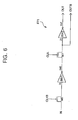
- FIG. 6 is a circuit diagram of a flip-flop of a shift register of the emission control driver shown in FIG. 5 ;
- FIG. 7 is a detailed circuit diagram of an inverter of the flip-flop shown in FIG. 6 ;
- FIG. 8 is a detailed circuit diagram of a logic gate of a logical operation portion of the emission control driver shown in FIG. 5 ;
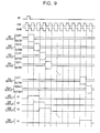
- FIG. 9 is a timing diagram illustrating the operation of an emission control driver according to the exemplary embodiment of the present invention. DETAILED DESCRIPTION OF THE ILLUSTRATED EMBODIMENTS
- FIG. 1 is a block diagram of an organic light emitting display (OLED) device using a tiling technique according to an exemplary embodiment of the present invention.
- OLED organic light emitting display
- the OLED device which may be designed to various sizes, is formed by bonding a plurality of OLED arrays 100.
- FIG. 1 illustrates eight OLED arrays 100, which are disposed in two rows and four columns and are bonded to one another.
- Each of the OLED arrays 100 includes an electroluminescent (EL) panel 10, which displays a predetermined image, and a data driver 20, which supplies a data signal to the EL panel 10.
- EL electroluminescent
- the EL panels 10 each have a similar construction.
- the edges of the EL panels 10 are bonded to one another using an adhesive to form a combined EL panel.
- the adhesive may be an ultraviolet (UV)-curing resin or a thermal curing resin, for example, an epoxy resin.
- Each of the EL panels 10 may be produced by the same fabricating process used for the production of an EL panel of a conventional OLED array. Accordingly, a large-sized EL panel may be fabricated by bonding a plurality of EL panels that are produced by the same fabricating process.
- Each of the EL panels 10, as shown in FIG. 2 includes a scan driver (14); an emission control driver (16); and a plurality of pixels (18).
- Each of the drivers and pixels includes a thin film transistor (TFT) which has a polysilicon channel in order to obtain fast response speed and high uniformity.
- TFT thin film transistor
- the polysilicon channel may be formed by forming an amorphous silicon (a-Si) layer on a glass substrate and crystallizing the a-Si layer using a low temperature polysilicon (LTPS) process.
- a plurality of polysilicon TFTs may be formed using the LTPS process. Thereafter, the pixel portion, the scan driver, and the emission control driver may be formed using the transistors in each of the EL panels 10.
- the pixel portion is comprised of red (R), green (G), and blue (B) sub-pixels, and the scan and emission control drivers select respective pixels and generate signals for controlling an emission operation of the selected respective pixels.
- R red
- G green
- B blue
- Each data driver 20, as shown in FIG. 2 is designed as an external integrated circuit (IC) using complementary metal oxide semiconductor (CMOS) technology and electrically connected to the corresponding EL panel 10.
- the EL panel 10 is electrically connected to the data driver 20 using a metal pattern that is printed on a flexible film. That is, an output terminal of the data driver 20 is electrically connected to one end of the metal pattern, and a data line disposed on the EL panel 10 is electrically connected to the other end thereof. This method is referred to as a tape carrier package (TCP) technique.
- TCP tape carrier package
- Each of the data drivers 20 transmits a data signal to the pixel portion of the EL panel 10 through a plurality of conductive lines that are disposed on the flexible film.
- FIG. 2 is a detailed block diagram of the OLED array shown in FIG. 1 .
- the OLED array 100 includes an EL panel 10 and a data driver 20.
- the EL panel 10 includes a pixel portion 12, a scan driver 14, and an emission control driver 16.
- the pixel portion 12 includes a plurality of data lines D 1 -D m , a plurality of scan lines S 1 -S n , a plurality of emission control lines E 1 -E n , and a plurality of pixel circuits P 11 -P nm (18), that are formed in regions where the data lines D 1 -D m , the scan lines S 1 -S n , and the emission control lines E 1 -E n intersect one another.
- the data lines D 1 -D m are electrically connected to the data driver 20 and extend in a vertical direction.
- the data lines D 1 -D m transmit data signals to the respective pixels P 11 -P nm .
- the scan lines S 1 -S n and the emission control lines E 1 -E n extend in the same direction as the data lines D 1 -D m (i.e., in the vertical direction).
- each of the scan S 1 -S n and emission E 1 -E n control lines and includes a contact hole in order to transmit the same scan and emission control signals to the pixels arranged in a horizontal direction. Therefore, metal interconnections, which contact the scan S 1 -S n and emission E 1 1-E n control lines through the contact holes, extend in a horizontal direction so that scan and emission control signals are transmitted to the pixels arranged in the horizontal direction.
- Each of the pixels P 11 -P nm includes R, G, and B sub-pixels that are repeatedly arranged in rows and columns.
- the R, G, and B sub-pixels used for an organic emission layer to emit light are formed from different organic materials, but are otherwise similar to one another with respect to the interconnection layout and circuit connection of their respective driving circuits. Accordingly, each of the pixels P 11 -P nm emits R, G, or B light with luminance corresponding to a data signal applied thereto and combines the R, G, and B light to display a specific color.
- the circuit construction of each of the pixels P 11 -P nm will be described with reference to FIG. 3 and FIG. 4 .
- FIG. 3 is a circuit diagram for one of the pixels P 11 -P nm of the pixel portion shown in FIG. 2 .
- a pixel circuit 18 includes a pixel driver 19 and an organic light emitting diode OLED.
- the pixel driver 19 is connected to a data line D m , a previous scan line S n-1 , a current scan line S n , an emission control line E n , a first power supply voltage line VDD, and a second power supply voltage line V SUS .
- the pixel driver 19 receives a data signal V DATA from the data line D m and supplies a driving current I OLED corresponding to the data signal V DATA to the organic light emitting diode OLED.
- the organic light emitting diode OLED includes an anode electrode, a cathode electrode, and an organic emission layer.
- the anode electrode is connected to the pixel driver 19, and the cathode electrode is connected to a reference power supply voltage line VSS.
- the organic light emitting diode OLED receives the driving current from the pixel driver 19 and emits light at a luminance corresponding to the amount of driving current I OLED .
- the pixel driver 19 includes five transistors M1-M5 and two capacitors C st and C vth . The configuration of the pixel driver 19 will now be described.
- the switching transistor M4 has a source terminal connected to the data line D m , and a gate terminal connected to the current scan line S n .
- the switching transistor M4 is turned on in response to a scan signal applied from the scan line S n and transmits the data signal V DATA applied from the data line D m .
- the driving transistor M1 has a source terminal connected to the first power supply voltage line VDD and generates a driving current I OLED corresponding to a voltage applied to a gate terminal thereof.
- the threshold voltage compensation transistor M2 is connected between the gate terminal and a drain terminal of the driving transistor M1.
- the threshold voltage compensation transistor M2 is turned on in response to a previous scan signal transmitted via the previous scan line S n-1 , and compensates a threshold voltage V TH of the driving transistor M1.
- the first capacitor C vth is connected between a drain terminal of the switching transistor M4 and the gate terminal of the driving transistor M1.
- the first capacitor C vth stores a voltage corresponding to the threshold voltage V TH of the driving transistor M1.
- the second capacitor C st is connected between the first power supply voltage line VDD and one terminal of the first capacitor C vth and stores a data voltage V DATA transmitted from the data line D m .
- the second power supply voltage application transistor M3 has a source terminal connected to the second power supply voltage line V SUS , and a drain terminal connected to a connection point between the first and second capacitors C vth and C st .
- the second power supply voltage application transistor M3 is turned on in response to the previous scan signal S n-1 applied to a gate terminal thereof, thus the second power supply voltage V SUS is applied to the connection point between the first and second capacitors C vth and C st .
- the emission control transistor M5 is connected between the drain terminal of the driving transistor M1 and the anode electrode of the organic light emitting diode OLED.
- the emission control transistor M5 is turned on/off in response to an emission control signal E n applied to a gate terminal thereof, so that the driving current I OLED from the driving transistor M1 is supplied to the organic light emitting diode OLED or cut off.
- FIG. 4 is a timing diagram illustrating the operation of the pixel circuit shown in FIG. 3 .
- the threshold voltage compensation transistor M2 and the second power supply voltage application transistor M3 are turned on, and the other transistors M4 and M5 are turned off.
- the driving transistor M1 is diode-connected so that a voltage of VDD -
- the second power supply voltage application transistor M3 is turned on so that a voltage of V SUS is applied to the other electrode A of the first capacitor C vth . Accordingly, the first capacitor C vth stores a voltage difference of V SUS - VDD +
- a low-level current scan signal S n a high-level previous scan signal S n-1 , and a high-level emission control signal E n are applied to the pixel circuit 18, thus only the switching transistor M4 is turned on.
- the data voltage V DATA is transmitted from the data line D m through the switching transistor M4 to the other electrode A of the first capacitor C vth .
- the one electrode B of the first capacitor C vth also has the same voltage variation as the other electrode A thereof.
- a voltage applied to the one electrode B of the first capacitor C vth and the gate terminal of the driving transistor M1 is VDD -
- - ⁇ V VDD -
- a high-level previous scan signal S n-1 a high-level current scan signal S n , and a low-level emission control signal E n are applied to the pixel circuit 18, thus only the emission control transistor M5 is turned on.
- the driving current I OLED supplied from the driving transistor M1 can be expressed as shown in Equation 1:
- 2 k ⁇ Vdata - Vsus 2 ,
- V TH refers to an absolute value of a threshold voltage of the driving transistor M1
- k is a constant
- the pixel circuit 18 shown in FIG. 3 can compensate the threshold voltage V TH caused by the first power supply voltage VDD.
- the scan driver 14 is disposed between the data driver 20 and the pixel portion 12. Since a large-sized panel is formed by bonding a plurality of EL panels 10, the scan driver 14 should be formed on the same side as the data driver 20.
- the scan driver 14 is connected to a plurality of scan lines S 1 -S n .
- the scan driver 14 sequentially transmits scan signals to the pixel portion 12 and sequentially selects each of the pixels P 11 -P nm .
- the emission control driver 16 is disposed between the scan driver 14 and the pixel portion 12, and connected to a plurality of emission control lines E 1 -E n . Thus, the emission control driver 16 sequentially transmits emission control signals to the pixel portion 12 and controls an emission time of each of the pixels P 11 -P nm .
- the data driver 20 transmits a data signal to the pixel portion 12 of the EL panel 10 through a plurality of conductive lines disposed on the flexible film as described above.
- the OLED array 100 includes the EL panel 10 and the data driver 20, where the EL panel 10 includes the pixel portion 12, the scan driver 14, and the emission control driver 16.
- the structure and operation of the emission control driver 16 will be described in detail with reference to exemplary embodiments of the present invention.
- FIG. 5 is a block diagram of an emission control driver of an organic EL panel according to the exemplary embodiment of the present invention.
- the emission control driver 16 includes a shift register 17 and a logical operation portion 22.
- the shift register 17 is connected to a plurality of flip-flops FF1, FF2, FF3, FF4,...shifting an input signal by one clock cycle and outputting the shifted signal.
- the logical operation portion 22 includes a plurality of logic gates OR1, OR2, OR3,...which receive output signals from the adjacent flip-flops FF1, FF2, FF3, and FF4 and generate emission control signals through logical OR operations for the received signals.
- the first flip-flop FF1 receives a start pulse V SP , a clock signal V CLK , and an inverted clock signal V CLKB , samples the start pulse V SP at a falling edge of the clock signal V CLK and maintains the sampled signal for a clock cycle, and outputs an output signal OUT 1 and an inverted output signal OUTB1.
- the second flip-flop FF2 receives the output signal OUT1 of the first flip-flop FF1, the clock signal V CLK , and the inverted clock signal V CLKB , shifts the received signal for one cycle of the clock signal V CLK , samples the shifted signal at a falling edge of the next cycle of the clock signal V CLK and maintains the sampled signal for a clock cycle, and outputs an output signal OUT2 and an inverted output signal OUTB2.
- the flip-flops FF1, FF2, FF3, FF4,... may have the same construction, which will be described in detail later.
- the logical operation portion 22 includes a plurality of logic gates OR1, OR2, OR3,...each of which is connected to an emission control line and transmits an emission control signal to each of the pixels.
- the first logic gate OR1 receives the output signals OUT1 and OUTB1 from the first flip-flop FF1 and the output signals OUT2 and OUTB2 from the second flip-flop FF2.
- the first logic gate OR1 performs a logical OR operation on the output signals OUT1, OUTB1, OUT2, and OUTB2.
- the first logic gate OR1 of the present invention outputs a low-level emission control signal E 1 , only when the output signals OUT1 and OUT2 of the first and second flip-flops FF1 and FF2, respectively, are at low levels and the inverted output signals OUTB1 and OUTB2 of the first and second flip-flops FF1 and FF2, respectively, are at high levels; and outputs a high-level emission control signal E 1 in all other cases.
- the second logic gate OR2 receives the output signals OUT2 and OUTB2 of the second flip-flop FF2 and output signals OUT3 and OUTB3 of the third flip-flop FF3, performs the same logical OR operation as the first logic gate OR1, and outputs a second emission control signal E 2 .
- each of the third logic gate OR3 through an n-th logic gate ORn performs a logical OR operation for four input signals, and outputs each of emission control signals E 3 -E n .
- the logic gates OR1 through ORn may have the same construction, which will be described in detail later.
- the emission control driver of the present invention includes the shift register 17 and the logical operation portion 22, and a connection of the two flip-flops FF1 and FF2 adjacent to the shift register 17 with the single logic gate OR1 of the logical operation portion 22 is defined as a basic emission control driving circuit 16_1, which generates the emission control signal E 1 .
- a basic emission control driving circuit 16_1 which generates the emission control signal E 1 .
- FIG. 6 is a circuit diagram of a representative flip-flop (i.e., the first flip-flop FF1) of the shift register of the emission control driver shown in FIG. 5 .
- the flip-flop FF1 includes two switching transistors M6 and M7 and two inverters INV1 and INV2. More specifically, the flip-flop FF 1 is controlled by an inverted clock signal CLKB and includes the transistors M6 and M7 and the first and second inverters INV1 and INV2.
- the transistor M6 samples an input signal IN at a falling edge of the inverted clock signal CLKB, and the first inverter INV1 inverts an output signal of the transistor M6.
- the transistor M7 samples an output signal of the first inverter INV1 at a falling edge of a clock signal CLK, and the second inverter INV2 inverts an output signal of the transistor M7.
- the transistors M6 and M7 are positive channel metal oxide semiconductors (PMOS) transistors.
- the transistor M6 samples the input signal IN and transmits the sampled signal to the first inverter INV1.
- the transistor M7 is turned on, and the first inverter INV1 inverts the sampled signal and outputs the inverted signal.
- An output signal OUTB of the first inverter INV1 is transmitted from the transistor M7, inverted again by the second inverter INV2, and output as an output signal OUT.
- the flip-flop FF1 makes use of the input signal IN, the clock signal CLK, and the inverted clock signal CLKB to generate a desired output signal.
- the input signal OUTB 1 and output signal OUT 1 of the second inverter INV2 are input as two input signals of the foregoing logic gate OR1.
- the output signal OUT of the second inverter INV2 is input to the next flip-flop FF2, and the next flip-flop FF2 makes use of the input signal OUT1, the clock signal CLK, and the inverted clock signal CLKB shifted by a clock cycle, to generate a desired output signal OUT2 and OUTB2, and then OUT1, OUT2, OUTB1 and OUTB2 input as an input signal of the logic gate OR1. Accordingly, the input signals OUT1, OUT2, OUTB1 and OUTB2 of logic gate OR1 is selected from the flip-flop FF1 and FF2 without additional signals, so that power consumption may be reduced.
- FIG. 7 is a detailed circuit diagram of an inverter of the flip-flop shown in FIG. 6 .
- first and second inverters INV1 and INV2 have the same construction, only the construction of the first inverter INV1 will be described for convenience.
- the inverter INV1 includes three PMOS transistors M8, M9, and M10.
- the transistor M8 has a source terminal connected to a first power supply voltage VDD, a gate terminal connected to an output terminal of the transistor M6 of the flip-flop FF1, and a drain terminal connected to an output terminal "out".
- the output terminal "out” is connected to an input terminal of the transistor M7 of the flip-flop FF1. Accordingly, the transistor M8 is turned on/off in response to an input signal "in” transmitted from the transistor M6 and outputs the first power supply voltage VDD to the output terminal "out” or cuts off the first power supply voltage VDD.
- the first power supply voltage VDD is a positive power supply voltage, for example, 5 V.
- the transistor M9 has a source terminal connected to the drain terminal of the transistor M8 and the output terminal "out", and a drain terminal connected to a second power supply voltage VSS.
- the transistor M9 acts as an active load according to a voltage applied to a gate terminal thereof.
- the transistor M10 is connected between the gate and drain terminals of the transistor M9, has a gate terminal and a drain terminal, which are diode-connected, and controls a gate voltage of the transistor M9.
- the second power supply voltage VSS is a negative power supply voltage, for example, -7 V.
- the transistor M9 acts as an active load and always remains turned on according to a difference between a voltage applied to the source terminal and a voltage applied to the gate terminal.
- a channel width over a channel length W/L of the transistor M9 is smaller that that of the transistor M8. In this case, when the transistor M8 is turned on, turned-on resistance of the transistor M9 may be higher than that of the transistor M8.
- the inverter INV1 may further include a capacitor C gs , which is connected between the source and gate terminals of the transistor M9 and maintains a voltage V gs between the source and gate terminals of the transistor M9 when the transistor M10 is turned off.
- the flip-flop of the present invention can sample an input signal and output a desired output signal in response to variations in the levels of a clock signal CLK and an inverted clock signal CLKB.
- output signals OUT1, OUTB1, OUT2, and OUTB2 of the adjacent flip-flops FF1 and FF2 are transmitted to input terminals of the logic gate OR1.
- FIG. 8 is a detailed circuit diagram of one of a plurality of logic gates of the logical operation portion of the emission control driver shown in FIG. 5 .
- the logic gate includes an input portion 31, a first active load 32, an output transistor M18, and a second active load 33.
- the input portion 31 is turned on/off in response to two input signals IN1 and IN2.
- the first active load 32 has a transistor M13 which is connected to the input portion 31 and selectively diode-connected in response to two inverted input signals INB1 and INB2.
- the output transistor M18 receives an output signal of the input portion 31 and is turned on/off in response to the level of the input signal.
- the second active load 33 has a transistor M17 which is connected to the output transistor M18 and selectively diode-connected in response to the two input signals IN1 and IN2.
- the logic gate further includes a switching portion 34, a first capacitor C1, and a second capacitor C2.
- the switching portion 34 is turned on/off in response to the input signals IN1 and IN2 and turns off the transistor M13 when the input signals IN1 and IN2 are at low levels.
- the first capacitor C 1 maintains a voltage between a source terminal and a gate terminal of the transistor M13
- the second capacitor C2 maintains a voltage between a source terminal and a gate terminal of the transistor M17.
- the logic gate further includes a transistor M19 connected to both ends of the second capacitor C2.
- the transistor M19 is turned on/off in response to an output signal of the input portion 31 and turns off the transistor M17 when the output signal is at a high level.
- an input signal IN1 and an inverted input signal INB1 respectively correspond to an output signal OUT1 and an inverted output signal OUTB1 of the flip-flop FF
- an input signal IN2 and an inverted input signal INB2 respectively correspond to an output signal OUT2 and an inverted output signal OUTB2 of the flip-flop FF2.
- the input portion 31 includes a transistor M11 and a transistor M12.
- the transistor M11 is connected to a positive power supply voltage V POS and turned on/off according to the level of the input signal IN1.
- the transistor M12 is connected to the transistor M11 and turned on/off according to the level of the input signal IN2.
- the input portion 31 is turned on only when both the input signals IN1 and IN2 are at low levels and outputs the positive power supply voltage V POS , and turned off in all other cases.
- the first active load 32 includes a transistor M13 and a pair of transistors M15_1 and M15_2.
- the transistor M13 is connected between the transistor M12 and a negative power supply voltage V neg and diode-connected according to the level of the inverted input signals INB1 and INB2.
- Each of the transistors M15_1 and M15_2 is connected between a gate terminal and a drain terminal of the transistor M13 and turned on/off according to the level of the inverted input signals INB1 and INB2.
- the transistor M13 is diode-connected except in the case where both the input signals INB1 and INB2 are at high levels and applies a voltage corresponding to the sum of the negative power supply voltage V neg and a threshold voltage V THM13 to an output terminal of the input portion 31.
- the output transistor M18 is connected between the positive power supply voltage V POS and an emission control line E1 and has a gate terminal connected to output terminals of the input portion 31 and the first active load 32 so that it is turned on/off in response to a voltage applied to the gate terminal. Thus, when the voltage applied to the gate terminal is at a low level, the transistor M18 is turned on and transmits the positive power supply voltage V POS to the emission control line E1.
- the second active load 33 includes a transistor M17 and a pair of transistors M16_1 and M16_2.
- the transistor M17 is connected between the transistor M18 and the negative power supply voltage V neg and diode-connected according to the level of the input signals IN1 and IN2.
- Each of the transistors M16_1 and M16_2 is connected between a gate terminal and a drain terminal of the transistor M17 and turned on/off according to the level of the input signals IN1 and IN2.
- the transistor M17 is diode-connected and transmits a voltage corresponding to the sum of the negative power supply voltage V neg and absolute value of a threshold voltage V THM17 to the emission control line E1.
- the switching portion 34 includes two transistors M14_1 and M14_2, which are connected in series. Each of the transistors M14_1 and M14_2 is connected between the source and gate terminals of the transistor M13 of the first active load 32 and turned on/off in response to the input signals IN1 and IN2.
- the switching portion 34 drives a voltage difference V gsM13 between the source and gate terminals of the transistor M13 to 0 V so that the transistor M13 is turned off. Accordingly, when the input portion 31 is turned on, the flow of static current through the first active load 32 can be prevented.
- the transistor M19 is connected between the source and gate terminals of the transistor M17 of the second active load 33 and turned on/off in response to the output signal of the first input portion 31.
- the transistor M19 drives a voltage difference V gsM17 between the source and gate terminals of the transistor M17 to 0 V so that the transistor M17 is turned off. Accordingly, when the transistor M18 is turned on, the flow of static current through the second active load 33 can be prevented.
- all transistors of the logic gate are PMOS transistors. But, it would be apparent to those skilled in the art that all transistors of the logic gate may be negative channel metal oxide semiconductor (NMOS) transistors. That is, by replacing the PMOS transistors with NMOS transistors and changing the positive power supply voltage V POS to the negative power supply voltage V neg , a logic gate comprised of NMOS transistors may be designed.
- NMOS metal oxide semiconductor
- the emission control signal E1 is output from the above-described logic gate according to the levels of the input signals IN1 and IN2 and the inverted input signals INB1 and INB2 as will be explained now.
- both the transistors M11 and M12 of the input portion 31 are turned on, and both the transistors M14_1 and M14_2 of the switching portion 34 are also turned on. Also, both the transistors M16_1 and M16_2 of the second active load 33 are turned on. But, the transistors M15_1 and M15_2 of the first active load 32 are turned off.
- the positive power supply voltage V POS is transmitted from the input portion 31 to the gate terminals of the output transistor M18 and the transistor M19.
- the switching portion 34 is turned on and drives a source-gate voltage V gsM13 of the transistor M13 of the first active load 32 to 0 V.
- the transistor M13 is turned off, thus no static current flows in the first active load 32.
- the output transistor M18 and the transistor M19 to which the positive power supply voltages V POS are applied are turned off, and the transistor M17, which is diode-connected to the second active load 33, outputs an emission control signal at a low level corresponding to the sum of the negative power supply voltage V neg and absolute value of the threshold voltage V THM17 ⁇
- the logic gate is in the following state.
- any one of the transistors M11 and M12 of the input portion 31 is turned off, and any one of the transistors M14_1 and M14_2 of the switching portion 34 is also turned off. Also, any one of the transistors M16_1 and M16_2 of the second active load 33 is turned off. But, any one of the parallel-connected transistors M15_1 and M15_2 of the first active load 32 is turned on.
- the input portion 31 and the switching portion 34 are turned off, and the transistor M13 of the first active load 32 is diode-connected, thus a voltage at the gate terminal of the output transistor M18 is reduced to a low level corresponding to the sum of the negative power supply voltage V neg and absolute value of the threshold voltage V THM13 .
- the output transistor M18 to which a low-level voltage is applied is turned on and applies the positive power supply voltage V POS to the emission control line E1.
- the transistor M19 is turned on and drives the source-gate voltage V gsM17 of the transistor M17 of the second active load 33 to 0 V. Accordingly, the transistor M17 is turned off, thus no static current flows in the active load 33.
- a high-level signal that is equivalent to the positive power supply voltage V POS is output to the emission control line E1.
- the emission control signal E1 remains at a high level.
- the logic gate of the logical operation portion 18 receives four signals OUT1, OUTB1, OUT2, and OUTB2 output from the adjacent flip-flops FF1 and FF2 without any additional signal and controls the first and second active loads 32 and 33 of the logic gate using the signals OUT1, OUTB1, OUT2, and OUTB2. Also, the logic gate of the logical operation portion 18 receives the output signals OUT1 and OUT2 and can generate a desired emission control signal E1 by performing a logical OR operation on the received signals OUT1 and OUT2.
- FIG. 9 is a timing diagram illustrating the operation of an emission control driver according to the exemplary embodiment of the present invention.
- a shift register having a plurality of flip-flops FF1-FFn+1 commonly receives a clock signal CLK and an inverted clock signal CLKB, and receives an output signal of a previous flip-flop as an input signal.
- a first flip-flop FF1 when a first flip-flop FF1 receives a start pulse SP, it outputs a high-level output signal OUT1 and a low-level inverted output signal OUTB1 for a clock cycle on a falling edge of a first cycle of the clock signal CLK.
- a second flip-flop FF2 receives the output signal OUT1 of the first flip-flop FF1, it outputs a high-level output signal OUT2 and a low-level inverted output signal OUTB2 for a clock cycle on a falling edge of a second cycle of the clock signal CLK.
- an n+1-th flip-flop FFn+1 receives an output signal OUTn of an n-th flip-flop FFn, it outputs a high-level output signal OUTn+1 and a low-level inverted output signal OUTBn+1 for a clock cycle on a falling edge of an n+1-th cycle of the clock signal CLK.
- the shift register of the present invention outputs two signals OUT and OUTB that are shifted by one clock cycle.
- a logical operation portion having a plurality of logic gates OR1-ORn receives output signals of the flip-flops FF1-FFn+1, performs a logical OR operation on the received signals, and outputs an emission control signal.
- the first logic gate OR1 receives two output signals OUT1 and OUTB1 from the first flip-flop FF1 and two output signals OUT2 and OUTB2 from the second flip-flop FF2.
- the first logic gate OR1 outputs a low-level emission control signal E1, only when the first and second output signals OUT1 and OUT2 are at low levels and the first and second inverted output signals OUTB1 and OUTB2 are at high levels, and outputs a high-level emission control signal E 1 except for the above-described case.
- the second logic gate OR2 receives two output signals OUT2 and OUTB2 from the second flip-flop FF2 and two output signals OUT3 and OUTB3 from the third flip-flop FF3.
- the second logic gate OR2 outputs a low-level emission control signal E2, only when the second and third output signals OUT2 and OUT3 are at low levels and the second and third inverted output signals OUTB2 and OUTB3 are at high levels, and outputs a high-level emission control signal E2 except for the above-described case.
- the second emission control signal E2 is shifted by a clock cycle later than the first emission control signal E1 and output.
- an n-th logic gate ORn receives two output signals OUTn and OUTBn from the n-th flip-flop FFn and receives two output signals OUTn+1 and OUTBn+1 from the n+1-th flip-flop FFn+1.
- the n-th logic gate ORn outputs a low-level emission control signal En, only when the n-th and n+1-th output signals OUTn and OUTn+1 are at low levels and the n-th and n+1-th inverted output signals OUTBn and OUTBn+1 are at high levels, and outputs a high-level emission control signal En except for the above-described case.
- a system-on-panel (SOP)-type emission control driver for the OLED can be easily fabricated by directly forming a plurality of flip-flops and a plurality of logic gates within a panel using PMOS transistors.
- each of the logic gates makes use of four output signals of adjacent flip-flops as input signals without any additional signal, power consumption can be reduced.
- the present invention employs four-input logic gates so that static current generated by a low-level input signal can be cut off, thus reducing power consumption caused by leakage current.
- the present invention provides an optimal SOP-type emission control driver and an OLED device that can minimize power consumption.
Landscapes
- Engineering & Computer Science (AREA)
- Microelectronics & Electronic Packaging (AREA)
- Power Engineering (AREA)
- Physics & Mathematics (AREA)
- Computer Hardware Design (AREA)
- General Physics & Mathematics (AREA)
- Theoretical Computer Science (AREA)
- Control Of Indicators Other Than Cathode Ray Tubes (AREA)
- Electroluminescent Light Sources (AREA)
- Control Of El Displays (AREA)
- Shift Register Type Memory (AREA)
Claims (17)
- Dispositif d'affichage électroluminescent organique (OLED), comportant un panneau électroluminescent (10), ledit panneau électroluminescent comportant:une partie de pixels présentant une pluralité de pixels agencés de manière à afficher une image;un pilote de commande d'émission (16) agencé de manière à appliquer un signal d'émission pour commander une durée d'émission de chacun des pixels, ledit pilote de commande d'émission (16) étant caractérisé en ce qu'il comporte:un registre à décalage (17) comportant une pluralité de bascules bistables, dans lequel la première bascule bistable est apte à recevoir une impulsion de départ et les bascules bistables restantes sont chacune aptes à recevoir un signal de sortie d'une bascule bistable précédente, et chaque bascule bistable génère un signal de sortie et un signal de sortie inversé en synchronisation avec un signal d'horloge et un signal d'horloge inversé; etune partie d'opération logique (22) comportant une pluralité de grilles logiques, dans laquelle chacune des grilles logiques est apte à recevoir un dit premier signal de sortie et un dit premier signal de sortie inversé en provenance de l'une desdites deux bascules bistables adjacentes et à recevoir un dit second signal de sortie et un dit second signal de sortie inversé de l'autre des deux bascules bistables adjacentes, dans laquelle chaque dite grille logique est apte à commander une charge active localisée au sein de ladite grille logique, en utilisant les signaux de sortie reçus, de manière à empêcher le passage de courant statique dans ladite grille logique, et dans laquelle chaque dite grille logique est apte à générer en sortie un signal de commande d'émission par le biais d'une opération logique sur les premier et second signaux de sortie et signaux de sortie inversés, dans lequel un signal de commande d'émission de faible niveau est généré en sortie lorsque les première et seconde sorties sont à des niveaux bas et que les signaux de sortie inversés sont à des niveaux élevés, et un signal de commande d'émission de haut niveau est généré en sortie dans tous les autres cas.
- Dispositif selon la revendication 1, dans lequel chacune des bascules bistables comprend:un premier transistor (M6);un premier inverseur (INV1);un deuxième transistor (M7); etun second inverseur (INV2);dans lequel le premier transistor (M6) est apte à échantillonner un signal d'entrée sur un front de descente du signal d'horloge inversé; le premier inverseur (INV1) est apte à inverser un signal de sortie du premier transistor (M6); le deuxième transistor (M7) est apte à échantillonner un signal de sortie du premier inverseur (1NV1) sur un front de descente du signal d'horloge; et le second inverseur (INV2) est apte à inverser un signal de sortie du deuxième transistor (M7).
- Dispositif selon la revendication 2, dans lequel chacune des bascules bistables adjacentes est apte à transmettre le signal de sortie du deuxième transistor (M7) et un signal de sortie du second inverseur (INV2) à une grille logique correspondante.
- Dispositif selon la revendication 2 ou 3, dans lequel chacun des premier et second inverseurs comprend:un troisième transistor (M8) connecté entre une tension d'alimentation positive et une borne de sortie, et lequel est apte à se mettre sous tension/hors tension en réponse à un signal émis par l'un des premier et deuxième transistors (M6, M7) de la bascule bistable; etun quatrième transistor (M9) connecté entre une tension d'alimentation négative et la borne de sortie et qui est apte à commander la quantité de courant en fonction de l'opération de mise sous/hors tension du troisième transistor (M8).
- Dispositif selon la revendication 4, dans lequel chacun des premier et second inverseurs (INV1, INV2) comprend en outre:un cinquième transistor (M10) connecté entre une borne de grille et une borne de drain du quatrième transistor (M9) et connecté en diode pour commander une tension de grille du quatrième transistor (M9).
- Dispositif selon la revendication 5, dans lequel le troisième transistor (M8) présente une résistance d'enclenchement inférieure à celle du quatrième transistor (M9).
- Dispositif selon la revendication 6, dans lequel chacun des premier et second inverseurs comprend en outre:un condensateur (Cgs) connecté entre une borne source et la borne de grille du quatrième transistor (M9) et lequel est apte à maintenir une tension entre la borne source et la borne de grille du quatrième transistor (M9) lorsque le cinquième transistor (M10) est mis hors tension.
- Dispositif selon la revendication 7, dans lequel les premier à cinquième transistors (M6-M10) sont des transistors MOS à canal P (semi-conducteurs à oxyde de métal à canal positif, PMOS).
- Dispositif selon l'une quelconque des revendications précédentes, dans lequel chacune des grilles logiques comprend:une partie d'entrée (31) connectée à une première tension d'alimentation et laquelle est apte à se mettre sous/hors tension selon les niveaux des premier et second signaux de sortie desdites deux bascules bistables adjacentes respectives;une première charge active (32), laquelle inclut un sixième transistor (M13) connecté entre la partie d'entrée (31) et une seconde tension d'alimentation et sélectivement connecté en diode selon les niveaux des premier et second signaux de sortie inversés des deux bascules bistables adjacentes;un transistor de sortie (M18) connecté entre la première tension d'alimentation et une ligne de commande d'émission et lequel est apte à se mettre hors/sous tension selon le niveau d'un signal de sortie de l'une parmi la partie d'entrée (31) et la première charge active (32); etune seconde charge active (33), laquelle présente un septième transistor (M17) connecté entre la seconde tension d'alimentation et la ligne de commande d'émission et connecté en diode de manière sélective selon les niveaux des premier et second signaux de sortie des deux bascules bistables adjacentes.
- Dispositif selon la revendication 9, dans lequel chaque partie d'entrée (31) comporte:un huitième transistor (M11) connecté à la première tension d'alimentation et lequel est apte à se mettre hors/sous tension selon le niveau dudit premier signal de sortie respectif; etun neuvième transistor (M12) connecté en série au huitième transistor (M11) et lequel est apte à se mettre hors/sous tension selon le niveau dudit second signal de sortie respectif.
- Dispositif selon la revendication 10, dans lequel la première charge active comporte:un dixième transistor (M15_1) connecté entre une borne de grille et une borne de drain du sixième transistor (M13) et lequel est apte à se mettre hors/sous tension selon le niveau du premier signal de sortie inversé;une onzième transistor (M15_2) connecté en parallèle au dixième transistor (M15_1) et lequel est apte à se mettre hors/sous tension en réponse au niveau du second signal de sortie inversé;dans lequel l'agencement est tel que, lorsque les premier et second signaux de sortie inversés sont à des niveaux élevés, le flux de courant dans la première charge active (32) est coupé.
- Dispositif selon la revendication 11, dans lequel la seconde charge active (33) comporte:un douzième transistor (M16_1) connecté à une borne de grille du septième transistor (m17) et lequel est apte à se mettre hors/sous tension selon le niveau du premier signal de sortie; etun treizième transistor (M16_2) connecté en série au douzième transistor (M16_1) et lequel est apte à se mettre hors/sous tension selon le niveau du second signal de sortie;dans lequel l'agencement est tel que, lorsqu'au moins un des premier et second signaux de sortie est à un niveau élevé, le flux de courant dans la seconde charge active (33) est coupé.
- Dispositif selon la revendication 12, dans lequel chacune des grilles logiques comprend en outre une partie de commutation (34) comportant:une quatorzième transistor (M14_1) connecté à une borne source du sixième transistor (M13) et lequel est apte à se mettre hors/sous tension selon le niveau du premier signal de sortie;un quinzième transistor (M14_2) connecté en série au quatorzième transistor (M14_1) et lequel est apte à se mettre hors/sous tension selon le niveau du second signal de sortie;dans lequel l'agencement est tel que, lorsque les premier et second signaux de sortie sont à des niveaux faibles, la partie de commutation (34) met hors tension le premier transistor (M6), de sorte que le flux de courant dans la première charge active (32) est coupé.
- Pilote de dispositif selon l'une quelconque des revendications 9 à 13, dans lequel chacune des grilles logiques comprend en outre:un premier condensateur (C1) connecté entre la borne source et la borne de grille du sixième transistor (M13) et lequel est apte maintenir une tension entre la borne source et la borne de grille du sixième transistor (M13); etun second condensateur (C2) connecté entre une borne source et une borne de grille du septième transistor (M17) et lequel est apte à maintenir une tension entre la borne source et la borne de grille du septième transistor (M17).
- Dispositif selon la revendication 14, dans lequel chacune des grilles logiques comprend en outre un seizième transistor (M19) connecté aux deux extrémités du second condensateur (C2) et lequel est apte à se mettre sous/hors tension selon le niveau du signal de sortie de l'une parmi la partie d'entrée (31) et la première charge active (32).
- Dispositif selon la revendication 15, dans lequel les sixième à seizième transistors sont des transistors MOS à canal P (semi-conducteurs à oxyde de métal à canal positif, PMOS).
- Dispositif selon la revendication 16, dans lequel le dispositif OLED est fabriqué en combinant une pluralité desdites matrices OLED en faisant appel à une technique de juxtaposition pour afficher une image prédéterminé.
Applications Claiming Priority (2)
| Application Number | Priority Date | Filing Date | Title |
|---|---|---|---|
| KR1020050075429A KR100685833B1 (ko) | 2005-08-17 | 2005-08-17 | 발광제어 구동부 및 이를 포함하는 유기 전계발광 표시장치 |
| KR1020050075428A KR100624117B1 (ko) | 2005-08-17 | 2005-08-17 | 발광제어 구동부 및 이를 포함하는 유기 전계발광 표시장치 |
Publications (2)
| Publication Number | Publication Date |
|---|---|
| EP1755103A1 EP1755103A1 (fr) | 2007-02-21 |
| EP1755103B1 true EP1755103B1 (fr) | 2010-12-22 |
Family
ID=37198729
Family Applications (1)
| Application Number | Title | Priority Date | Filing Date |
|---|---|---|---|
| EP06254019A Not-in-force EP1755103B1 (fr) | 2005-08-17 | 2006-07-31 | Dispositif d'affichage électroluminescent organique ayant un dispositif de contrôle d'émission générant des signaux de contrôle d'émission |
Country Status (4)
| Country | Link |
|---|---|
| US (1) | US7623097B2 (fr) |
| EP (1) | EP1755103B1 (fr) |
| JP (1) | JP4789746B2 (fr) |
| DE (1) | DE602006019032D1 (fr) |
Cited By (1)
| Publication number | Priority date | Publication date | Assignee | Title |
|---|---|---|---|---|
| TWI639309B (zh) | 2008-06-17 | 2018-10-21 | 半導體能源研究所股份有限公司 | 驅動電路,顯示裝置以及電子設備 |
Families Citing this family (36)
| Publication number | Priority date | Publication date | Assignee | Title |
|---|---|---|---|---|
| JP4789369B2 (ja) | 2001-08-08 | 2011-10-12 | 株式会社半導体エネルギー研究所 | 表示装置及び電子機器 |
| KR100748359B1 (ko) * | 2006-08-08 | 2007-08-09 | 삼성에스디아이 주식회사 | 논리 게이트 및 이를 이용한 주사 구동부와 유기전계발광표시장치 |
| KR100748360B1 (ko) * | 2006-08-08 | 2007-08-09 | 삼성에스디아이 주식회사 | 논리 게이트 및 이를 이용한 주사 구동부와 유기전계발광표시장치 |
| KR100873076B1 (ko) * | 2007-03-14 | 2008-12-09 | 삼성모바일디스플레이주식회사 | 화소 및 이를 이용한 유기전계발광 표시장치 및 그의구동방법 |
| US20090154152A1 (en) * | 2007-12-07 | 2009-06-18 | David Hoch | System, method, and architecture for multicelled electroluminense panel |
| KR101259727B1 (ko) * | 2008-10-24 | 2013-04-30 | 가부시키가이샤 한도오따이 에네루기 켄큐쇼 | 반도체 장치 |
| KR101040855B1 (ko) * | 2009-01-29 | 2011-06-14 | 삼성모바일디스플레이주식회사 | 발광 제어선 구동부 및 이를 이용한 유기전계발광 표시장치 |
| WO2011010546A1 (fr) * | 2009-07-24 | 2011-01-27 | Semiconductor Energy Laboratory Co., Ltd. | Dispositif à semi-conducteurs |
| KR101101105B1 (ko) * | 2009-11-04 | 2012-01-03 | 삼성모바일디스플레이주식회사 | 발광제어선 구동부 및 이를 이용한 유기전계발광 표시장치 |
| KR101049809B1 (ko) * | 2010-01-21 | 2011-07-15 | 삼성모바일디스플레이주식회사 | 표시 장치 및 그 구동 방법 |
| CN101826281B (zh) * | 2010-04-12 | 2013-04-17 | 杨忠义 | Oled-led智能平板显示与照明装置 |
| TWI421835B (zh) | 2010-05-10 | 2014-01-01 | Au Optronics Corp | 有機發光顯示器及其驅動方法 |
| KR101213494B1 (ko) * | 2010-05-12 | 2012-12-20 | 삼성디스플레이 주식회사 | 입체형 표시장치, 플렉서블 표시장치 및 상기 표시장치들의 제조방법 |
| CN101916533B (zh) * | 2010-05-19 | 2013-04-17 | 友达光电股份有限公司 | 有机发光显示器及其驱动方法 |
| KR101778701B1 (ko) * | 2010-08-11 | 2017-09-15 | 삼성디스플레이 주식회사 | 구동 장치 및 이를 포함하는 표시 장치 |
| KR101719187B1 (ko) * | 2010-09-14 | 2017-03-24 | 삼성디스플레이 주식회사 | 발광제어 구동부 및 그를 이용한 유기전계발광 표시장치 |
| KR101479297B1 (ko) * | 2010-09-14 | 2015-01-05 | 삼성디스플레이 주식회사 | 주사 구동부 및 그를 이용한 유기전계발광 표시장치 |
| KR101813192B1 (ko) * | 2011-05-31 | 2017-12-29 | 삼성디스플레이 주식회사 | 화소 및 이를 포함하는 표시장치, 및 그 구동방법 |
| CN102654974B (zh) | 2011-10-31 | 2015-01-21 | 京东方科技集团股份有限公司 | 一种像素单元驱动电路及其驱动方法、显示装置 |
| JP6075922B2 (ja) | 2012-02-29 | 2017-02-08 | 株式会社半導体エネルギー研究所 | 表示装置 |
| US9357149B2 (en) * | 2012-07-24 | 2016-05-31 | Forza Silicon Corporation | Stitched image sensor with multiple part drivers |
| KR101360767B1 (ko) * | 2012-08-17 | 2014-02-12 | 엘지디스플레이 주식회사 | 유기 발광 다이오드 표시장치 및 그 구동 방법 |
| KR101975581B1 (ko) | 2012-08-21 | 2019-09-11 | 삼성디스플레이 주식회사 | 발광 제어 구동부 및 그것을 포함하는 유기발광 표시장치 |
| KR102022519B1 (ko) * | 2013-05-13 | 2019-09-19 | 삼성디스플레이 주식회사 | 화소 및 이를 이용한 유기전계발광 표시장치 |
| KR102220825B1 (ko) * | 2013-09-05 | 2021-03-02 | 삼성전자주식회사 | 전자 장치와 전자 장치의 콘텐트 표시방법 |
| US9454935B2 (en) * | 2013-11-21 | 2016-09-27 | Lg Display Co., Ltd. | Organic light emitting diode display device |
| KR102471672B1 (ko) | 2015-11-13 | 2022-11-29 | 삼성전자주식회사 | 표시 제어 방법, 이를 구현한 디스플레이 패널, 디스플레이 장치 및 전자 장치 |
| KR102458968B1 (ko) | 2016-05-18 | 2022-10-27 | 삼성디스플레이 주식회사 | 표시장치 |
| CN109767720B (zh) * | 2019-03-27 | 2024-01-30 | 深圳市思坦科技有限公司 | 一种基于像素驱动的逻辑门运算电路、集成芯片和显示装置 |
| CN109920367B (zh) * | 2019-03-27 | 2024-01-30 | 深圳市思坦科技有限公司 | 一种基于像素驱动的逻辑门运算电路、集成芯片和显示装置 |
| CN109949741B (zh) * | 2019-03-27 | 2024-03-29 | 深圳市思坦科技有限公司 | 一种基于像素驱动的逻辑门运算电路、集成芯片和显示装置 |
| CN109785791B (zh) * | 2019-03-27 | 2024-01-30 | 深圳市思坦科技有限公司 | 一种基于像素驱动的逻辑门运算电路、集成芯片和显示装置 |
| CN110060639B (zh) | 2019-04-24 | 2021-07-06 | 深圳市华星光电半导体显示技术有限公司 | 阵列基板 |
| KR102767579B1 (ko) * | 2020-06-15 | 2025-02-17 | 삼성디스플레이 주식회사 | 표시 장치 |
| JP7697783B2 (ja) | 2020-12-23 | 2025-06-24 | 武漢天馬微電子有限公司 | 表示装置 |
| KR20250132574A (ko) * | 2024-02-28 | 2025-09-05 | 삼성디스플레이 주식회사 | 출력 제어 회로, 이를 포함하는 게이트 에미션 구동부 및 이를 포함하는 표시 장치 |
Family Cites Families (20)
| Publication number | Priority date | Publication date | Assignee | Title |
|---|---|---|---|---|
| JPS61211900A (ja) * | 1985-03-18 | 1986-09-19 | Nec Corp | 半導体集積回路 |
| US5093464A (en) * | 1988-12-01 | 1992-03-03 | Korea Institute Of Science And Technology | Wholly aromatic polyamide from N,N'-bis (4-amino phenyl)-isophthalamide |
| JPH02246097A (ja) * | 1989-03-17 | 1990-10-01 | Fujitsu Ltd | 半導体回路 |
| JPH05218814A (ja) * | 1992-01-31 | 1993-08-27 | Sony Corp | フリツプフロツプ回路 |
| JP3092506B2 (ja) * | 1995-03-27 | 2000-09-25 | カシオ計算機株式会社 | 半導体装置およびこれを用いた表示駆動装置 |
| JP2939865B2 (ja) * | 1995-07-03 | 1999-08-25 | カシオ計算機株式会社 | 薄膜半導体装置およびそれを用いた表示装置 |
| JP3063568B2 (ja) * | 1995-03-29 | 2000-07-12 | カシオ計算機株式会社 | 半導体装置およびこれを用いた表示駆動装置 |
| JPH0946216A (ja) * | 1995-07-28 | 1997-02-14 | Casio Comput Co Ltd | 半導体装置 |
| US6229506B1 (en) * | 1997-04-23 | 2001-05-08 | Sarnoff Corporation | Active matrix light emitting diode pixel structure and concomitant method |
| KR100327374B1 (ko) | 2000-03-06 | 2002-03-06 | 구자홍 | 액티브 구동 회로 |
| US7456810B2 (en) * | 2001-10-26 | 2008-11-25 | Semiconductor Energy Laboratory Co., Ltd. | Light-emitting device and driving method thereof |
| JP4391128B2 (ja) | 2002-05-30 | 2009-12-24 | シャープ株式会社 | 表示装置のドライバ回路およびシフトレジスタならびに表示装置 |
| KR100476368B1 (ko) * | 2002-11-05 | 2005-03-17 | 엘지.필립스 엘시디 주식회사 | 유기 전계발광 표시패널의 데이터 구동 장치 및 방법 |
| KR100502912B1 (ko) * | 2003-04-01 | 2005-07-21 | 삼성에스디아이 주식회사 | 발광 표시 장치 및 그 표시 패널과 구동 방법 |
| JP4232600B2 (ja) * | 2003-10-16 | 2009-03-04 | ソニー株式会社 | バッファ回路および表示装置 |
| KR100515305B1 (ko) * | 2003-10-29 | 2005-09-15 | 삼성에스디아이 주식회사 | 발광 표시 장치 및 그 표시 패널과 구동 방법 |
| JP4304293B2 (ja) * | 2003-11-12 | 2009-07-29 | 日本電気株式会社 | Gps測位システム、携帯端末装置、gps受信機及びそれらに用いる測位モード切替え方法 |
| KR100666549B1 (ko) * | 2003-11-27 | 2007-01-09 | 삼성에스디아이 주식회사 | 유기전계 발광표시장치 및 그의 구동방법 |
| KR100583519B1 (ko) | 2004-10-28 | 2006-05-25 | 삼성에스디아이 주식회사 | 주사 구동부 및 그를 이용한 발광표시장치 |
| KR100624317B1 (ko) * | 2004-12-24 | 2006-09-19 | 삼성에스디아이 주식회사 | 주사 구동부 및 이를 이용한 발광 표시장치와 그의 구동방법 |
-
2006
- 2006-07-13 US US11/457,198 patent/US7623097B2/en active Active
- 2006-07-31 EP EP06254019A patent/EP1755103B1/fr not_active Not-in-force
- 2006-07-31 DE DE602006019032T patent/DE602006019032D1/de active Active
- 2006-08-15 JP JP2006221420A patent/JP4789746B2/ja not_active Expired - Fee Related
Cited By (1)
| Publication number | Priority date | Publication date | Assignee | Title |
|---|---|---|---|---|
| TWI639309B (zh) | 2008-06-17 | 2018-10-21 | 半導體能源研究所股份有限公司 | 驅動電路,顯示裝置以及電子設備 |
Also Published As
| Publication number | Publication date |
|---|---|
| DE602006019032D1 (de) | 2011-02-03 |
| US20070040786A1 (en) | 2007-02-22 |
| JP2007052432A (ja) | 2007-03-01 |
| US7623097B2 (en) | 2009-11-24 |
| JP4789746B2 (ja) | 2011-10-12 |
| EP1755103A1 (fr) | 2007-02-21 |
Similar Documents
| Publication | Publication Date | Title |
|---|---|---|
| EP1755103B1 (fr) | Dispositif d'affichage électroluminescent organique ayant un dispositif de contrôle d'émission générant des signaux de contrôle d'émission | |
| US8264426B2 (en) | Organic light emitting display device and a method for generating scan signals for driving an organic light emitting display device having a scan driver | |
| KR100666637B1 (ko) | 유기 전계발광 표시장치의 발광제어 구동장치 | |
| US9959801B2 (en) | Display device and method for driving same with light-emission enable signal switching unit | |
| JP5301760B2 (ja) | 発光表示装置 | |
| CN113470556B (zh) | 显示装置 | |
| KR100528692B1 (ko) | 유기전계발광소자용 에이징 회로 및 그 구동방법 | |
| US20130027374A1 (en) | Electric current driving type display device and pixel circuit | |
| KR20100054729A (ko) | 액정 표시 장치 | |
| KR20210080781A (ko) | 게이트 드라이버 및 이를 포함하는 표시 장치 | |
| JP5089876B2 (ja) | 発光表示装置 | |
| CN100394468C (zh) | 电致发光显示器及其驱动方法 | |
| CN114170970B (zh) | 扫描驱动器及包括扫描驱动器的有机发光显示设备 | |
| KR20210076761A (ko) | 게이트 드라이버 및 이를 포함하는 표시 장치 | |
| US8040297B2 (en) | Emission control driver and organic light emitting display having the same | |
| CN100514419C (zh) | 有机发光显示设备及其发射控制驱动器和逻辑或电路 | |
| KR100774911B1 (ko) | 일렉트로 루미네센스 표시장치 | |
| KR100685842B1 (ko) | 발광제어 구동장치 및 이를 포함하는 유기전계발광표시장치 | |
| KR100685833B1 (ko) | 발광제어 구동부 및 이를 포함하는 유기 전계발광 표시장치 | |
| US8648776B2 (en) | Display device, pixel circuit, and method for driving same | |
| KR102674856B1 (ko) | 게이트 구동회로 및 이를 포함하는 표시 장치 | |
| KR100624133B1 (ko) | 발광제어 구동장치 및 이를 포함하는 유기전계발광표시장치 | |
| KR100538331B1 (ko) | 일렉트로 루미네센스 표시장치 | |
| CN120564599A (zh) | 栅极驱动电路和包括该栅极驱动电路的显示装置 |
Legal Events
| Date | Code | Title | Description |
|---|---|---|---|
| PUAI | Public reference made under article 153(3) epc to a published international application that has entered the european phase |
Free format text: ORIGINAL CODE: 0009012 |
|
| 17P | Request for examination filed |
Effective date: 20060808 |
|
| AK | Designated contracting states |
Kind code of ref document: A1 Designated state(s): AT BE BG CH CY CZ DE DK EE ES FI FR GB GR HU IE IS IT LI LT LU LV MC NL PL PT RO SE SI SK TR |
|
| AX | Request for extension of the european patent |
Extension state: AL BA HR MK YU |
|
| 17Q | First examination report despatched |
Effective date: 20070914 |
|
| AKX | Designation fees paid |
Designated state(s): DE FR GB |
|
| RAP1 | Party data changed (applicant data changed or rights of an application transferred) |
Owner name: SAMSUNG MOBILE DISPLAY CO., LTD. |
|
| GRAP | Despatch of communication of intention to grant a patent |
Free format text: ORIGINAL CODE: EPIDOSNIGR1 |
|
| RTI1 | Title (correction) |
Free format text: ORGANIC LIGHT EMITTING DISPLAY DEVICE HAVING AN EMISSION CONTROL DRIVER FOR OUTPUTTING EMISSION CONTROL SIGNALS |
|
| GRAS | Grant fee paid |
Free format text: ORIGINAL CODE: EPIDOSNIGR3 |
|
| GRAA | (expected) grant |
Free format text: ORIGINAL CODE: 0009210 |
|
| AK | Designated contracting states |
Kind code of ref document: B1 Designated state(s): DE FR GB |
|
| REG | Reference to a national code |
Ref country code: GB Ref legal event code: FG4D |
|
| REF | Corresponds to: |
Ref document number: 602006019032 Country of ref document: DE Date of ref document: 20110203 Kind code of ref document: P |
|
| REG | Reference to a national code |
Ref country code: DE Ref legal event code: R096 Ref document number: 602006019032 Country of ref document: DE Effective date: 20110203 |
|
| PLBE | No opposition filed within time limit |
Free format text: ORIGINAL CODE: 0009261 |
|
| STAA | Information on the status of an ep patent application or granted ep patent |
Free format text: STATUS: NO OPPOSITION FILED WITHIN TIME LIMIT |
|
| 26N | No opposition filed |
Effective date: 20110923 |
|
| REG | Reference to a national code |
Ref country code: DE Ref legal event code: R097 Ref document number: 602006019032 Country of ref document: DE Effective date: 20110923 |
|
| REG | Reference to a national code |
Ref country code: FR Ref legal event code: TP Owner name: SAMSUNG DISPLAY CO., LTD., KR Effective date: 20121226 |
|
| REG | Reference to a national code |
Ref country code: GB Ref legal event code: 732E Free format text: REGISTERED BETWEEN 20130103 AND 20130109 |
|
| REG | Reference to a national code |
Ref country code: DE Ref legal event code: R082 Ref document number: 602006019032 Country of ref document: DE Representative=s name: GULDE HENGELHAUPT ZIEBIG & SCHNEIDER, DE |
|
| REG | Reference to a national code |
Ref country code: DE Ref legal event code: R081 Ref document number: 602006019032 Country of ref document: DE Owner name: SAMSUNG DISPLAY CO., LTD., KR Free format text: FORMER OWNER: SAMSUNG MOBILE DISPLAY CO. LTD., SUWON, KR Effective date: 20130201 Ref country code: DE Ref legal event code: R082 Ref document number: 602006019032 Country of ref document: DE Representative=s name: GULDE HENGELHAUPT ZIEBIG & SCHNEIDER, DE Effective date: 20130201 Ref country code: DE Ref legal event code: R081 Ref document number: 602006019032 Country of ref document: DE Owner name: SAMSUNG DISPLAY CO., LTD., YONGIN-CITY, KR Free format text: FORMER OWNER: SAMSUNG MOBILE DISPLAY CO. LTD., SUWON, GYEONGGI, KR Effective date: 20130201 Ref country code: DE Ref legal event code: R082 Ref document number: 602006019032 Country of ref document: DE Representative=s name: GULDE & PARTNER PATENT- UND RECHTSANWALTSKANZL, DE Effective date: 20130201 |
|
| REG | Reference to a national code |
Ref country code: FR Ref legal event code: PLFP Year of fee payment: 11 |
|
| PGFP | Annual fee paid to national office [announced via postgrant information from national office to epo] |
Ref country code: GB Payment date: 20160621 Year of fee payment: 11 |
|
| PGFP | Annual fee paid to national office [announced via postgrant information from national office to epo] |
Ref country code: FR Payment date: 20160622 Year of fee payment: 11 |
|
| PGFP | Annual fee paid to national office [announced via postgrant information from national office to epo] |
Ref country code: DE Payment date: 20160621 Year of fee payment: 11 |
|
| REG | Reference to a national code |
Ref country code: DE Ref legal event code: R119 Ref document number: 602006019032 Country of ref document: DE |
|
| GBPC | Gb: european patent ceased through non-payment of renewal fee |
Effective date: 20170731 |
|
| REG | Reference to a national code |
Ref country code: FR Ref legal event code: ST Effective date: 20180330 |
|
| PG25 | Lapsed in a contracting state [announced via postgrant information from national office to epo] |
Ref country code: GB Free format text: LAPSE BECAUSE OF NON-PAYMENT OF DUE FEES Effective date: 20170731 Ref country code: DE Free format text: LAPSE BECAUSE OF NON-PAYMENT OF DUE FEES Effective date: 20180201 |
|
| PG25 | Lapsed in a contracting state [announced via postgrant information from national office to epo] |
Ref country code: FR Free format text: LAPSE BECAUSE OF NON-PAYMENT OF DUE FEES Effective date: 20170731 |