EP1758248A1 - Circuit et procédé de filtrage d'un signal radiofréquence - Google Patents
Circuit et procédé de filtrage d'un signal radiofréquence Download PDFInfo
- Publication number
- EP1758248A1 EP1758248A1 EP05018188A EP05018188A EP1758248A1 EP 1758248 A1 EP1758248 A1 EP 1758248A1 EP 05018188 A EP05018188 A EP 05018188A EP 05018188 A EP05018188 A EP 05018188A EP 1758248 A1 EP1758248 A1 EP 1758248A1
- Authority
- EP
- European Patent Office
- Prior art keywords
- circuit
- radio frequency
- active
- input terminal
- frequency signal
- Prior art date
- Legal status (The legal status is an assumption and is not a legal conclusion. Google has not performed a legal analysis and makes no representation as to the accuracy of the status listed.)
- Granted
Links
- 238000001914 filtration Methods 0.000 title claims abstract description 12
- 238000000034 method Methods 0.000 title claims description 6
- 239000003990 capacitor Substances 0.000 claims description 5
- 230000000903 blocking effect Effects 0.000 claims description 3
- 230000002238 attenuated effect Effects 0.000 claims description 2
- 230000005540 biological transmission Effects 0.000 description 1
- 230000001413 cellular effect Effects 0.000 description 1
- 238000004519 manufacturing process Methods 0.000 description 1
- 238000004088 simulation Methods 0.000 description 1
Images



Classifications
-
- H—ELECTRICITY
- H03—ELECTRONIC CIRCUITRY
- H03H—IMPEDANCE NETWORKS, e.g. RESONANT CIRCUITS; RESONATORS
- H03H11/00—Networks using active elements
- H03H11/02—Multiple-port networks
- H03H11/04—Frequency selective two-port networks
-
- H—ELECTRICITY
- H03—ELECTRONIC CIRCUITRY
- H03H—IMPEDANCE NETWORKS, e.g. RESONANT CIRCUITS; RESONATORS
- H03H7/00—Multiple-port networks comprising only passive electrical elements as network components
- H03H7/01—Frequency selective two-port networks
-
- H—ELECTRICITY
- H03—ELECTRONIC CIRCUITRY
- H03H—IMPEDANCE NETWORKS, e.g. RESONANT CIRCUITS; RESONATORS
- H03H7/00—Multiple-port networks comprising only passive electrical elements as network components
- H03H7/01—Frequency selective two-port networks
- H03H7/17—Structural details of sub-circuits of frequency selective networks
- H03H7/1741—Comprising typical LC combinations, irrespective of presence and location of additional resistors
- H03H7/1775—Parallel LC in shunt or branch path
-
- H—ELECTRICITY
- H03—ELECTRONIC CIRCUITRY
- H03H—IMPEDANCE NETWORKS, e.g. RESONANT CIRCUITS; RESONATORS
- H03H7/00—Multiple-port networks comprising only passive electrical elements as network components
- H03H7/01—Frequency selective two-port networks
- H03H7/17—Structural details of sub-circuits of frequency selective networks
- H03H7/1741—Comprising typical LC combinations, irrespective of presence and location of additional resistors
- H03H7/1791—Combined LC in shunt or branch path
Definitions
- the present invention generally relates to filters for radio frequency (RF) signals.
- Various kinds of active and passive RF and microwave filters are used in telecommunications devices to reject out-of-band signals, filter undesired harmonics and spurious components from signals prior to transmission and for performing various other functions within the telecommunications devices.
- GSM Group Switched Mobile
- DCS Digital Cellular System
- WLAN wireless local area network
- WPAN wireless personal area network
- the filter may be dispensed with, and instead a signal source having high linearity is provided so that the signal quality, i.e. the attenuation of the second harmonic, is sufficiently good without any kind of filtration.
- a signal source having high linearity is provided so that the signal quality, i.e. the attenuation of the second harmonic, is sufficiently good without any kind of filtration.
- Still further objectives of the present invention are to provide a filter, which is accurate, precise, straightforward to design and implement, and of low cost.
- a still further objective of the invention is to provide a method for filtering a radio frequency signal by means of a filter that fulfills the above objectives.
- a circuit for filtering a radio frequency signal comprise according to the present invention an input terminal, a filter device, an active AC shunt circuit and an output terminal.
- the input terminal is connected to the filter device and to a first input terminal of the shunt circuit.
- the filter device is connected to a second input terminal of the shunt circuit, and is provided for attenuating or blocking the radio frequency signal at a given frequency to the second input terminal of the shunt circuit.
- the shunt circuit is provided for shunting a signal at a frequency other than the given frequency as contained in the radio frequency signal to ground (e.g. a second harmonic of the radio frequency signal at the given frequency), and for outputting the radio frequency signal as filtered at the output terminal.
- a filter circuit which is highly efficient and which occupies small space.
- An attenuation of a second harmonic at 4.9 GHz of about 50 dB is achievable.
- the simple and small structure allows for the fabrication of small transmitters and transceivers.
- the filter circuit is further easily ingratable with a power amplifier or other transmitter or transceiver circuitry on a single chip.
- the filter device comprises preferably one or two resonant circuits: one for blocking the radio frequency signal at the given frequency from reaching the shunt circuit and/or one connected between the shunt circuit and ground for allowing the radio frequency signal at the given frequency to be shunted to ground, while the signal at the frequency other than the given frequency is blocked and thus directed to the shunt circuit.
- Each of the resonant circuits is preferably an LC-based circuit.
- the shunt circuit which is known per se in the field of shunting AC noise to ground in voltage regulators, comprises preferably a transconductance or transimpedance amplifier and a load resistor.
- the first input terminal of the shunt circuit is connected to the load resistor, whereas the second input terminal of the shunt circuit is connected to the transconductance amplifier.
- the transconductance amplifier and the load resistor are interconnected at the output terminal.
- the filter circuit of the present invention is primarily, but not exclusively, intended for use in transmitters in narrow band applications such as WLAN and Bluetooth transmitters.
- a filter circuit 1 for filtering a radio frequency signal is shown in Fig. 1.
- the filter circuit 1 comprises an input terminal 3, a filter device 5, and an active AC shunt circuit 7 having first 7a and second 7b input terminals and an output terminal 7c, wherein the first input terminal 7a is connected to the input terminal 3 of the filter circuit 1 and the output terminal 7c coincides with the output terminal of the filter circuit 1.
- the filter device 5 comprises two resonant circuits 9, 11, of which one is a notch filter 9 and one is a band pass filter 11.
- the notch filter 9 is connected between the input terminal 3 and the second input terminal 7b of the active AC shunt circuit 7, and comprises a capacitor 13 and an inductor 15 connected in parallel.
- the band pass filter 11 is connected between the second input terminal 7b of the active AC shunt circuit 7 and ground G, and comprises a capacitor 17 and an inductor 19 connected in series.
- the active AC shunt circuit 7 comprises a transconductance or transimpedance amplifier 21 and a resistor 23, wherein the first input terminal 7a of the active AC shunt circuit 7 is connected to the resistor 23 and the second input terminal 7b of the active AC shunt circuit 7 is connected to a first input terminal 21a of the transconductance amplifier 21.
- a second input terminal 21b of the transconductance amplifier 21 is connected to ground G.
- the resistor is connected to an output terminal of the transconductance amplifier 21 at the output terminal 7c of the active AC shunt circuit 7.
- the active AC shunt circuit 7 is known in the art per se, see e.g. the article Finesse Voltage Regulator Noise, which was publically available on the Internet page http://www.wenzel.com/documents/finesse.html of Wenzel Associates Inc. on August 10, 2005. However, the circuit is here used as a voltage regulator for removing noise.
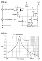
- An example implementation of an active AC shunt circuit 7 for use in the present invention is detailed in Fig. 5a.
- the operation of the filter circuit 1 is straightforward.
- the notch filter 9 blocks the radio frequency signal at a given or desired frequency, while other frequency components of the signal including the second harmonic are passed through.
- the band pass filter 11 allows the radio frequency signal at the given frequency to be shunted to ground G, while the other frequency components, including the second harmonic, are effectively blocked and directed towards the first input terminal 21a of the transconductance amplifier 21.
- the active AC shunt circuit 7 shunts the other frequency components of the signal, including the second harmonic, to ground G, and outputs at its output terminal 7c the radio frequency signal as filtered.
- the second harmonic current from the circuit may be calculated as V/R, where R is the resistance of the resistor 23. If a current-sink can be designed to sink this amount of second harmonic current to ground at the load, no second harmonic current will flow in the load.
- the required current sink is realized. The required transconductance is - 1/(R*V G ) where V G is the voltage gain in the resonant filter device 5 at the second harmonic frequency or whatever frequency component the circuit is designed to filter away.
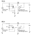
- Figs. 2-4 illustrate various modified circuits for filtering a radio frequency signal according to alternative embodiments of the invention, which differ from the embodiment in Fig. 1 regarding the filter device 5.
- the notch filter 9 is exchanged for a resistor 26
- the band pass filter 11 connected to ground G is exchanged for a resistor 31, and in the circuit of Fig. 3 the band pass filter has been removed in its entirety.
- the embodiments of Fig. 2-4 are simpler and smaller than the circuit if Fig. 1 they have also less capability of strong attenuation of e.g. the second harmonic.
- Figs. 5a-d illustrate an example implementation of the circuit of Fig. 1 together with simulated results.
- the circuit was connected to a signal source that transmitted 1.5 V DC, 10 mV AC at 2.45 GHz, and 1 mV AC at 4.90 GHz, the latter being referred to as the error signal.
- the error signal had 10 times lower amplitude than that of the signal at the desired frequency, 2.45 GHz.
- Values of the resistances, capacitances, and inductances are given in Fig. 5a.
- Figs. 5b and c show the filter response in dB at the nodes V(9) and V(6). From Fig. 5b it can be seen that the response was not flat outside of the blocked frequency. The gain of the transconductance amplifier had to be adjusted such that the filter attenuation obtained a maximum at the desired frequency, i.e. 2.45 GHz. From Fig. 5c it can be seen that the attenuation of the second harmonic by the filter circuit was about 50 dB, whereas the attenuation at the desired frequency was small.
- Fig. 5d shows the phase of the error signal and of the signal at the node V(9). As can bee seen the phase of the error signal and of the V(9) signal was very close, which made it possible to cancel out the error signal almost completely.
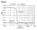
- Figs. 6a-c illustrate an example implementation of the circuit of Fig. 3 together with simulated results.
- the example implementation differs from the one of Fig. 5a in that the capacitor 17 and the inductor 19 as comprised in the band pass filter and a small resistor of 10 mohm are exchanged for a larger resistor of 200 ohm.
- Fig. 6b shows the filter response in dB at the node V(6) at the output terminal 7c of the filter circuit. It can be seen that the attenuation of the second harmonic by the filter circuit was about 25 dB, whereas the attenuation at the desired frequency was small.
- Fig. 6b shows the phase of the error signal and of the signal at the node V(9). The less optimum filtering was due to the phase difference as seen at 4.9 GHz. The filtering is less efficient by this example implementation, but may be still be acceptable as a compromise to reduce component cost and complexity of matching.
- the filter circuit 1 of the present invention may be provided in e.g. a radio transmitter, receiver, or transceiver or in a clock or oscillator circuit. It may be designed to filter widely or narrowly and strongly or weakly.
- the maximum attenuation was selected to be at the frequency of the second harmonic in the examples above. However, in other applications the maximum attenuation may be selected to be at another frequency or frequencies depending on the particular application.
Landscapes
- Networks Using Active Elements (AREA)
Priority Applications (4)
| Application Number | Priority Date | Filing Date | Title |
|---|---|---|---|
| DE602005014867T DE602005014867D1 (de) | 2005-08-22 | 2005-08-22 | Schaltung und Verfahren zur Filterung eines Radiofrequenzsignals |
| EP05018188A EP1758248B1 (fr) | 2005-08-22 | 2005-08-22 | Circuit et procédé de filtrage d'un signal radiofréquence |
| US11/507,949 US7436249B2 (en) | 2005-08-22 | 2006-08-22 | Circuit and method for filtering a radio frequency signal |
| CN200610121451.6A CN100533971C (zh) | 2005-08-22 | 2006-08-22 | 用于滤波射频信号的电路和方法 |
Applications Claiming Priority (1)
| Application Number | Priority Date | Filing Date | Title |
|---|---|---|---|
| EP05018188A EP1758248B1 (fr) | 2005-08-22 | 2005-08-22 | Circuit et procédé de filtrage d'un signal radiofréquence |
Publications (2)
| Publication Number | Publication Date |
|---|---|
| EP1758248A1 true EP1758248A1 (fr) | 2007-02-28 |
| EP1758248B1 EP1758248B1 (fr) | 2009-06-10 |
Family
ID=35521155
Family Applications (1)
| Application Number | Title | Priority Date | Filing Date |
|---|---|---|---|
| EP05018188A Expired - Lifetime EP1758248B1 (fr) | 2005-08-22 | 2005-08-22 | Circuit et procédé de filtrage d'un signal radiofréquence |
Country Status (4)
| Country | Link |
|---|---|
| US (1) | US7436249B2 (fr) |
| EP (1) | EP1758248B1 (fr) |
| CN (1) | CN100533971C (fr) |
| DE (1) | DE602005014867D1 (fr) |
Families Citing this family (5)
| Publication number | Priority date | Publication date | Assignee | Title |
|---|---|---|---|---|
| EP2621389B1 (fr) | 2010-10-01 | 2015-03-18 | Applied Medical Resources Corporation | Instrument électrochirurgical avec des mâchoires et avec une électrode |
| US8610495B2 (en) * | 2011-12-16 | 2013-12-17 | Intel Mobile Communications GmbH | Adaptive filtering of blocker signals in demodulators |
| TWI558098B (zh) * | 2014-09-01 | 2016-11-11 | 絡達科技股份有限公司 | 具有抑制射頻訊號干擾功能的音頻放大裝置 |
| US9331651B1 (en) * | 2014-12-30 | 2016-05-03 | Motorola Solutions, Inc. | Method and apparatus for automatic gain control in a current mode RF receiver |
| DE102015212845A1 (de) | 2015-07-09 | 2017-01-12 | Forschungszentrum Jülich GmbH | Filterschaltung zur Unterdrückung einer Signalverzerrung |
Citations (4)
| Publication number | Priority date | Publication date | Assignee | Title |
|---|---|---|---|---|
| US3564441A (en) * | 1968-03-04 | 1971-02-16 | United Control Corp | Low-pass active filter |
| US3849677A (en) * | 1973-06-26 | 1974-11-19 | Westinghouse Electric Corp | Hybrid power filters employing both active and passive elements |
| US4078205A (en) * | 1975-11-03 | 1978-03-07 | Sundstrand Data Control, Inc. | Electronic filter circuit |
| US5548165A (en) * | 1994-07-18 | 1996-08-20 | Regents Of The University Of Minnesota | Hybrid filter for reducing distortion in a power system |
Family Cites Families (1)
| Publication number | Priority date | Publication date | Assignee | Title |
|---|---|---|---|---|
| US4433315A (en) * | 1981-11-24 | 1984-02-21 | General Electric Company | Tunable coupling network |
-
2005
- 2005-08-22 EP EP05018188A patent/EP1758248B1/fr not_active Expired - Lifetime
- 2005-08-22 DE DE602005014867T patent/DE602005014867D1/de not_active Expired - Lifetime
-
2006
- 2006-08-22 CN CN200610121451.6A patent/CN100533971C/zh not_active Expired - Fee Related
- 2006-08-22 US US11/507,949 patent/US7436249B2/en active Active
Patent Citations (4)
| Publication number | Priority date | Publication date | Assignee | Title |
|---|---|---|---|---|
| US3564441A (en) * | 1968-03-04 | 1971-02-16 | United Control Corp | Low-pass active filter |
| US3849677A (en) * | 1973-06-26 | 1974-11-19 | Westinghouse Electric Corp | Hybrid power filters employing both active and passive elements |
| US4078205A (en) * | 1975-11-03 | 1978-03-07 | Sundstrand Data Control, Inc. | Electronic filter circuit |
| US5548165A (en) * | 1994-07-18 | 1996-08-20 | Regents Of The University Of Minnesota | Hybrid filter for reducing distortion in a power system |
Non-Patent Citations (2)
| Title |
|---|
| PENG F Z ET AL: "Harmonic sources and filtering approaches-series/parallel, active/passive, and their combined power filters", INDUSTRY APPLICATIONS CONFERENCE, 1999. THIRTY-FOURTH IAS ANNUAL MEETING. CONFERENCE RECORD OF THE 1999 IEEE PHOENIX, AZ, USA 3-7 OCT. 1999, PISCATAWAY, NJ, USA,IEEE, US, vol. 1, 3 October 1999 (1999-10-03), pages 448 - 455, XP010355186, ISBN: 0-7803-5589-X * |
| WENZEL ASSOCIATES, INC.: "Finesse Voltage Regulator Noise", WENZEL.COM, 16 June 2001 (2001-06-16), XP002364872, Retrieved from the Internet <URL:http://web.archive.org/web/20010616212658/www.wenzel.com/documents/finesse.html> [retrieved on 20060116] * |
Also Published As
| Publication number | Publication date |
|---|---|
| CN100533971C (zh) | 2009-08-26 |
| US7436249B2 (en) | 2008-10-14 |
| EP1758248B1 (fr) | 2009-06-10 |
| CN1921305A (zh) | 2007-02-28 |
| DE602005014867D1 (de) | 2009-07-23 |
| US20070054647A1 (en) | 2007-03-08 |
Similar Documents
| Publication | Publication Date | Title |
|---|---|---|
| US8786384B2 (en) | Self-matched band reject filter | |
| US9306535B2 (en) | Integrated receive filter including matched balun | |
| US10651821B2 (en) | Multiplexer, high-frequency front-end circuit, and communication apparatus | |
| US10951190B2 (en) | On-chip harmonic filtering for radio frequency (RF) communications | |
| US7466211B2 (en) | High-frequency switching module and frequency-characteristic adjusting method for high-frequency circuit | |
| KR20180094562A (ko) | 노치 필터링 내재화한 저잡음 증폭기 | |
| WO2017169645A1 (fr) | Circuit d'amplification de signal haute fréquence, module d'amplification de puissance, circuit frontal et dispositif de communication | |
| US10886895B2 (en) | Ladder-type frequency-variable filter, multiplexer, radio-frequency front end circuit, and communication terminal | |
| EP2485403A2 (fr) | Récepteur | |
| US20190081612A1 (en) | Signal Filtering Using Magnetic Coupling | |
| US20190149121A1 (en) | Multiplexer, radio-frequency front end circuit, and communication terminal | |
| US20200136590A1 (en) | Radio-frequency filter, multiplexer, radio-frequency front-end circuit, and communication device | |
| US20100164648A1 (en) | Innovative calibration circuit and method for high-frequency active filters | |
| US9419582B2 (en) | Filter device and duplexer | |
| US7436249B2 (en) | Circuit and method for filtering a radio frequency signal | |
| US9559735B2 (en) | Switching resonator filter circuits and methods | |
| US9130642B2 (en) | Frequency-selective circuit with mixer module implemented for controlling frequency response, and related signal processing apparatus and method | |
| US9124251B2 (en) | Two stage source-follower based filter | |
| CN111373657A (zh) | 放大电路、前端电路以及接收电路 | |
| US8391823B2 (en) | Signal processing apparatus having frequency-selective circuit with mixer module implemented for controlling frequency response and related method thereof | |
| US10027305B1 (en) | Filter including non-magnetic frequency selective limiters | |
| JP2021010062A (ja) | エクストラクタ | |
| KR100754549B1 (ko) | 무선 주파수 신호를 필터링하는 회로 및 방법 | |
| US20210135645A1 (en) | Multiplexer | |
| JP5807762B2 (ja) | 高周波モジュール及びそれを用いた携帯端末 |
Legal Events
| Date | Code | Title | Description |
|---|---|---|---|
| PUAI | Public reference made under article 153(3) epc to a published international application that has entered the european phase |
Free format text: ORIGINAL CODE: 0009012 |
|
| 17P | Request for examination filed |
Effective date: 20060719 |
|
| AK | Designated contracting states |
Kind code of ref document: A1 Designated state(s): AT BE BG CH CY CZ DE DK EE ES FI FR GB GR HU IE IS IT LI LT LU LV MC NL PL PT RO SE SI SK TR |
|
| AX | Request for extension of the european patent |
Extension state: AL BA HR MK YU |
|
| 17Q | First examination report despatched |
Effective date: 20070918 |
|
| AKX | Designation fees paid |
Designated state(s): DE FR GB |
|
| GRAP | Despatch of communication of intention to grant a patent |
Free format text: ORIGINAL CODE: EPIDOSNIGR1 |
|
| GRAS | Grant fee paid |
Free format text: ORIGINAL CODE: EPIDOSNIGR3 |
|
| GRAA | (expected) grant |
Free format text: ORIGINAL CODE: 0009210 |
|
| AK | Designated contracting states |
Kind code of ref document: B1 Designated state(s): DE FR GB |
|
| REG | Reference to a national code |
Ref country code: GB Ref legal event code: FG4D |
|
| REF | Corresponds to: |
Ref document number: 602005014867 Country of ref document: DE Date of ref document: 20090723 Kind code of ref document: P |
|
| PLBE | No opposition filed within time limit |
Free format text: ORIGINAL CODE: 0009261 |
|
| STAA | Information on the status of an ep patent application or granted ep patent |
Free format text: STATUS: NO OPPOSITION FILED WITHIN TIME LIMIT |
|
| 26N | No opposition filed |
Effective date: 20100311 |
|
| GBPC | Gb: european patent ceased through non-payment of renewal fee |
Effective date: 20090910 |
|
| PG25 | Lapsed in a contracting state [announced via postgrant information from national office to epo] |
Ref country code: GB Free format text: LAPSE BECAUSE OF NON-PAYMENT OF DUE FEES Effective date: 20090910 |
|
| REG | Reference to a national code |
Ref country code: FR Ref legal event code: PLFP Year of fee payment: 12 |
|
| REG | Reference to a national code |
Ref country code: FR Ref legal event code: PLFP Year of fee payment: 13 |
|
| REG | Reference to a national code |
Ref country code: FR Ref legal event code: PLFP Year of fee payment: 14 |
|
| PGFP | Annual fee paid to national office [announced via postgrant information from national office to epo] |
Ref country code: DE Payment date: 20201027 Year of fee payment: 16 |
|
| PGFP | Annual fee paid to national office [announced via postgrant information from national office to epo] |
Ref country code: FR Payment date: 20210819 Year of fee payment: 17 |
|
| REG | Reference to a national code |
Ref country code: DE Ref legal event code: R119 Ref document number: 602005014867 Country of ref document: DE |
|
| PG25 | Lapsed in a contracting state [announced via postgrant information from national office to epo] |
Ref country code: DE Free format text: LAPSE BECAUSE OF NON-PAYMENT OF DUE FEES Effective date: 20220301 |
|
| PG25 | Lapsed in a contracting state [announced via postgrant information from national office to epo] |
Ref country code: FR Free format text: LAPSE BECAUSE OF NON-PAYMENT OF DUE FEES Effective date: 20220831 |