EP1758438A2 - Herstellungsverfahren einer Leiterplatte - Google Patents
Herstellungsverfahren einer Leiterplatte Download PDFInfo
- Publication number
- EP1758438A2 EP1758438A2 EP06017783A EP06017783A EP1758438A2 EP 1758438 A2 EP1758438 A2 EP 1758438A2 EP 06017783 A EP06017783 A EP 06017783A EP 06017783 A EP06017783 A EP 06017783A EP 1758438 A2 EP1758438 A2 EP 1758438A2
- Authority
- EP
- European Patent Office
- Prior art keywords
- wiring
- layer
- insulating layer
- manufacturing
- wiring board
- Prior art date
- Legal status (The legal status is an assumption and is not a legal conclusion. Google has not performed a legal analysis and makes no representation as to the accuracy of the status listed.)
- Withdrawn
Links
Images






Classifications
-
- H—ELECTRICITY
- H05—ELECTRIC TECHNIQUES NOT OTHERWISE PROVIDED FOR
- H05K—PRINTED CIRCUITS; CASINGS OR CONSTRUCTIONAL DETAILS OF ELECTRIC APPARATUS; MANUFACTURE OF ASSEMBLAGES OF ELECTRICAL COMPONENTS
- H05K1/00—Printed circuits
- H05K1/18—Printed circuits structurally associated with non-printed electric components
- H05K1/182—Printed circuits structurally associated with non-printed electric components associated with components mounted in printed circuit boards [PCB], e.g. insert-mounted components [IMC]
- H05K1/185—Printed circuits structurally associated with non-printed electric components associated with components mounted in printed circuit boards [PCB], e.g. insert-mounted components [IMC] associated with components encapsulated in the insulating substrate of the PCBs; associated with components incorporated in internal layers of multilayer circuit boards
- H05K1/186—Printed circuits structurally associated with non-printed electric components associated with components mounted in printed circuit boards [PCB], e.g. insert-mounted components [IMC] associated with components encapsulated in the insulating substrate of the PCBs; associated with components incorporated in internal layers of multilayer circuit boards manufactured by mounting on or connecting to patterned circuits before or during embedding
-
- H—ELECTRICITY
- H05—ELECTRIC TECHNIQUES NOT OTHERWISE PROVIDED FOR
- H05K—PRINTED CIRCUITS; CASINGS OR CONSTRUCTIONAL DETAILS OF ELECTRIC APPARATUS; MANUFACTURE OF ASSEMBLAGES OF ELECTRICAL COMPONENTS
- H05K3/00—Apparatus or processes for manufacturing printed circuits
- H05K3/22—Secondary treatment of printed circuits
- H05K3/24—Reinforcing of the conductive pattern
-
- H—ELECTRICITY
- H10—SEMICONDUCTOR DEVICES; ELECTRIC SOLID-STATE DEVICES NOT OTHERWISE PROVIDED FOR
- H10P—GENERIC PROCESSES OR APPARATUS FOR THE MANUFACTURE OR TREATMENT OF DEVICES COVERED BY CLASS H10
- H10P72/00—Handling or holding of wafers, substrates or devices during manufacture or treatment thereof
- H10P72/70—Handling or holding of wafers, substrates or devices during manufacture or treatment thereof for supporting or gripping
- H10P72/74—Handling or holding of wafers, substrates or devices during manufacture or treatment thereof for supporting or gripping using temporarily an auxiliary support
-
- H—ELECTRICITY
- H10—SEMICONDUCTOR DEVICES; ELECTRIC SOLID-STATE DEVICES NOT OTHERWISE PROVIDED FOR
- H10W—GENERIC PACKAGES, INTERCONNECTIONS, CONNECTORS OR OTHER CONSTRUCTIONAL DETAILS OF DEVICES COVERED BY CLASS H10
- H10W70/00—Package substrates; Interposers; Redistribution layers [RDL]
- H10W70/01—Manufacture or treatment
- H10W70/05—Manufacture or treatment of insulating or insulated package substrates, or of interposers, or of redistribution layers
-
- H—ELECTRICITY
- H10—SEMICONDUCTOR DEVICES; ELECTRIC SOLID-STATE DEVICES NOT OTHERWISE PROVIDED FOR
- H10W—GENERIC PACKAGES, INTERCONNECTIONS, CONNECTORS OR OTHER CONSTRUCTIONAL DETAILS OF DEVICES COVERED BY CLASS H10
- H10W70/00—Package substrates; Interposers; Redistribution layers [RDL]
- H10W70/60—Insulating or insulated package substrates; Interposers; Redistribution layers
- H10W70/611—Insulating or insulated package substrates; Interposers; Redistribution layers for connecting multiple chips together
- H10W70/614—Insulating or insulated package substrates; Interposers; Redistribution layers for connecting multiple chips together the multiple chips being integrally enclosed
-
- H—ELECTRICITY
- H10—SEMICONDUCTOR DEVICES; ELECTRIC SOLID-STATE DEVICES NOT OTHERWISE PROVIDED FOR
- H10W—GENERIC PACKAGES, INTERCONNECTIONS, CONNECTORS OR OTHER CONSTRUCTIONAL DETAILS OF DEVICES COVERED BY CLASS H10
- H10W74/00—Encapsulations, e.g. protective coatings
- H10W74/01—Manufacture or treatment
- H10W74/012—Manufacture or treatment of encapsulations on active surfaces of flip-chip devices, e.g. forming underfills
-
- H—ELECTRICITY
- H10—SEMICONDUCTOR DEVICES; ELECTRIC SOLID-STATE DEVICES NOT OTHERWISE PROVIDED FOR
- H10W—GENERIC PACKAGES, INTERCONNECTIONS, CONNECTORS OR OTHER CONSTRUCTIONAL DETAILS OF DEVICES COVERED BY CLASS H10
- H10W74/00—Encapsulations, e.g. protective coatings
- H10W74/10—Encapsulations, e.g. protective coatings characterised by their shape or disposition
- H10W74/15—Encapsulations, e.g. protective coatings characterised by their shape or disposition on active surfaces of flip-chip devices, e.g. underfills
-
- H—ELECTRICITY
- H05—ELECTRIC TECHNIQUES NOT OTHERWISE PROVIDED FOR
- H05K—PRINTED CIRCUITS; CASINGS OR CONSTRUCTIONAL DETAILS OF ELECTRIC APPARATUS; MANUFACTURE OF ASSEMBLAGES OF ELECTRICAL COMPONENTS
- H05K2201/00—Indexing scheme relating to printed circuits covered by H05K1/00
- H05K2201/10—Details of components or other objects attached to or integrated in a printed circuit board
- H05K2201/10613—Details of electrical connections of non-printed components, e.g. special leads
- H05K2201/10621—Components characterised by their electrical contacts
- H05K2201/10674—Flip chip
-
- H—ELECTRICITY
- H05—ELECTRIC TECHNIQUES NOT OTHERWISE PROVIDED FOR
- H05K—PRINTED CIRCUITS; CASINGS OR CONSTRUCTIONAL DETAILS OF ELECTRIC APPARATUS; MANUFACTURE OF ASSEMBLAGES OF ELECTRICAL COMPONENTS
- H05K3/00—Apparatus or processes for manufacturing printed circuits
- H05K3/10—Apparatus or processes for manufacturing printed circuits in which conductive material is applied to the insulating support in such a manner as to form the desired conductive pattern
- H05K3/20—Apparatus or processes for manufacturing printed circuits in which conductive material is applied to the insulating support in such a manner as to form the desired conductive pattern by affixing prefabricated conductor pattern
-
- H—ELECTRICITY
- H05—ELECTRIC TECHNIQUES NOT OTHERWISE PROVIDED FOR
- H05K—PRINTED CIRCUITS; CASINGS OR CONSTRUCTIONAL DETAILS OF ELECTRIC APPARATUS; MANUFACTURE OF ASSEMBLAGES OF ELECTRICAL COMPONENTS
- H05K3/00—Apparatus or processes for manufacturing printed circuits
- H05K3/46—Manufacturing multilayer circuits
- H05K3/4644—Manufacturing multilayer circuits by building the multilayer layer by layer, i.e. build-up multilayer circuits
-
- H—ELECTRICITY
- H05—ELECTRIC TECHNIQUES NOT OTHERWISE PROVIDED FOR
- H05K—PRINTED CIRCUITS; CASINGS OR CONSTRUCTIONAL DETAILS OF ELECTRIC APPARATUS; MANUFACTURE OF ASSEMBLAGES OF ELECTRICAL COMPONENTS
- H05K3/00—Apparatus or processes for manufacturing printed circuits
- H05K3/46—Manufacturing multilayer circuits
- H05K3/4688—Composite multilayer circuits, i.e. comprising insulating layers having different properties
-
- H—ELECTRICITY
- H10—SEMICONDUCTOR DEVICES; ELECTRIC SOLID-STATE DEVICES NOT OTHERWISE PROVIDED FOR
- H10P—GENERIC PROCESSES OR APPARATUS FOR THE MANUFACTURE OR TREATMENT OF DEVICES COVERED BY CLASS H10
- H10P72/00—Handling or holding of wafers, substrates or devices during manufacture or treatment thereof
- H10P72/70—Handling or holding of wafers, substrates or devices during manufacture or treatment thereof for supporting or gripping
- H10P72/74—Handling or holding of wafers, substrates or devices during manufacture or treatment thereof for supporting or gripping using temporarily an auxiliary support
- H10P72/7424—Handling or holding of wafers, substrates or devices during manufacture or treatment thereof for supporting or gripping using temporarily an auxiliary support used as a support during the manufacture of self-supporting substrates
-
- H—ELECTRICITY
- H10—SEMICONDUCTOR DEVICES; ELECTRIC SOLID-STATE DEVICES NOT OTHERWISE PROVIDED FOR
- H10W—GENERIC PACKAGES, INTERCONNECTIONS, CONNECTORS OR OTHER CONSTRUCTIONAL DETAILS OF DEVICES COVERED BY CLASS H10
- H10W70/00—Package substrates; Interposers; Redistribution layers [RDL]
- H10W70/01—Manufacture or treatment
- H10W70/05—Manufacture or treatment of insulating or insulated package substrates, or of interposers, or of redistribution layers
- H10W70/093—Connecting or disconnecting other interconnections thereto or therefrom, e.g. connecting bond wires or bumps
-
- H—ELECTRICITY
- H10—SEMICONDUCTOR DEVICES; ELECTRIC SOLID-STATE DEVICES NOT OTHERWISE PROVIDED FOR
- H10W—GENERIC PACKAGES, INTERCONNECTIONS, CONNECTORS OR OTHER CONSTRUCTIONAL DETAILS OF DEVICES COVERED BY CLASS H10
- H10W70/00—Package substrates; Interposers; Redistribution layers [RDL]
- H10W70/60—Insulating or insulated package substrates; Interposers; Redistribution layers
- H10W70/62—Insulating or insulated package substrates; Interposers; Redistribution layers characterised by their interconnections
- H10W70/63—Vias, e.g. via plugs
-
- H—ELECTRICITY
- H10—SEMICONDUCTOR DEVICES; ELECTRIC SOLID-STATE DEVICES NOT OTHERWISE PROVIDED FOR
- H10W—GENERIC PACKAGES, INTERCONNECTIONS, CONNECTORS OR OTHER CONSTRUCTIONAL DETAILS OF DEVICES COVERED BY CLASS H10
- H10W72/00—Interconnections or connectors in packages
- H10W72/01—Manufacture or treatment
- H10W72/012—Manufacture or treatment of bump connectors, dummy bumps or thermal bumps
- H10W72/01221—Manufacture or treatment of bump connectors, dummy bumps or thermal bumps using local deposition
- H10W72/01225—Manufacture or treatment of bump connectors, dummy bumps or thermal bumps using local deposition in solid form, e.g. by using a powder or by stud bumping
-
- H—ELECTRICITY
- H10—SEMICONDUCTOR DEVICES; ELECTRIC SOLID-STATE DEVICES NOT OTHERWISE PROVIDED FOR
- H10W—GENERIC PACKAGES, INTERCONNECTIONS, CONNECTORS OR OTHER CONSTRUCTIONAL DETAILS OF DEVICES COVERED BY CLASS H10
- H10W72/00—Interconnections or connectors in packages
- H10W72/071—Connecting or disconnecting
- H10W72/072—Connecting or disconnecting of bump connectors
- H10W72/07202—Connecting or disconnecting of bump connectors using auxiliary members
- H10W72/07204—Connecting or disconnecting of bump connectors using auxiliary members using temporary auxiliary members, e.g. sacrificial coatings
-
- H—ELECTRICITY
- H10—SEMICONDUCTOR DEVICES; ELECTRIC SOLID-STATE DEVICES NOT OTHERWISE PROVIDED FOR
- H10W—GENERIC PACKAGES, INTERCONNECTIONS, CONNECTORS OR OTHER CONSTRUCTIONAL DETAILS OF DEVICES COVERED BY CLASS H10
- H10W72/00—Interconnections or connectors in packages
- H10W72/071—Connecting or disconnecting
- H10W72/072—Connecting or disconnecting of bump connectors
- H10W72/07231—Techniques
- H10W72/07236—Soldering or alloying
-
- H—ELECTRICITY
- H10—SEMICONDUCTOR DEVICES; ELECTRIC SOLID-STATE DEVICES NOT OTHERWISE PROVIDED FOR
- H10W—GENERIC PACKAGES, INTERCONNECTIONS, CONNECTORS OR OTHER CONSTRUCTIONAL DETAILS OF DEVICES COVERED BY CLASS H10
- H10W72/00—Interconnections or connectors in packages
- H10W72/071—Connecting or disconnecting
- H10W72/073—Connecting or disconnecting of die-attach connectors
- H10W72/07302—Connecting or disconnecting of die-attach connectors using an auxiliary member
- H10W72/07304—Connecting or disconnecting of die-attach connectors using an auxiliary member the auxiliary member being temporary, e.g. a sacrificial coating
-
- H—ELECTRICITY
- H10—SEMICONDUCTOR DEVICES; ELECTRIC SOLID-STATE DEVICES NOT OTHERWISE PROVIDED FOR
- H10W—GENERIC PACKAGES, INTERCONNECTIONS, CONNECTORS OR OTHER CONSTRUCTIONAL DETAILS OF DEVICES COVERED BY CLASS H10
- H10W72/00—Interconnections or connectors in packages
- H10W72/071—Connecting or disconnecting
- H10W72/075—Connecting or disconnecting of bond wires
-
- H—ELECTRICITY
- H10—SEMICONDUCTOR DEVICES; ELECTRIC SOLID-STATE DEVICES NOT OTHERWISE PROVIDED FOR
- H10W—GENERIC PACKAGES, INTERCONNECTIONS, CONNECTORS OR OTHER CONSTRUCTIONAL DETAILS OF DEVICES COVERED BY CLASS H10
- H10W72/00—Interconnections or connectors in packages
- H10W72/071—Connecting or disconnecting
- H10W72/077—Connecting of TAB connectors
-
- H—ELECTRICITY
- H10—SEMICONDUCTOR DEVICES; ELECTRIC SOLID-STATE DEVICES NOT OTHERWISE PROVIDED FOR
- H10W—GENERIC PACKAGES, INTERCONNECTIONS, CONNECTORS OR OTHER CONSTRUCTIONAL DETAILS OF DEVICES COVERED BY CLASS H10
- H10W72/00—Interconnections or connectors in packages
- H10W72/20—Bump connectors, e.g. solder bumps or copper pillars; Dummy bumps; Thermal bumps
- H10W72/251—Materials
- H10W72/252—Materials comprising solid metals or solid metalloids, e.g. PbSn, Ag or Cu
-
- H—ELECTRICITY
- H10—SEMICONDUCTOR DEVICES; ELECTRIC SOLID-STATE DEVICES NOT OTHERWISE PROVIDED FOR
- H10W—GENERIC PACKAGES, INTERCONNECTIONS, CONNECTORS OR OTHER CONSTRUCTIONAL DETAILS OF DEVICES COVERED BY CLASS H10
- H10W72/00—Interconnections or connectors in packages
- H10W72/851—Dispositions of multiple connectors or interconnections
- H10W72/853—On the same surface
- H10W72/856—Bump connectors and die-attach connectors
-
- H—ELECTRICITY
- H10—SEMICONDUCTOR DEVICES; ELECTRIC SOLID-STATE DEVICES NOT OTHERWISE PROVIDED FOR
- H10W—GENERIC PACKAGES, INTERCONNECTIONS, CONNECTORS OR OTHER CONSTRUCTIONAL DETAILS OF DEVICES COVERED BY CLASS H10
- H10W90/00—Package configurations
- H10W90/701—Package configurations characterised by the relative positions of pads or connectors relative to package parts
- H10W90/721—Package configurations characterised by the relative positions of pads or connectors relative to package parts of bump connectors
- H10W90/724—Package configurations characterised by the relative positions of pads or connectors relative to package parts of bump connectors between a chip and a stacked insulating package substrate, interposer or RDL
-
- H—ELECTRICITY
- H10—SEMICONDUCTOR DEVICES; ELECTRIC SOLID-STATE DEVICES NOT OTHERWISE PROVIDED FOR
- H10W—GENERIC PACKAGES, INTERCONNECTIONS, CONNECTORS OR OTHER CONSTRUCTIONAL DETAILS OF DEVICES COVERED BY CLASS H10
- H10W90/00—Package configurations
- H10W90/701—Package configurations characterised by the relative positions of pads or connectors relative to package parts
- H10W90/731—Package configurations characterised by the relative positions of pads or connectors relative to package parts of die-attach connectors
- H10W90/734—Package configurations characterised by the relative positions of pads or connectors relative to package parts of die-attach connectors between a chip and a stacked insulating package substrate, interposer or RDL
-
- Y—GENERAL TAGGING OF NEW TECHNOLOGICAL DEVELOPMENTS; GENERAL TAGGING OF CROSS-SECTIONAL TECHNOLOGIES SPANNING OVER SEVERAL SECTIONS OF THE IPC; TECHNICAL SUBJECTS COVERED BY FORMER USPC CROSS-REFERENCE ART COLLECTIONS [XRACs] AND DIGESTS
- Y10—TECHNICAL SUBJECTS COVERED BY FORMER USPC
- Y10T—TECHNICAL SUBJECTS COVERED BY FORMER US CLASSIFICATION
- Y10T29/00—Metal working
- Y10T29/49—Method of mechanical manufacture
- Y10T29/49002—Electrical device making
- Y10T29/49117—Conductor or circuit manufacturing
-
- Y—GENERAL TAGGING OF NEW TECHNOLOGICAL DEVELOPMENTS; GENERAL TAGGING OF CROSS-SECTIONAL TECHNOLOGIES SPANNING OVER SEVERAL SECTIONS OF THE IPC; TECHNICAL SUBJECTS COVERED BY FORMER USPC CROSS-REFERENCE ART COLLECTIONS [XRACs] AND DIGESTS
- Y10—TECHNICAL SUBJECTS COVERED BY FORMER USPC
- Y10T—TECHNICAL SUBJECTS COVERED BY FORMER US CLASSIFICATION
- Y10T29/00—Metal working
- Y10T29/49—Method of mechanical manufacture
- Y10T29/49002—Electrical device making
- Y10T29/49117—Conductor or circuit manufacturing
- Y10T29/49124—On flat or curved insulated base, e.g., printed circuit, etc.
- Y10T29/49126—Assembling bases
-
- Y—GENERAL TAGGING OF NEW TECHNOLOGICAL DEVELOPMENTS; GENERAL TAGGING OF CROSS-SECTIONAL TECHNOLOGIES SPANNING OVER SEVERAL SECTIONS OF THE IPC; TECHNICAL SUBJECTS COVERED BY FORMER USPC CROSS-REFERENCE ART COLLECTIONS [XRACs] AND DIGESTS
- Y10—TECHNICAL SUBJECTS COVERED BY FORMER USPC
- Y10T—TECHNICAL SUBJECTS COVERED BY FORMER US CLASSIFICATION
- Y10T29/00—Metal working
- Y10T29/49—Method of mechanical manufacture
- Y10T29/49002—Electrical device making
- Y10T29/49117—Conductor or circuit manufacturing
- Y10T29/49124—On flat or curved insulated base, e.g., printed circuit, etc.
- Y10T29/49128—Assembling formed circuit to base
-
- Y—GENERAL TAGGING OF NEW TECHNOLOGICAL DEVELOPMENTS; GENERAL TAGGING OF CROSS-SECTIONAL TECHNOLOGIES SPANNING OVER SEVERAL SECTIONS OF THE IPC; TECHNICAL SUBJECTS COVERED BY FORMER USPC CROSS-REFERENCE ART COLLECTIONS [XRACs] AND DIGESTS
- Y10—TECHNICAL SUBJECTS COVERED BY FORMER USPC
- Y10T—TECHNICAL SUBJECTS COVERED BY FORMER US CLASSIFICATION
- Y10T29/00—Metal working
- Y10T29/49—Method of mechanical manufacture
- Y10T29/49002—Electrical device making
- Y10T29/49117—Conductor or circuit manufacturing
- Y10T29/49124—On flat or curved insulated base, e.g., printed circuit, etc.
- Y10T29/4913—Assembling to base an electrical component, e.g., capacitor, etc.
-
- Y—GENERAL TAGGING OF NEW TECHNOLOGICAL DEVELOPMENTS; GENERAL TAGGING OF CROSS-SECTIONAL TECHNOLOGIES SPANNING OVER SEVERAL SECTIONS OF THE IPC; TECHNICAL SUBJECTS COVERED BY FORMER USPC CROSS-REFERENCE ART COLLECTIONS [XRACs] AND DIGESTS
- Y10—TECHNICAL SUBJECTS COVERED BY FORMER USPC
- Y10T—TECHNICAL SUBJECTS COVERED BY FORMER US CLASSIFICATION
- Y10T29/00—Metal working
- Y10T29/49—Method of mechanical manufacture
- Y10T29/49002—Electrical device making
- Y10T29/49117—Conductor or circuit manufacturing
- Y10T29/49124—On flat or curved insulated base, e.g., printed circuit, etc.
- Y10T29/4913—Assembling to base an electrical component, e.g., capacitor, etc.
- Y10T29/49133—Assembling to base an electrical component, e.g., capacitor, etc. with component orienting
- Y10T29/49135—Assembling to base an electrical component, e.g., capacitor, etc. with component orienting and shaping, e.g., cutting or bending, etc.
-
- Y—GENERAL TAGGING OF NEW TECHNOLOGICAL DEVELOPMENTS; GENERAL TAGGING OF CROSS-SECTIONAL TECHNOLOGIES SPANNING OVER SEVERAL SECTIONS OF THE IPC; TECHNICAL SUBJECTS COVERED BY FORMER USPC CROSS-REFERENCE ART COLLECTIONS [XRACs] AND DIGESTS
- Y10—TECHNICAL SUBJECTS COVERED BY FORMER USPC
- Y10T—TECHNICAL SUBJECTS COVERED BY FORMER US CLASSIFICATION
- Y10T29/00—Metal working
- Y10T29/49—Method of mechanical manufacture
- Y10T29/49002—Electrical device making
- Y10T29/49117—Conductor or circuit manufacturing
- Y10T29/49124—On flat or curved insulated base, e.g., printed circuit, etc.
- Y10T29/49147—Assembling terminal to base
- Y10T29/49149—Assembling terminal to base by metal fusion bonding
-
- Y—GENERAL TAGGING OF NEW TECHNOLOGICAL DEVELOPMENTS; GENERAL TAGGING OF CROSS-SECTIONAL TECHNOLOGIES SPANNING OVER SEVERAL SECTIONS OF THE IPC; TECHNICAL SUBJECTS COVERED BY FORMER USPC CROSS-REFERENCE ART COLLECTIONS [XRACs] AND DIGESTS
- Y10—TECHNICAL SUBJECTS COVERED BY FORMER USPC
- Y10T—TECHNICAL SUBJECTS COVERED BY FORMER US CLASSIFICATION
- Y10T29/00—Metal working
- Y10T29/49—Method of mechanical manufacture
- Y10T29/49002—Electrical device making
- Y10T29/49117—Conductor or circuit manufacturing
- Y10T29/49124—On flat or curved insulated base, e.g., printed circuit, etc.
- Y10T29/49155—Manufacturing circuit on or in base
-
- Y—GENERAL TAGGING OF NEW TECHNOLOGICAL DEVELOPMENTS; GENERAL TAGGING OF CROSS-SECTIONAL TECHNOLOGIES SPANNING OVER SEVERAL SECTIONS OF THE IPC; TECHNICAL SUBJECTS COVERED BY FORMER USPC CROSS-REFERENCE ART COLLECTIONS [XRACs] AND DIGESTS
- Y10—TECHNICAL SUBJECTS COVERED BY FORMER USPC
- Y10T—TECHNICAL SUBJECTS COVERED BY FORMER US CLASSIFICATION
- Y10T29/00—Metal working
- Y10T29/49—Method of mechanical manufacture
- Y10T29/49002—Electrical device making
- Y10T29/49117—Conductor or circuit manufacturing
- Y10T29/49124—On flat or curved insulated base, e.g., printed circuit, etc.
- Y10T29/49155—Manufacturing circuit on or in base
- Y10T29/49156—Manufacturing circuit on or in base with selective destruction of conductive paths
-
- Y—GENERAL TAGGING OF NEW TECHNOLOGICAL DEVELOPMENTS; GENERAL TAGGING OF CROSS-SECTIONAL TECHNOLOGIES SPANNING OVER SEVERAL SECTIONS OF THE IPC; TECHNICAL SUBJECTS COVERED BY FORMER USPC CROSS-REFERENCE ART COLLECTIONS [XRACs] AND DIGESTS
- Y10—TECHNICAL SUBJECTS COVERED BY FORMER USPC
- Y10T—TECHNICAL SUBJECTS COVERED BY FORMER US CLASSIFICATION
- Y10T29/00—Metal working
- Y10T29/53—Means to assemble or disassemble
- Y10T29/5313—Means to assemble electrical device
- Y10T29/53174—Means to fasten electrical component to wiring board, base, or substrate
Definitions
- the present invention relates to a method of manufacturing a wiring board, and in particular to a wiring board in which a semiconductor chip is incorporated.
- chip built-in wiring boards for example, refer to JP-A-2004-327624
- various structures designed to build a semiconductor chip in a substrate Such a chip built-in wiring board has wiring connected to a semiconductor chip and includes a connecting section formed thereon to connect the wiring board to another device, a mother board, etc.
- a possible warpage of a wiring board has presented a problem in a case where a chip built-in wiring board with a thinner design and higher packing density is to be provided.
- a structure is required where a board such as a core board having a predetermined thickness is laminated on a layer where a semiconductor chip is embedded for effective suppression of warpage.
- a laminated structure it is difficult to achieve a thinner design and higher density of a wiring board.
- the present invention has been made in view of the above circumstances, and provides a method of manufacturing an innovative and useful wiring board that solves the above problems.
- An object of an embodiment of the invention is to achieve a thinner chip-built-in wiring board as well as to suppress warpage of the wiring board.
- a method manufacturing a wiring board comprising:
- the supporting board is removed after the insulating layer where a semiconductor chip is embedded and the wiring connected to the semiconductor chip are formed, and the first and second reinforcing layers are simultaneously formed so as to sandwich the insulating layer and the like where the supporting board is absent.
- a reinforcing layer shows large shrinkage on curing.
- the shrinkage on curing is uniformly applied from above and below the insulating layer, thus preventing an occurrence of warpage.
- the reinforcing layer is made of a prepreg material.
- a prepreg material is used as a reinforcing layer. This makes it easy to form the reinforcing layer as well as enhance the rigidity of the reinforcing layer.
- the method of manufacturing a wiring board comprising:
- removal of a supporting board is stopped by the stop layer thus preventing removal of the supporting board from having an effect on the layers that are inside of the stop layer.
- Control of removal processing in removing the supporting board is made easy, and thus the manufacture of a wiring board is simplified.
- the method of manufacturing a wiring board comprising:
- the method of manufacturing a wiring board comprising:
- Embodiments according to the invention are also directed to apparatuses for carrying out the disclosed methods and including apparatus parts for performing each described method steps. These method steps may be performed by way of hardware components, a computer programmed by appropriate software, by any combination of the two or in any other manner. Furthermore, embodiments according to the invention are also directed to methods by which the described apparatus is manufactured. It includes method steps for carrying manufacturing every part of the apparatus. According to the method of the invention, it is possible to simultaneously form layers that are formed on and under the insulating layer, thus the manufacturing process is facilitated and time required for manufacture is reduced.
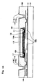
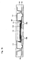
- Fig. 1 is a schematic cross-sectional view of a wiring board 100 manufactured by a method of manufacturing a wiring board as an embodiment of the invention.
- the structure of the wiring board 100 will be described before describing the method of manufacturing the wiring board 100.
- the wiring board 100 manufactured in this embodiment has an insulating layer 106 including a so-called buildup resin material such as epoxy where a semiconductor chip 110 is embedded.
- First and second reinforcing layers 103, 114 are formed with respect to the insulating layer 106.
- the reinforcing layers 103, 114 are arranged so as to sandwich the insulating layer 106 from top and bottom as shown in the figure.
- the reinforcing layers 103, 114 are formed using a material having a high rigidity such as a prepreg material.
- the insulating layer 106 is formed of a buildup resin material that is flexible as mentioned earlier. By providing reinforcing layers 103, 114 to sandwich the insulating layer 106, the insulating layer 106 is reinforced by the reinforcing layers 103, 114.
- the semiconductor chip 110 is connected to a wiring section (described later) and is connected to an electrode 102 formed in an opening in a solder resist 119 or an electrode 118 formed in an opening in a solder resist 117 via the wiring section.
- the electrode 102 or 118 is used for connection to a mother board, another device, or a connecting device, for example.
- a stud bump 111 composed of for example Au.
- the stud bump 111 is connected to a wiring section 108 embedded in the insulating layer 106 via a solder-connecting section 109, for example.
- an underfill layer 110A is formed from the viewpoint of protecting the stub bump 111 and suppressing generating of a stress.
- the wiring board 100 has wiring sections 105, 113, 116 as well as the wiring section 108.
- the wiring sections 105, 108, 113, 116 are formed of for example, Cu.
- the wiring section 105 includes a via plug 105a and pattern wiring 105b.
- the via plug 105a is formed at the opening formed in the reinforcing layer 103.
- pattern wiring 105b is formed on the reinforcing layer 103.
- the wiring section 108 is formed in the insulating layer 106.
- the wiring section 108 is formed above the wiring section 105 as shown in the figure.
- the wiring section 108 includes a via plug 108a formed on the pattern wiring 105b and a pattern wiring 108b connected to the via plug 108a.
- To the pattern wiring 108b is connected a semiconductor chip 110 via the solder-connecting section 109 and the stud bump 111 as described earlier.
- the wiring section 113 is formed in the insulating layer 106.
- the wiring section 113 is formed above the wiring section 108 as shown in the figure.
- the wiring section 113 is electrically connected to the wiring section 108.
- the wiring section 113 includes a via plug 113a formed on the pattern wiring 108b and a pattern wiring 113b connected to the via plug 113a.
- the wiring section 116 is formed above the wiring section 113 as shown in the figure.
- the wiring section 116 is electrically connected to the wiring section 113.
- the wiring section 116 includes a via plug 116a formed on the pattern wiring 113b and a pattern wiring 116b connected to the via plug 116a.
- the via plug 116a is formed at the opening formed in the reinforcing layer 114.
- the pattern wiring 116b is formed above the reinforcing layer 114.
- the wiring board 100 may provide electric connection to the semiconductor chip 110 via the electrodes 102, 118 on top and bottom.
- solder resist layers 119, 117 are formed so as to cover the reinforcing layers 103 and 114.
- each solder resist layer 119, 117 is formed an opening for forming the electrode 102, 118.
- a solder ball 120 is formed as required on the electrode 102.
- the solder ball 120 may be formed on the electrode 118.
- the wiring board 100 thus structured has the insulating layer 106 where the semiconductor chip 110 and the wiring sections 105, 108, 113, 116 are embedded, the insulating layer 106 sandwiched by a pair of reinforcing layers 103, 114.
- the insulating layer 106 is reinforced from both sides by the reinforcing layers 103, 114 with high rigidity, which reduces a warpage in the wiring board 100 and provides the wiring board 100 with high flatness and that can cope with a finely arranged wiring.
- the reinforcing layers 103, 114 are preferably formed using a prepreg material.
- the prepreg material may be used as a material of a core board used to form a multi-layer wiring board (buildup board).
- the prepreg material has a structure where glass fibers are impregnated with an epoxy resin and has a higher post-heat-curing rigidity than a general buildup resin material.
- the elastic modulus (Young's modulus) of a buildup resin material is about 5GPa to 8GPa while the elastic modulus of a prepreg material is 20GPa or above, which shows the high rigidity of the latter that reduces a warpage in a wiring board.
- a material used for the reinforcing layers 103, 114 is not limited to a prepreg material but may be a mold resin with high rigidity.
- a material used for the reinforcing layers 103, 114 may be a metallic material although a structure to insulate the wiring section from the reinforcing layer is preferably added in case a conductive material such as a metal is used.
- the wiring board 100 according to this embodiment may be formed based on a buildup method that allows a thin design of the wiring board 100.
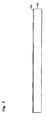
- a supporting board 101 of 200 micrometers thick, formed of a conducting material such as Cu is provided.
- a stop layer 121 is formed on the supporting board 101 by the electroplating method.
- the stop layer 121 is a nickel film 2 to 3 micrometers thick and is formed on the top surface of the supporting board 101 by using the supporting board 101 as an electrode by the electroplating method.
- the supporting board 101 works as an energizing path.
- the supporting board 101 is preferably a conductive material, or more preferably, a low-resistance material such as Cu.
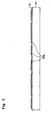
- pattern wiring 105b is formed on the supporting board 101 where a stop layer 121 is formed.
- the pattern wiring 105b forms a resist pattern (not shown) by way of photolithography.
- the resist pattern is used as a mask to deposit Cu by electroplating, and the resist pattern is removed to form the pattern wiring 105b.
- the insulating layer 106 is formed on the supporting board 101 so as to cover the pattern wiring 105b.
- the insulating layer 106 is made of a buildup material such as a thermosetting epoxy resin.
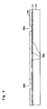
- a via hole 106A with laser beams so as to expose part of the pattern wiring 105b.
- desmear process is performed on the surface of the insulating layer 106 as required, and the residue in the via hole is removed and surface treatment made.
- a seed layer 107 of Cu is formed on the surface of the insulating layer 106 and the exposed pattern wiring 105b by electroless plating.
- the photolithography method is used to form a resist pattern (not shown).
- the resist pattern is used as a mask to apply electroplating with Cu to form a via plug 108a in the via hole 106A as well as form a pattern wiring 108b integrally connected to the via plug 108a on the insulating layer 106.
- the via plug 108a and the pattern wiring 108b constitute a wiring section 108.
- the resist pattern is stripped and an excessive seed layer 107 exposed is removed by etching.
- an insulating layer 106a is formed on the insulating layer 106 so as to cover the wiring section 108.
- the insulating layer 106a is a buildup material made of for example a thermosetting epoxy resin, the same material as that of the insulating layer 106.
- the insulating layer 106a and the insulating layer 106 are substantially integral.
- the insulating layer 106 is assumed to include the insulating layer 106a.
- an opening 106B is formed in the insulating layer 106 by using the laser beam machining method so as to expose part of the wiring section 108 (via plug 108a).
- the desmear process is applied to the insulating layer 106 as required to remove residue in the opening and perform surface treatment.
- the electroplating method is used to form a solder-connecting section 109 at the opening 106B.
- the semiconductor chip 110 has a stud bump 111 of Au formed thereon in advance.
- the stud bump 111 and the solder-connecting section 109 are positioned to correspond to each other and are flip-chip connected onto the wiring section 108 (pattern wiring 108b).
- an underfill layer 110A is formed between the semiconductor chip 110 and the insulating layer 106.
- the insulating layer 106b is formed on the insulating layer 106 so as to cover the semiconductor chip 110.
- the insulating layer 106b is a buildup material such as a thermosetting epoxy resin.
- the insulating layer 106b and the insulating layer 106 are substantially integral.
- the insulating layer 106 is assumed to include the insulating layer 106b.
- a via hole 106C is formed in the insulating layer 106.
- the via hole 106C is formed so as to expose the pattern wiring 108b for example by using the laser beam machining method.
- the desmear process is applied on the surface of the insulating layer 106 as required, thus removing residue in the via hole and performing surface treatment.
- a seed layer 112 made of Cu by the electroless plating method is formed on the surface of the insulating layer 106 and on the surface of the pattern wiring 108b.
- the seed layer 112 is electrically connected to a supporting board 101 made of Cu via the wiring section 108, pattern wiring 105b, and a stop layer 121 made of Ni.
- the photolithography method is used to form a resist pattern (not shown).
- the resist pattern is used as a mask to apply electroplating with Cu to form a via plug 113a in the via hole 106C as well as form a pattern wiring 113b connected to the via plug 113a on the insulating layer 106.
- the via plug 113a and the pattern wiring 113b constitute a wiring section 113.
- the resist pattern is stripped and an excessive seed layer exposed is removed by etching.
- an insulating layer (buildup layer) 106c made of for example a thermosetting epoxy resin is formed on the insulating layer 106 so as to cover the wiring section 108.
- the insulating layer 106c and the insulating layer 106 are substantially integral.
- the insulating layer 106 is assumed to include the insulating layer 106c.
- a process is made to laminate the insulating layer 106, pattern wiring 105b, and wiring sections 108, 113 on the supporting board 101.
- the insulating layer 106 is made of a resin material with a small elastic modulus and with a dense filler packed therein, which is unlikely to generate a warpage in the layer. Thus, No problematic warpage will take place in the processes show in Figs. 2 to 14.
- the supporting board 101 is removed by etching.
- the etching liquid used should dissolve the supporting board 101 (Cu) but not Ni of the stop layer 121. This causes the stop layer 121 to stop removal of the supporting board 101, thereby preventing the etching liquid from having an effect on the layers inside the stop layer 121, that is, the insulating layer 106, the pattern wiring 105b, and the wiring sections 108, 113. Management of removal processing in removing the supporting board 101 is made easy thus simplifying the manufacture of the wiring board 100.
- the stop layer 121 is removed with an etching liquid that dissolves Ni but does not resolve Cu.
- the supporting board 101 is removed, which means that no members support the insulating layer 106.
- the insulating layer 106 is about 200 to 300 micrometers thick assuring a rigidity to withstand handling.
- the absence of the supporting board 101 does not become an obstacle to processes shown in Fig. 16 and after that are described later.
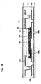
- a reinforcing layer 103 is formed under the insulating layer 106 and a reinforcing layer 114 is formed at the same time on the insulating layer 106.
- the insulating layer 106 is sandwiched by the reinforcing layers 103 and 114.
- the reinforcing layers 103 and 114 are formed simultaneously. This means that curing of the reinforcing layers 103 and 114 are performed simultaneously so that shrinkage of the reinforcing layers 103 and 114 on curing is uniformly applied from above and below the insulting layer 106, etc., thus preventing a possible warpage of the wiring board. Also, by performing the curing simultaneously, a heat history of the reinforcing layer 103 and a heat history of the reinforcing layer 114 can be identical.
- the reinforcing layers 103 and 114 are pressed and attached temporarily to the insulating layer 106, and then the curing is performed.
- the reinforcing layers 103 and 114 may be attached to the insulating layer 106 separately, or simultaneously.
- the reinforcing layers 103, 114 are formed for example by laminating a prepreg material under heat and pressure.
- the prepreg material has a structure where glass fibers are impregnated with an epoxy resin as mentioned earlier and has a higher post-heat-curing rigidity than a general buildup resin material.
- the elastic modulus (Young's modulus) of a buildup resin material is about 5GPa to 8GPa while the elastic modulus of a prepreg material is 20GPa or above, which shows the high rigidity of the latter that reduces a warpage in a wiring board.
- a via hole 103A is formed in the reinforcing layer 103 by using laser beams so as to expose pattern wiring 105b.
- via holes 114A are formed in the reinforcing layer 114 and an insulating layer 106 by using laser beams so as to expose a wiring section 113 (pattern wiring 113b).
- the via holes 103A and 114A are simultaneously formed.
- the desmear process is applied as required to the bottom surface of the reinforcing layer 103 and the top surface of the reinforcing layer 114 in order to remove residue in the via hole and surface treatment.
- seed layers 104, 115 of Cu are respectively formed on the bottom surface of the reinforcing layer 103 and the top surface of the reinforcing layer 114 (including part of the insulating layer 106 exposed from the via hole 114A) by the electroless plating method.
- the seed layers 104, 115 are simultaneously formed.
- the photolithography method is used to form a resist pattern (not shown) in the seed layer 104 and the seed layer 115.
- the resist pattern is used as a mask to apply electroplating with Cu to form a via plug 105a on the reinforcing layer 103 so as to provide connection to the pattern wiring 105b.
- the via plug 105a and the pattern wiring 105b constitute a wiring section 105.
- the resist pattern is used as a mask to form a via plug 116a by electroplating with Cu so as to provide connection to the pattern wiring 113b exposed from the via hole 114A formed in the reinforcing layer 114.
- pattern wiring 116b is formed on the reinforcing layer 114 to provide connection to the via plug 116a.
- the via plug 116a and the pattern wiring 116b constitute a wiring section 116.
- the resist pattern is stripped and the excessive seed layers 104, 115 exposed are removed by etching.
- a solder resist 119 is formed to cover the reinforcing layer 103 and an opening 119A is formed at a predetermined position where the wiring section 105 (via plug 105a) of the solder resist 119 is exposed.
- a solder resist 117 is formed so as to cover the reinforcing layer 114.
- An opening 117A is formed at a predetermined position where the wiring section 116 (pattern wiring 116b) of the solder resist 117 is exposed.
- the solder resist 117 including the opening 117A and the solder resist 119 including the opening 119A are simultaneously formed.
- an electrode 118 including for example an Au layer 118a and an Ni layer 118b is formed on the wiring section 116 (pattern wiring 116b) exposed from the opening 117A.
- An electrode 102 including for example an Au layer 102a and an Ni layer 102b is formed on the wiring section 105 (via plug 105a) exposed from the opening 119A (surface treatment). The electrode 102 and the electrode 118 are simultaneously formed.
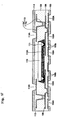
- solder ball 120 is formed on the electrode 102 to form the wiring board 100 shown in Fig. 1.
- the above manufacturing method is a buildup method that uses a coreless structure (structure without a supporting board).
- This approach provides a thin, compact and lightweight design of a wiring board.
- Use of the reinforcing layers 103, 114 reduces a warpage in the wiring board. This makes it possible to form a thin wiring board that includes a superfine wiring section.
- the wiring section 116 where the semiconductor chip 110 is embedded and wiring sections 105, 108, 113 are formed, and then the supporting board 101 is removed.
- the reinforcing layers 103 and 114 are simultaneously formed to sandwich the insulating layer 106 to which the supporting board 101 is not attached.
- each of the reinforcing layers 103, 114 show a large shrinkage on curing.
- the reinforcing layers 103, 114 are simultaneously formed so as to sandwich the insulating layer 106, the wiring section 116, etc.
- the shrinkage on curing is uniformly applied from above and below the insulating layer 106, the wiring section 116, etc., thus preventing a possible warpage.
- processing on the top surface of the insulating layer 106 and processing on the bottom surface shown in the figure take place simultaneously.
- layers are simultaneously formed on and under the insulating layer 106 thus facilitating the manufacturing process and reducing time required for manufacturing.
Landscapes
- Engineering & Computer Science (AREA)
- Manufacturing & Machinery (AREA)
- Microelectronics & Electronic Packaging (AREA)
- Production Of Multi-Layered Print Wiring Board (AREA)
Applications Claiming Priority (1)
| Application Number | Priority Date | Filing Date | Title |
|---|---|---|---|
| JP2005246438A JP2007059821A (ja) | 2005-08-26 | 2005-08-26 | 配線基板の製造方法 |
Publications (2)
| Publication Number | Publication Date |
|---|---|
| EP1758438A2 true EP1758438A2 (de) | 2007-02-28 |
| EP1758438A3 EP1758438A3 (de) | 2009-02-25 |
Family
ID=37607615
Family Applications (1)
| Application Number | Title | Priority Date | Filing Date |
|---|---|---|---|
| EP06017783A Withdrawn EP1758438A3 (de) | 2005-08-26 | 2006-08-25 | Herstellungsverfahren einer Leiterplatte |
Country Status (6)
| Country | Link |
|---|---|
| US (1) | US7937828B2 (de) |
| EP (1) | EP1758438A3 (de) |
| JP (1) | JP2007059821A (de) |
| KR (1) | KR20070024374A (de) |
| CN (1) | CN1921079B (de) |
| TW (1) | TW200717672A (de) |
Cited By (16)
| Publication number | Priority date | Publication date | Assignee | Title |
|---|---|---|---|---|
| EP2001047A1 (de) * | 2007-06-07 | 2008-12-10 | Semiconductor Energy Laboratory Co, Ltd. | Halbleiterbauelement |
| WO2008129424A3 (en) * | 2007-04-23 | 2008-12-18 | Cufer Asset Ltd Llc | Ultra-thin stacked chios packaging |
| EP2019425A1 (de) * | 2007-07-27 | 2009-01-28 | Semiconductor Energy Laboratory Co., Ltd. | Halbleiterbauelement und Verfahren zu seiner Herstellung |
| US7888163B2 (en) | 2008-06-06 | 2011-02-15 | Semiconductor Energy Laboratory Co., Ltd. | Semiconductor device and method for manufacturing the same |
| US8053253B2 (en) | 2008-06-06 | 2011-11-08 | Semiconductor Energy Laboratory Co., Ltd. | Method for manufacturing semiconductor device |
| US8133749B2 (en) | 2008-04-25 | 2012-03-13 | Semiconductor Energy Laboratory Co., Ltd. | Semiconductor device and method for manufacturing the same |
| US8148818B2 (en) | 2008-05-23 | 2012-04-03 | Semiconductor Energy Laboratory Co., Ltd. | Semiconductor device and method for manufacturing the same |
| US8169588B2 (en) | 2008-07-10 | 2012-05-01 | Semiconductor Energy Laboratory Co., Ltd. | Liquid crystal display device and method for manufacturing the same |
| EP2448378A1 (de) * | 2010-10-26 | 2012-05-02 | ATOTECH Deutschland GmbH | Verbundtoffbaumaterialien zum Einbetten aktiver Komponenten |
| US8237248B2 (en) | 2008-05-23 | 2012-08-07 | Semiconductor Energy Laboratory Co., Ltd. | Semiconductor device |
| US8264144B2 (en) | 2008-07-10 | 2012-09-11 | Semiconductor Energy Laboratory Co., Ltd. | Light emitting device and electronic device utilizing fibrous barrier layers impregnated with organic resin |
| US8284369B2 (en) | 2008-08-20 | 2012-10-09 | Semiconductor Energy Laboratory Co., Ltd. | Flexible light-emitting device, and method for fabricating the same |
| US8384209B2 (en) | 2008-05-12 | 2013-02-26 | Semiconductor Energy Laboratory Co., Ltd. | Semiconductor device and method for manufacturing semiconductor device |
| US8552498B2 (en) | 2008-09-19 | 2013-10-08 | Semiconductor Energy Laboratory Co., Ltd. | Semiconductor device and method for manufacturing the same |
| US8598719B2 (en) | 2008-06-12 | 2013-12-03 | Sumitomo Bakelite Company Limited | Semiconductor element mounting board |
| CN104183505A (zh) * | 2013-05-20 | 2014-12-03 | 矽品精密工业股份有限公司 | 半导体封装件的制法 |
Families Citing this family (44)
| Publication number | Priority date | Publication date | Assignee | Title |
|---|---|---|---|---|
| EP1970951A3 (de) * | 2007-03-13 | 2009-05-06 | Semiconductor Energy Laboratory Co., Ltd. | Halbleiterbauelement und Herstellungsverfahren dafür |
| TWI375999B (en) | 2007-06-07 | 2012-11-01 | Advanced Semiconductor Eng | Substrate with bumps process and structure |
| KR101354372B1 (ko) * | 2007-07-31 | 2014-01-23 | 삼성전자주식회사 | 인쇄회로기판 보강구조물 및 이를 이용한 집적회로 패키지 |
| WO2009031482A1 (en) * | 2007-09-07 | 2009-03-12 | Semiconductor Energy Laboratory Co., Ltd. | Semiconductor device and method for manufacturing the same |
| JP5096855B2 (ja) * | 2007-09-27 | 2012-12-12 | 新光電気工業株式会社 | 配線基板の製造方法及び配線基板 |
| CN101221908B (zh) * | 2008-01-29 | 2010-10-13 | 日月光半导体制造股份有限公司 | 具有凸块的基板工艺及其结构 |
| CN101515574B (zh) * | 2008-02-18 | 2011-06-22 | 旭德科技股份有限公司 | 芯片封装载板、芯片封装体及其制造方法 |
| KR100996914B1 (ko) * | 2008-06-19 | 2010-11-26 | 삼성전기주식회사 | 칩 내장 인쇄회로기판 및 그 제조방법 |
| TWI401000B (zh) * | 2008-07-23 | 2013-07-01 | 日本電氣股份有限公司 | 無核心層配線基板、半導體裝置及其製造方法 |
| WO2010032602A1 (en) | 2008-09-18 | 2010-03-25 | Semiconductor Energy Laboratory Co., Ltd. | Semiconductor device |
| WO2010038599A1 (en) * | 2008-10-01 | 2010-04-08 | Semiconductor Energy Laboratory Co., Ltd. | Semiconductor device |
| JP5147678B2 (ja) * | 2008-12-24 | 2013-02-20 | 新光電気工業株式会社 | 微細配線パッケージの製造方法 |
| JP5339928B2 (ja) * | 2009-01-15 | 2013-11-13 | 新光電気工業株式会社 | 配線基板及びその製造方法 |
| JPWO2010101167A1 (ja) * | 2009-03-05 | 2012-09-10 | 日本電気株式会社 | 半導体装置及びその製造方法 |
| KR20110039879A (ko) * | 2009-10-12 | 2011-04-20 | 삼성전기주식회사 | 전자부품 내장형 인쇄회로기판 및 그 제조방법 |
| WO2011089936A1 (ja) * | 2010-01-22 | 2011-07-28 | 日本電気株式会社 | 機能素子内蔵基板及び配線基板 |
| TWI420996B (zh) * | 2010-07-30 | 2013-12-21 | Lg伊諾特股份有限公司 | 印刷電路板及其製造方法 |
| KR101906408B1 (ko) * | 2011-10-04 | 2018-10-11 | 삼성전자주식회사 | 반도체 패키지 및 그 제조 방법 |
| JP2013211518A (ja) * | 2012-02-28 | 2013-10-10 | Ngk Spark Plug Co Ltd | 多層配線基板およびその製造方法 |
| CN103383927A (zh) * | 2012-05-03 | 2013-11-06 | 三星电子株式会社 | 半导体封装及其形成方法 |
| JP5981232B2 (ja) * | 2012-06-06 | 2016-08-31 | 新光電気工業株式会社 | 半導体パッケージ、半導体装置及び半導体パッケージの製造方法 |
| JP6092555B2 (ja) * | 2012-09-24 | 2017-03-08 | 新光電気工業株式会社 | 配線基板の製造方法 |
| JP6478309B2 (ja) * | 2012-12-31 | 2019-03-06 | サムソン エレクトロ−メカニックス カンパニーリミテッド. | 多層基板及び多層基板の製造方法 |
| JP6303443B2 (ja) * | 2013-11-27 | 2018-04-04 | Tdk株式会社 | Ic内蔵基板の製造方法 |
| KR102250997B1 (ko) | 2014-05-02 | 2021-05-12 | 삼성전자주식회사 | 반도체 패키지 |
| US20150366081A1 (en) * | 2014-06-15 | 2015-12-17 | Unimicron Technology Corp. | Manufacturing method for circuit structure embedded with electronic device |
| US9704735B2 (en) * | 2014-08-19 | 2017-07-11 | Intel Corporation | Dual side solder resist layers for coreless packages and packages with an embedded interconnect bridge and their methods of fabrication |
| JP6358431B2 (ja) | 2014-08-25 | 2018-07-18 | 新光電気工業株式会社 | 電子部品装置及びその製造方法 |
| TWI623251B (zh) * | 2014-08-29 | 2018-05-01 | 恆勁科技股份有限公司 | 中介基板之製法 |
| JP2016054188A (ja) * | 2014-09-03 | 2016-04-14 | 大日本印刷株式会社 | 部品内蔵配線基板、部品内蔵配線基板の製造方法、及び部品内蔵配線基板製造用の中間配線層 |
| TWI582861B (zh) * | 2014-09-12 | 2017-05-11 | 矽品精密工業股份有限公司 | 嵌埋元件之封裝結構及其製法 |
| US9941219B2 (en) | 2014-09-19 | 2018-04-10 | Intel Corporation | Control of warpage using ABF GC cavity for embedded die package |
| JP2017017238A (ja) * | 2015-07-03 | 2017-01-19 | 株式会社ジェイデバイス | 半導体装置及びその製造方法 |
| JP6451569B2 (ja) * | 2015-09-14 | 2019-01-16 | 株式会社デンソー | 電子装置 |
| KR102493463B1 (ko) * | 2016-01-18 | 2023-01-30 | 삼성전자 주식회사 | 인쇄회로기판, 이를 가지는 반도체 패키지, 및 인쇄회로기판의 제조 방법 |
| KR102466362B1 (ko) * | 2016-02-19 | 2022-11-15 | 삼성전자주식회사 | 지지 기판 및 이를 사용한 반도체 패키지의 제조방법 |
| US10276467B2 (en) * | 2016-03-25 | 2019-04-30 | Samsung Electro-Mechanics Co., Ltd. | Fan-out semiconductor package |
| KR101999625B1 (ko) * | 2016-03-25 | 2019-07-17 | 삼성전자주식회사 | 팬-아웃 반도체 패키지 |
| US9853011B2 (en) | 2016-03-29 | 2017-12-26 | Advanced Semiconductor Engineering, Inc. | Semiconductor package structure and method for manufacturing the same |
| US10763031B2 (en) * | 2016-08-30 | 2020-09-01 | Samsung Electro-Mechanics Co., Ltd. | Method of manufacturing an inductor |
| US11432402B2 (en) * | 2018-10-11 | 2022-08-30 | Microchip Technology Caldicot Limited | Flipped-conductor-patch lamination for ultra fine-line substrate creation |
| JP7211757B2 (ja) * | 2018-10-22 | 2023-01-24 | 新光電気工業株式会社 | 配線基板 |
| US10847400B2 (en) * | 2018-12-28 | 2020-11-24 | Applied Materials, Inc. | Adhesive-less substrate bonding to carrier plate |
| CN115274468A (zh) * | 2021-11-11 | 2022-11-01 | 天芯互联科技有限公司 | 芯片的封装方法以及封装机构 |
Citations (3)
| Publication number | Priority date | Publication date | Assignee | Title |
|---|---|---|---|---|
| US20040160752A1 (en) | 2003-02-18 | 2004-08-19 | Matsushita Electric Industrial Co. | Electronic component built-in module and method of manufacturing the same |
| US20050006142A1 (en) * | 2003-07-09 | 2005-01-13 | Matsushita Electric Industrial Co., Ltd. | Circuit board with in-built electronic component and method for manufacturing the same |
| WO2005004567A1 (ja) | 2003-07-04 | 2005-01-13 | Murata Manufacturing Co., Ltd. | 部品内蔵基板の製造方法 |
Family Cites Families (13)
| Publication number | Priority date | Publication date | Assignee | Title |
|---|---|---|---|---|
| JPH09139560A (ja) | 1995-11-14 | 1997-05-27 | Toshiba Corp | 回路基板装置およびその製造方法 |
| JP3635219B2 (ja) | 1999-03-11 | 2005-04-06 | 新光電気工業株式会社 | 半導体装置用多層基板及びその製造方法 |
| JP2002076637A (ja) | 2000-08-29 | 2002-03-15 | Matsushita Electric Ind Co Ltd | チップ部品内蔵基板及びその製造方法 |
| JP3760101B2 (ja) * | 2001-02-13 | 2006-03-29 | 富士通株式会社 | 多層プリント配線板およびその製造方法 |
| TW558743B (en) * | 2001-08-22 | 2003-10-21 | Semiconductor Energy Lab | Peeling method and method of manufacturing semiconductor device |
| KR100516795B1 (ko) * | 2001-10-31 | 2005-09-26 | 신꼬오덴기 고교 가부시키가이샤 | 반도체 장치용 다층 회로 기판의 제조 방법 |
| JP3492348B2 (ja) * | 2001-12-26 | 2004-02-03 | 新光電気工業株式会社 | 半導体装置用パッケージの製造方法 |
| TW200302685A (en) * | 2002-01-23 | 2003-08-01 | Matsushita Electric Industrial Co Ltd | Circuit component built-in module and method of manufacturing the same |
| JP2004079773A (ja) * | 2002-08-19 | 2004-03-11 | Taiyo Yuden Co Ltd | 多層プリント配線板及びその製造方法 |
| JP2004327624A (ja) | 2003-04-23 | 2004-11-18 | Shinko Electric Ind Co Ltd | 部品内蔵多層回路基板 |
| JP3904541B2 (ja) * | 2003-09-26 | 2007-04-11 | 沖電気工業株式会社 | 半導体装置内蔵基板の製造方法 |
| US6974724B2 (en) * | 2004-04-28 | 2005-12-13 | Nokia Corporation | Shielded laminated structure with embedded chips |
| US20060085058A1 (en) * | 2004-10-20 | 2006-04-20 | Rosenthal Arthur L | System and method for delivering a biologically active material to a body lumen |
-
2005
- 2005-08-26 JP JP2005246438A patent/JP2007059821A/ja active Pending
-
2006
- 2006-08-22 KR KR1020060079178A patent/KR20070024374A/ko not_active Withdrawn
- 2006-08-25 TW TW095131357A patent/TW200717672A/zh unknown
- 2006-08-25 CN CN2006101099819A patent/CN1921079B/zh active Active
- 2006-08-25 EP EP06017783A patent/EP1758438A3/de not_active Withdrawn
- 2006-08-25 US US11/509,684 patent/US7937828B2/en active Active
Patent Citations (3)
| Publication number | Priority date | Publication date | Assignee | Title |
|---|---|---|---|---|
| US20040160752A1 (en) | 2003-02-18 | 2004-08-19 | Matsushita Electric Industrial Co. | Electronic component built-in module and method of manufacturing the same |
| WO2005004567A1 (ja) | 2003-07-04 | 2005-01-13 | Murata Manufacturing Co., Ltd. | 部品内蔵基板の製造方法 |
| US20050006142A1 (en) * | 2003-07-09 | 2005-01-13 | Matsushita Electric Industrial Co., Ltd. | Circuit board with in-built electronic component and method for manufacturing the same |
Cited By (35)
| Publication number | Priority date | Publication date | Assignee | Title |
|---|---|---|---|---|
| WO2008129424A3 (en) * | 2007-04-23 | 2008-12-18 | Cufer Asset Ltd Llc | Ultra-thin stacked chios packaging |
| US7960210B2 (en) | 2007-04-23 | 2011-06-14 | Cufer Asset Ltd. L.L.C. | Ultra-thin chip packaging |
| CN101663747B (zh) * | 2007-04-23 | 2013-05-22 | 丘费尔资产股份有限公司 | 超薄堆叠的芯片封装 |
| EP2001047A1 (de) * | 2007-06-07 | 2008-12-10 | Semiconductor Energy Laboratory Co, Ltd. | Halbleiterbauelement |
| US7906847B2 (en) | 2007-06-07 | 2011-03-15 | Semiconductor Energy Laboratory Co., Ltd. | Semiconductor device |
| EP2019425A1 (de) * | 2007-07-27 | 2009-01-28 | Semiconductor Energy Laboratory Co., Ltd. | Halbleiterbauelement und Verfahren zu seiner Herstellung |
| US9412060B2 (en) | 2007-07-27 | 2016-08-09 | Semiconductor Energy Laboratory Co., Ltd. | Semiconductor device and method for manufacturing the same |
| US7932589B2 (en) | 2007-07-27 | 2011-04-26 | Semiconductor Energy Laboratory Co., Ltd. | Semiconductor device and method for manufacturing the same |
| US8872331B2 (en) | 2007-07-27 | 2014-10-28 | Semiconductor Energy Laboratory Co., Ltd. | Semiconductor device and method for manufacturing the same |
| US9171808B2 (en) | 2008-04-25 | 2015-10-27 | Semiconductor Energy Laboratory Co., Ltd. | Semiconductor device and method for manufacturing the same |
| US8133749B2 (en) | 2008-04-25 | 2012-03-13 | Semiconductor Energy Laboratory Co., Ltd. | Semiconductor device and method for manufacturing the same |
| US8637932B2 (en) | 2008-04-25 | 2014-01-28 | Semiconductor Energy Laboratory Co., Ltd. | Semiconductor device and method for manufacturing the same |
| US8384209B2 (en) | 2008-05-12 | 2013-02-26 | Semiconductor Energy Laboratory Co., Ltd. | Semiconductor device and method for manufacturing semiconductor device |
| US9048277B2 (en) | 2008-05-12 | 2015-06-02 | Semiconductor Energy Laboratory Co., Ltd. | Semiconductor device and method for manufacturing semiconductor device |
| US8148818B2 (en) | 2008-05-23 | 2012-04-03 | Semiconductor Energy Laboratory Co., Ltd. | Semiconductor device and method for manufacturing the same |
| US8237248B2 (en) | 2008-05-23 | 2012-08-07 | Semiconductor Energy Laboratory Co., Ltd. | Semiconductor device |
| US7888163B2 (en) | 2008-06-06 | 2011-02-15 | Semiconductor Energy Laboratory Co., Ltd. | Semiconductor device and method for manufacturing the same |
| US8420409B2 (en) | 2008-06-06 | 2013-04-16 | Semiconductor Energy Laboratory Co., Ltd. | Method for manufacturing semiconductor device |
| US8053253B2 (en) | 2008-06-06 | 2011-11-08 | Semiconductor Energy Laboratory Co., Ltd. | Method for manufacturing semiconductor device |
| US8598719B2 (en) | 2008-06-12 | 2013-12-03 | Sumitomo Bakelite Company Limited | Semiconductor element mounting board |
| US10079330B2 (en) | 2008-07-10 | 2018-09-18 | Semiconductor Energy Laboratory Co., Ltd. | Light emitting device and electronic device having an embedded pixel electrode |
| US11908976B2 (en) | 2008-07-10 | 2024-02-20 | Semiconductor Energy Laboratory Co., Ltd. | Light emitting device and electronic device |
| US11557697B2 (en) | 2008-07-10 | 2023-01-17 | Semiconductor Energy Laboratory Co., Ltd. | Flexible light emitting device comprising a polyimide resin |
| US8169588B2 (en) | 2008-07-10 | 2012-05-01 | Semiconductor Energy Laboratory Co., Ltd. | Liquid crystal display device and method for manufacturing the same |
| US8860306B2 (en) | 2008-07-10 | 2014-10-14 | Semiconductor Energy Laboratory Co., Ltd. | Display device having a fibrous encapsulating structure |
| US11101407B2 (en) | 2008-07-10 | 2021-08-24 | Semiconductor Energy Laboratory Co., Ltd. | Light emitting device sealed in a fibrous body to improve manufacturability and electronic device including the light emitting device |
| US10205062B2 (en) | 2008-07-10 | 2019-02-12 | Semiconductor Energy Laboratory Co., Ltd. | Light emitting device that is highly reliable, thin and is not damaged by external local pressure and electronic device |
| US8264144B2 (en) | 2008-07-10 | 2012-09-11 | Semiconductor Energy Laboratory Co., Ltd. | Light emitting device and electronic device utilizing fibrous barrier layers impregnated with organic resin |
| US8284369B2 (en) | 2008-08-20 | 2012-10-09 | Semiconductor Energy Laboratory Co., Ltd. | Flexible light-emitting device, and method for fabricating the same |
| US8957423B2 (en) | 2008-09-19 | 2015-02-17 | Semiconductor Energy Laboratory Co., Ltd. | Semiconductor device |
| US8552498B2 (en) | 2008-09-19 | 2013-10-08 | Semiconductor Energy Laboratory Co., Ltd. | Semiconductor device and method for manufacturing the same |
| WO2012055785A1 (en) * | 2010-10-26 | 2012-05-03 | Atotech Deutschland Gmbh | Composite build-up materials for embedding of active components |
| EP2448378A1 (de) * | 2010-10-26 | 2012-05-02 | ATOTECH Deutschland GmbH | Verbundtoffbaumaterialien zum Einbetten aktiver Komponenten |
| CN104183505B (zh) * | 2013-05-20 | 2017-04-05 | 矽品精密工业股份有限公司 | 半导体封装件的制法 |
| CN104183505A (zh) * | 2013-05-20 | 2014-12-03 | 矽品精密工业股份有限公司 | 半导体封装件的制法 |
Also Published As
| Publication number | Publication date |
|---|---|
| KR20070024374A (ko) | 2007-03-02 |
| JP2007059821A (ja) | 2007-03-08 |
| US7937828B2 (en) | 2011-05-10 |
| EP1758438A3 (de) | 2009-02-25 |
| US20070044303A1 (en) | 2007-03-01 |
| CN1921079A (zh) | 2007-02-28 |
| CN1921079B (zh) | 2010-07-28 |
| TW200717672A (en) | 2007-05-01 |
Similar Documents
| Publication | Publication Date | Title |
|---|---|---|
| US7937828B2 (en) | Method of manufacturing wiring board | |
| EP1740025B1 (de) | Leiterplatte und Verfahren zu deren Herstellung | |
| JP4874305B2 (ja) | 電気・電子部品内蔵回路基板とその製造方法 | |
| KR101988923B1 (ko) | 배선 기판 제조 방법, 배선 기판 제조용 지지체 및 배선 기판용 구조체 | |
| US20090135574A1 (en) | Wiring board, semiconductor device having wiring board, and method of manufacturing wiring board | |
| JP5367523B2 (ja) | 配線基板及び配線基板の製造方法 | |
| KR101281410B1 (ko) | 다층 배선기판 | |
| JPWO2010013366A1 (ja) | フレックスリジッド配線板及びその製造方法 | |
| US9334576B2 (en) | Wiring substrate and method of manufacturing wiring substrate | |
| JP2007096260A (ja) | 多層配線基板及びその製造方法 | |
| JP2010135721A (ja) | 金属バンプを持つプリント基板及びその製造方法 | |
| JP6880429B2 (ja) | 素子内蔵型印刷回路基板及びその製造方法 | |
| CN106340461B (zh) | 一种超薄无芯封装基板的加工方法和结构 | |
| KR101470706B1 (ko) | 다층 배선기판의 제조방법 | |
| US7772109B2 (en) | Manufacturing method of multilayer wiring substrate | |
| US10080292B2 (en) | Wiring board | |
| JP2004087701A (ja) | 多層配線構造の製造方法および半導体装置の搭載方法 | |
| JP2008270633A (ja) | 半導体素子内蔵基板 | |
| WO2014125567A1 (ja) | 部品内蔵基板及びその製造方法 | |
| US11605585B2 (en) | Flexible substrate and semiconductor apparatus | |
| JP2022015759A (ja) | 配線基板の製造方法 | |
| US20250081329A1 (en) | Wiring board and laminated wiring board | |
| KR101189330B1 (ko) | 인쇄회로기판 및 그의 제조 방법 | |
| JP2005244124A (ja) | 配線基板の製造方法 | |
| KR101340349B1 (ko) | 패키지 기판 및 이의 제조 방법 |
Legal Events
| Date | Code | Title | Description |
|---|---|---|---|
| PUAI | Public reference made under article 153(3) epc to a published international application that has entered the european phase |
Free format text: ORIGINAL CODE: 0009012 |
|
| AK | Designated contracting states |
Kind code of ref document: A2 Designated state(s): AT BE BG CH CY CZ DE DK EE ES FI FR GB GR HU IE IS IT LI LT LU LV MC NL PL PT RO SE SI SK TR |
|
| AX | Request for extension of the european patent |
Extension state: AL BA HR MK YU |
|
| PUAL | Search report despatched |
Free format text: ORIGINAL CODE: 0009013 |
|
| AK | Designated contracting states |
Kind code of ref document: A3 Designated state(s): AT BE BG CH CY CZ DE DK EE ES FI FR GB GR HU IE IS IT LI LT LU LV MC NL PL PT RO SE SI SK TR |
|
| AX | Request for extension of the european patent |
Extension state: AL BA HR MK RS |
|
| 17P | Request for examination filed |
Effective date: 20090811 |
|
| AKX | Designation fees paid |
Designated state(s): DE |
|
| 17Q | First examination report despatched |
Effective date: 20100406 |
|
| GRAP | Despatch of communication of intention to grant a patent |
Free format text: ORIGINAL CODE: EPIDOSNIGR1 |
|
| STAA | Information on the status of an ep patent application or granted ep patent |
Free format text: STATUS: THE APPLICATION IS DEEMED TO BE WITHDRAWN |
|
| 18D | Application deemed to be withdrawn |
Effective date: 20120218 |