EP1760037A1 - Verfahren zum Herstellen von mikromechanischen Strukturen - Google Patents
Verfahren zum Herstellen von mikromechanischen Strukturen Download PDFInfo
- Publication number
- EP1760037A1 EP1760037A1 EP05255430A EP05255430A EP1760037A1 EP 1760037 A1 EP1760037 A1 EP 1760037A1 EP 05255430 A EP05255430 A EP 05255430A EP 05255430 A EP05255430 A EP 05255430A EP 1760037 A1 EP1760037 A1 EP 1760037A1
- Authority
- EP
- European Patent Office
- Prior art keywords
- micromechanical structure
- manufacturing
- substrate
- surface layer
- etching
- Prior art date
- Legal status (The legal status is an assumption and is not a legal conclusion. Google has not performed a legal analysis and makes no representation as to the accuracy of the status listed.)
- Withdrawn
Links
- 238000000034 method Methods 0.000 title claims abstract description 41
- 238000004519 manufacturing process Methods 0.000 title claims abstract description 31
- 239000000758 substrate Substances 0.000 claims abstract description 34
- 238000005530 etching Methods 0.000 claims abstract description 20
- XUIMIQQOPSSXEZ-UHFFFAOYSA-N Silicon Chemical compound [Si] XUIMIQQOPSSXEZ-UHFFFAOYSA-N 0.000 claims abstract description 19
- 229910052710 silicon Inorganic materials 0.000 claims abstract description 19
- 239000010703 silicon Substances 0.000 claims abstract description 19
- 239000002344 surface layer Substances 0.000 claims abstract description 16
- 239000010410 layer Substances 0.000 claims description 9
- 239000000463 material Substances 0.000 claims description 9
- 229910021420 polycrystalline silicon Inorganic materials 0.000 claims description 7
- 238000001312 dry etching Methods 0.000 claims description 4
- 229910021421 monocrystalline silicon Inorganic materials 0.000 claims description 4
- 238000000151 deposition Methods 0.000 claims description 3
- 238000005468 ion implantation Methods 0.000 claims description 3
- 229910010380 TiNi Inorganic materials 0.000 claims description 2
- 230000008021 deposition Effects 0.000 claims description 2
- 238000009792 diffusion process Methods 0.000 claims description 2
- 229910052759 nickel Inorganic materials 0.000 claims description 2
- 230000003647 oxidation Effects 0.000 claims description 2
- 238000007254 oxidation reaction Methods 0.000 claims description 2
- 229920005591 polysilicon Polymers 0.000 claims description 2
- 229910010271 silicon carbide Inorganic materials 0.000 claims description 2
- 229910052719 titanium Inorganic materials 0.000 claims description 2
- 230000000063 preceeding effect Effects 0.000 claims 2
- 229910003465 moissanite Inorganic materials 0.000 claims 1
- VYPSYNLAJGMNEJ-UHFFFAOYSA-N Silicium dioxide Chemical compound O=[Si]=O VYPSYNLAJGMNEJ-UHFFFAOYSA-N 0.000 description 6
- 239000010409 thin film Substances 0.000 description 5
- 238000005459 micromachining Methods 0.000 description 4
- 238000001020 plasma etching Methods 0.000 description 3
- 235000012239 silicon dioxide Nutrition 0.000 description 3
- 239000000377 silicon dioxide Substances 0.000 description 3
- 230000015572 biosynthetic process Effects 0.000 description 2
- 239000010408 film Substances 0.000 description 2
- 229910052581 Si3N4 Inorganic materials 0.000 description 1
- HMDDXIMCDZRSNE-UHFFFAOYSA-N [C].[Si] Chemical compound [C].[Si] HMDDXIMCDZRSNE-UHFFFAOYSA-N 0.000 description 1
- LEVVHYCKPQWKOP-UHFFFAOYSA-N [Si].[Ge] Chemical compound [Si].[Ge] LEVVHYCKPQWKOP-UHFFFAOYSA-N 0.000 description 1
- 229910045601 alloy Inorganic materials 0.000 description 1
- 239000000956 alloy Substances 0.000 description 1
- 238000000347 anisotropic wet etching Methods 0.000 description 1
- 229910052799 carbon Inorganic materials 0.000 description 1
- 239000003989 dielectric material Substances 0.000 description 1
- 239000002184 metal Substances 0.000 description 1
- 229910052751 metal Inorganic materials 0.000 description 1
- 229910052750 molybdenum Inorganic materials 0.000 description 1
- 238000004806 packaging method and process Methods 0.000 description 1
- 239000004065 semiconductor Substances 0.000 description 1
- 229910001285 shape-memory alloy Inorganic materials 0.000 description 1
- HBMJWWWQQXIZIP-UHFFFAOYSA-N silicon carbide Chemical compound [Si+]#[C-] HBMJWWWQQXIZIP-UHFFFAOYSA-N 0.000 description 1
- HQVNEWCFYHHQES-UHFFFAOYSA-N silicon nitride Chemical compound N12[Si]34N5[Si]62N3[Si]51N64 HQVNEWCFYHHQES-UHFFFAOYSA-N 0.000 description 1
- 229910052721 tungsten Inorganic materials 0.000 description 1
Images

Classifications
-
- B—PERFORMING OPERATIONS; TRANSPORTING
- B81—MICROSTRUCTURAL TECHNOLOGY
- B81C—PROCESSES OR APPARATUS SPECIALLY ADAPTED FOR THE MANUFACTURE OR TREATMENT OF MICROSTRUCTURAL DEVICES OR SYSTEMS
- B81C1/00—Manufacture or treatment of devices or systems in or on a substrate
- B81C1/00015—Manufacture or treatment of devices or systems in or on a substrate for manufacturing microsystems
- B81C1/00023—Manufacture or treatment of devices or systems in or on a substrate for manufacturing microsystems without movable or flexible elements
- B81C1/00103—Structures having a predefined profile, e.g. sloped or rounded grooves
-
- B—PERFORMING OPERATIONS; TRANSPORTING
- B81—MICROSTRUCTURAL TECHNOLOGY
- B81C—PROCESSES OR APPARATUS SPECIALLY ADAPTED FOR THE MANUFACTURE OR TREATMENT OF MICROSTRUCTURAL DEVICES OR SYSTEMS
- B81C99/00—Subject matter not provided for in other groups of this subclass
- B81C99/0075—Manufacture of substrate-free structures
- B81C99/008—Manufacture of substrate-free structures separating the processed structure from a mother substrate
-
- B—PERFORMING OPERATIONS; TRANSPORTING
- B81—MICROSTRUCTURAL TECHNOLOGY
- B81B—MICROSTRUCTURAL DEVICES OR SYSTEMS, e.g. MICROMECHANICAL DEVICES
- B81B2203/00—Basic microelectromechanical structures
- B81B2203/03—Static structures
- B81B2203/0369—Static structures characterized by their profile
- B81B2203/0384—Static structures characterized by their profile sloped profile
Definitions
- the present invention relates to the manufacture of micromechanical structures for use in micro electromechanical devices such as inertial devices.
- the invention relates to a method of manufacturing microstructures such as thin asymmetric springs, using bulk etching and bulk and/or surface micromachining techniques.
- Micro electromechanical systems are becoming increasingly important in the manufacture of inertial devices such as angular rate sensors and multiple axis accelerometers.
- Micromechanical structures such as asymmetric springs, diaphragms and mass-spring systems are increasingly used in such devices, where these structures are used to obtain in-plane movements of structures when applying out-of-plane forces.
- the manufacturing methods of these structures generally involve bulk micromachining techniques.
- Known devices which employ such methods include devices for measuring force components using monocrystalline materials, and 3-axis accelerometers. Devices for measuring angular velocity and angular rate sensors are also known to employ such micromechanical structures.
- the present invention seeks to overcome the aforementioned problems, by providing an alternative manufacturing method which can be used to build micromechanical structures such as thin asymmetric springs with a thickness in the sub-micron to 20 micron range and a width in the range of 1 micron or more, in an efficient and effective manufacturing method.
- a method for manufacturing a micromechanical structure comprising the steps of; providing a silicon substrate; etching the silicon substrate to define a section upon which the micromechanical structure can be formed; forming a surface layer on the surface of the substrate; etching to form a micromechanical structure from the surface layer; and etching to release the micromechanical structure from the substrate.
- Implementation of the present invention leads to the manufacture of much thinner asymmetric springs and related micromechanical structures, thereby providing greater flexibility in the manufacture of inertial devices in which in-plane movements of micromechanical structures occur when applying out-of-plane forces to the structures.
- This method may also be employed when manufacturing parts for different types of actuators, for example parts for microvalves, micropumps, microgrippers, microhandling, microbiotics, etc.
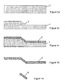
- the first step for manufacturing asymmetric springs in single crystal silicon is to provide a silicon substrate 1 on which the springs can be formed.
- the us of p-type silicon in the (100) plane is described, however other substrates such as (110) silicon can be used.
- an anisotropic etching technique is used to etch the section of the silicon substrate 1 in the (111) plane, defining a wall 2 along this plane as illustrated in figure 1 b.
- Figure 1c illustrates the formation of a doped surface layer 3 on the substrate 1.
- the n-type surface layer 3 is built by ion implantation and diffusion, and lies across the (111) wall 2 etched on the silicon substrate 1.
- the surface layer 3 is then detached from the substrate 1 (figure 1d) using an etch-stop against pn-junction technique in order to form the asymmetric feature and thickness of an asymmetric spring 4.
- asymmetric spring 4 it is necessary to release the asymmetric spring 4 from the remainder of the surface layer 3. This is done by standard photolithographic methods and dry-etching such as reactive ion etching (RIE), in order to create the length of the spring 4, which is shaped by the (111) silicon substrate wall 2.
- RIE reactive ion etching
- This example of the present invention uses a combination of anisotropic wet etching, doping by ion implantation, etch-stop against pn-junction and dry etching techniques to create thin asymmetric springs in single-crystal silicon.
- the bulk micromachining techniques described can then be combined with other processes to build complete sensor chips and other micromechanical devices, for example, methods for wafer level packaging, as described in European patent publication no. 1460037 , can be employed in order to manufacture complete multiple axis inertial sensor chips packed on wafer level.
- FIG. 2 A further example of the manufacturing method of the present invention is illustrated in figure 2.
- This sequence of steps can be used to create out-of-plane asymmetric springs in poly-silicon or other deposited thin-film materials.
- a p-type silicon substrate 5 in the (100) plane is provided on which to base the formation of the asymmetric springs.
- Anisotropic etching is performed to define a wall 6 along the (111) plane of the substrate 5 (figure 2b).
- a sacrificial layer 7 is created above the etched silicon substrate 5, as shown in figure 2c.
- the sacrificial layer 7 can be formed by thermal oxidation, or by depositing, for example, silicon dioxide onto the substrate 5.
- the sacrificial layer 7 can be composed of thermally grown silicon dioxide, deposited doped or undoped silicon dioxide, or other thin-film material that can be selectively removed and that can withstand the deposition temperature of the surface layer.
- a layer of, for example, poly-silicon 8, from which an asymmetric spring 9 will eventually be formed, is then deposited on the sacrificial layer 7 (figure 2c).
- the poly-silicon layer 8 and sacrificial layer 7 are etched to form the asymmetric spring 9 and to release the micromechanical structure from the substrate 5, as shown in figure 2d.
- the above steps therefore use a combination of bulk etching and surface-micromachining to create micromechanical structures such as thin asymmetric springs.
- This example of the present invention can be extended to build two-axis angular rate sensors and three-axis accelerometers as full single-chip structures.
- out-of-plane springs can also be manufactured by etchings at different angles to the substrate surface plane. For example, different angles can be created on the substrate by using isotropic etching and deep, near 90° vertical etching.
- Micro mechanical structures such as thin springs and mass-spring systems for inertial devices can be made with a large variety of geometries using the method of the present invention.
- wet isotropic etching can be used, resulting in curved elements, or dry RIE etching can be used.
- Alternative thin-film materials to poly-silicon may be used in the present invention, including strong elastic dielectrics such as silicon-nitride, other semiconductor materials such as poly silicon germanium or silicon carbon, silicon-carbide, diamond-like-carbon and different metal films or insulating films which perform well as spring material, elastic thin-film materials such as Mo, W, Ti and Ni, and alloys including the shape-memory alloy TiNi.
- strong elastic dielectrics such as silicon-nitride, other semiconductor materials such as poly silicon germanium or silicon carbon, silicon-carbide, diamond-like-carbon and different metal films or insulating films which perform well as spring material
- elastic thin-film materials such as Mo, W, Ti and Ni, and alloys including the shape-memory alloy TiNi.
- the present invention therefore provides an efficient method of producing micromechanical structures such as thin asymmetric springs, which are a great deal thinner than those obtained by previous known methods. This allows for smaller, more compact and less expensive mircromechanical devices to be built with plates and asymmetric springs as required to obtain in-plane movements when applying out-of-plane forces, such as angular rate sensors and multiple axis accelerometers.
Landscapes
- Engineering & Computer Science (AREA)
- Manufacturing & Machinery (AREA)
- Microelectronics & Electronic Packaging (AREA)
- Chemical & Material Sciences (AREA)
- Analytical Chemistry (AREA)
- Micromachines (AREA)
- Gyroscopes (AREA)
- Pressure Sensors (AREA)
Priority Applications (4)
| Application Number | Priority Date | Filing Date | Title |
|---|---|---|---|
| EP05255430A EP1760037A1 (de) | 2005-09-06 | 2005-09-06 | Verfahren zum Herstellen von mikromechanischen Strukturen |
| EP20060119036 EP1760038B1 (de) | 2005-09-06 | 2006-08-16 | Verfahren zum Herstellen eines Masse-Feder Systems |
| US11/515,914 US20070062280A1 (en) | 2005-09-06 | 2006-09-06 | Method for manufacturing a mass-spring system |
| JP2006241839A JP2007069343A (ja) | 2005-09-06 | 2006-09-06 | マススプリング系の製造方法、マススプリング系、加速度系および慣性計測装置 |
Applications Claiming Priority (1)
| Application Number | Priority Date | Filing Date | Title |
|---|---|---|---|
| EP05255430A EP1760037A1 (de) | 2005-09-06 | 2005-09-06 | Verfahren zum Herstellen von mikromechanischen Strukturen |
Publications (1)
| Publication Number | Publication Date |
|---|---|
| EP1760037A1 true EP1760037A1 (de) | 2007-03-07 |
Family
ID=35064775
Family Applications (1)
| Application Number | Title | Priority Date | Filing Date |
|---|---|---|---|
| EP05255430A Withdrawn EP1760037A1 (de) | 2005-09-06 | 2005-09-06 | Verfahren zum Herstellen von mikromechanischen Strukturen |
Country Status (3)
| Country | Link |
|---|---|
| US (1) | US20070062280A1 (de) |
| EP (1) | EP1760037A1 (de) |
| JP (1) | JP2007069343A (de) |
Families Citing this family (4)
| Publication number | Priority date | Publication date | Assignee | Title |
|---|---|---|---|---|
| FR2857002B1 (fr) * | 2003-07-04 | 2005-10-21 | Commissariat Energie Atomique | Procede de desolidarisation d'une couche utile et composant obtenu par ce procede |
| JP4983483B2 (ja) * | 2007-08-30 | 2012-07-25 | ヤマハ株式会社 | 精密部品の製造方法 |
| DE102007051591B4 (de) * | 2007-10-12 | 2019-04-25 | Robert Bosch Gmbh | Mikromechanische Vorrichtung mit Antriebsrahmen |
| JP5357166B2 (ja) * | 2008-09-22 | 2013-12-04 | アルプス電気株式会社 | Memsセンサ及び検出装置 |
Citations (7)
| Publication number | Priority date | Publication date | Assignee | Title |
|---|---|---|---|---|
| US4342227A (en) * | 1980-12-24 | 1982-08-03 | International Business Machines Corporation | Planar semiconductor three direction acceleration detecting device and method of fabrication |
| EP0343784A2 (de) * | 1988-05-27 | 1989-11-29 | Ford Motor Company Limited | Herstellungsverfahren eines Silizium-Kraftwandlers |
| US5242533A (en) * | 1991-03-05 | 1993-09-07 | Robert Bosch Gmbh | Method of structuring a semiconductor chip |
| US20020020053A1 (en) * | 1999-12-20 | 2002-02-21 | Fonash Stephen J. | Deposited thin films and their use in separation and sacrificial layer applications |
| US20020135033A1 (en) * | 2001-03-08 | 2002-09-26 | Masaki Hara | Micro-mirror and a method for fabricating the same |
| EP1460037A1 (de) | 2003-03-18 | 2004-09-22 | SensoNor asa | Mehrlagiges Bauelement und dessen Herstellungsverfahren |
| WO2004083111A1 (en) * | 2003-03-21 | 2004-09-30 | Technische Universiteit Delft | A method for manfacturing a membrane in a (111) surface of a (100) silicium wafer |
Family Cites Families (1)
| Publication number | Priority date | Publication date | Assignee | Title |
|---|---|---|---|---|
| US7091057B2 (en) * | 2003-12-19 | 2006-08-15 | Agency For Science, Technology And Research | Method of making a single-crystal-silicon 3D micromirror |
-
2005
- 2005-09-06 EP EP05255430A patent/EP1760037A1/de not_active Withdrawn
-
2006
- 2006-09-06 US US11/515,914 patent/US20070062280A1/en not_active Abandoned
- 2006-09-06 JP JP2006241839A patent/JP2007069343A/ja not_active Withdrawn
Patent Citations (7)
| Publication number | Priority date | Publication date | Assignee | Title |
|---|---|---|---|---|
| US4342227A (en) * | 1980-12-24 | 1982-08-03 | International Business Machines Corporation | Planar semiconductor three direction acceleration detecting device and method of fabrication |
| EP0343784A2 (de) * | 1988-05-27 | 1989-11-29 | Ford Motor Company Limited | Herstellungsverfahren eines Silizium-Kraftwandlers |
| US5242533A (en) * | 1991-03-05 | 1993-09-07 | Robert Bosch Gmbh | Method of structuring a semiconductor chip |
| US20020020053A1 (en) * | 1999-12-20 | 2002-02-21 | Fonash Stephen J. | Deposited thin films and their use in separation and sacrificial layer applications |
| US20020135033A1 (en) * | 2001-03-08 | 2002-09-26 | Masaki Hara | Micro-mirror and a method for fabricating the same |
| EP1460037A1 (de) | 2003-03-18 | 2004-09-22 | SensoNor asa | Mehrlagiges Bauelement und dessen Herstellungsverfahren |
| WO2004083111A1 (en) * | 2003-03-21 | 2004-09-30 | Technische Universiteit Delft | A method for manfacturing a membrane in a (111) surface of a (100) silicium wafer |
Also Published As
| Publication number | Publication date |
|---|---|
| JP2007069343A (ja) | 2007-03-22 |
| US20070062280A1 (en) | 2007-03-22 |
Similar Documents
| Publication | Publication Date | Title |
|---|---|---|
| US6787052B1 (en) | Method for fabricating microstructures with deep anisotropic etching of thick silicon wafers | |
| US7122395B2 (en) | Method of forming semiconductor devices through epitaxy | |
| CN103373700B (zh) | 用于在半导体基底内部形成空腔的方法 | |
| Oosterbroek et al. | Etching methodologies in< 111>-oriented silicon wafers | |
| US20150192487A1 (en) | Low pressure sensors and flow sensors | |
| CN106145024A (zh) | 运动微机电系统(mems)封装件 | |
| US20080050845A1 (en) | Microelectromechanical systems encapsulation process | |
| JP2012506616A (ja) | ウェーハレベルでパッケージングされたmemsデバイス | |
| Pal et al. | Complex three-dimensional structures in Si {1 0 0} using wet bulk micromachining | |
| EP3095754B1 (de) | Niederdrucksensor und flusssensor | |
| Kim et al. | A high-aspect-ratio comb actuator using UV-LIGA surface micromachining and (110) silicon bulk micromachining | |
| EP1760037A1 (de) | Verfahren zum Herstellen von mikromechanischen Strukturen | |
| Lee et al. | Surface/bulk micromachining (SBM) process and deep trench oxide isolation method for MEMS | |
| EP1760038B1 (de) | Verfahren zum Herstellen eines Masse-Feder Systems | |
| CN111017862B (zh) | Mems桥梁柱结构及形成方法 | |
| EP4232406B1 (de) | Verfahren zur herstellung einer mems-vorrichtung | |
| Zorman et al. | Materials for microelectromechanical systems | |
| HUP0600488A2 (en) | Method for producing micromechanical elements can be integrated into cmos technology, carrying monolith si and monolith sio produced by porous si micromanufacturing process | |
| Tsai et al. | Surface micromachined turbines | |
| CN110002395B (zh) | 一种压阻式双轴运动传感器及其制作方法 | |
| Allen | 3 MEMS Fabrication | |
| Zhao et al. | Sacrificial grid release technology: a versatile release concept for MEMS structures | |
| French | Integration of silicon MEMS devices: Materials and processing considerations | |
| Rao et al. | Microstructures with protected convex corners in modified KOH solution exhibiting high-speed silicon etching | |
| Zorman et al. | Material aspects of micro-and nanoelectromechanical systems |
Legal Events
| Date | Code | Title | Description |
|---|---|---|---|
| PUAI | Public reference made under article 153(3) epc to a published international application that has entered the european phase |
Free format text: ORIGINAL CODE: 0009012 |
|
| AK | Designated contracting states |
Kind code of ref document: A1 Designated state(s): AT BE BG CH CY CZ DE DK EE ES FI FR GB GR HU IE IS IT LI LT LU LV MC NL PL PT RO SE SI SK TR |
|
| AX | Request for extension of the european patent |
Extension state: AL BA HR MK YU |
|
| AKX | Designation fees paid | ||
| REG | Reference to a national code |
Ref country code: DE Ref legal event code: 8566 |
|
| STAA | Information on the status of an ep patent application or granted ep patent |
Free format text: STATUS: THE APPLICATION IS DEEMED TO BE WITHDRAWN |
|
| 18D | Application deemed to be withdrawn |
Effective date: 20070908 |