EP1760801A2 - Films prismatiques microstructurés utilisés pour l'insertion d'images des OLEDs - Google Patents
Films prismatiques microstructurés utilisés pour l'insertion d'images des OLEDs Download PDFInfo
- Publication number
- EP1760801A2 EP1760801A2 EP06018045A EP06018045A EP1760801A2 EP 1760801 A2 EP1760801 A2 EP 1760801A2 EP 06018045 A EP06018045 A EP 06018045A EP 06018045 A EP06018045 A EP 06018045A EP 1760801 A2 EP1760801 A2 EP 1760801A2
- Authority
- EP
- European Patent Office
- Prior art keywords
- oled device
- light
- oled
- film
- features
- Prior art date
- Legal status (The legal status is an assumption and is not a legal conclusion. Google has not performed a legal analysis and makes no representation as to the accuracy of the status listed.)
- Withdrawn
Links
- 238000002156 mixing Methods 0.000 title description 6
- 239000000758 substrate Substances 0.000 claims abstract description 32
- 239000000203 mixture Substances 0.000 claims description 4
- 230000000737 periodic effect Effects 0.000 claims description 2
- 239000010408 film Substances 0.000 description 48
- 239000010410 layer Substances 0.000 description 29
- 239000000463 material Substances 0.000 description 17
- 239000012044 organic layer Substances 0.000 description 7
- 239000011521 glass Substances 0.000 description 6
- 239000004065 semiconductor Substances 0.000 description 6
- 239000003086 colorant Substances 0.000 description 5
- 238000000151 deposition Methods 0.000 description 5
- 229920000123 polythiophene Polymers 0.000 description 5
- 230000000694 effects Effects 0.000 description 4
- 238000005259 measurement Methods 0.000 description 4
- 229920000642 polymer Polymers 0.000 description 4
- 150000003384 small molecules Chemical class 0.000 description 4
- 239000002019 doping agent Substances 0.000 description 3
- 238000002347 injection Methods 0.000 description 3
- 239000007924 injection Substances 0.000 description 3
- 238000000034 method Methods 0.000 description 3
- 239000004033 plastic Substances 0.000 description 3
- 229920003023 plastic Polymers 0.000 description 3
- 229920000767 polyaniline Polymers 0.000 description 3
- 229920000144 PEDOT:PSS Polymers 0.000 description 2
- KDLHZDBZIXYQEI-UHFFFAOYSA-N Palladium Chemical compound [Pd] KDLHZDBZIXYQEI-UHFFFAOYSA-N 0.000 description 2
- 229920001609 Poly(3,4-ethylenedioxythiophene) Polymers 0.000 description 2
- 238000010168 coupling process Methods 0.000 description 2
- 238000005859 coupling reaction Methods 0.000 description 2
- 238000003618 dip coating Methods 0.000 description 2
- 230000006872 improvement Effects 0.000 description 2
- AMGQUBHHOARCQH-UHFFFAOYSA-N indium;oxotin Chemical compound [In].[Sn]=O AMGQUBHHOARCQH-UHFFFAOYSA-N 0.000 description 2
- 238000007641 inkjet printing Methods 0.000 description 2
- 238000004519 manufacturing process Methods 0.000 description 2
- 229910052751 metal Inorganic materials 0.000 description 2
- 239000002184 metal Substances 0.000 description 2
- 239000011368 organic material Substances 0.000 description 2
- 125000002524 organometallic group Chemical group 0.000 description 2
- BASFCYQUMIYNBI-UHFFFAOYSA-N platinum Chemical compound [Pt] BASFCYQUMIYNBI-UHFFFAOYSA-N 0.000 description 2
- -1 poly(3,4-ethylenedioxythiophene) Polymers 0.000 description 2
- 239000000243 solution Substances 0.000 description 2
- 238000001228 spectrum Methods 0.000 description 2
- 238000004528 spin coating Methods 0.000 description 2
- 238000004544 sputter deposition Methods 0.000 description 2
- 229920001621 AMOLED Polymers 0.000 description 1
- 239000004925 Acrylic resin Substances 0.000 description 1
- 229920000178 Acrylic resin Polymers 0.000 description 1
- OKTJSMMVPCPJKN-UHFFFAOYSA-N Carbon Chemical compound [C] OKTJSMMVPCPJKN-UHFFFAOYSA-N 0.000 description 1
- NIXOWILDQLNWCW-UHFFFAOYSA-N acrylic acid group Chemical group C(C=C)(=O)O NIXOWILDQLNWCW-UHFFFAOYSA-N 0.000 description 1
- 239000000853 adhesive Substances 0.000 description 1
- 230000001070 adhesive effect Effects 0.000 description 1
- 239000010405 anode material Substances 0.000 description 1
- 238000003491 array Methods 0.000 description 1
- 230000004888 barrier function Effects 0.000 description 1
- 230000000903 blocking effect Effects 0.000 description 1
- 125000000609 carbazolyl group Chemical class C1(=CC=CC=2C3=CC=CC=C3NC12)* 0.000 description 1
- 239000002800 charge carrier Substances 0.000 description 1
- 238000005229 chemical vapour deposition Methods 0.000 description 1
- 239000011248 coating agent Substances 0.000 description 1
- 238000000576 coating method Methods 0.000 description 1
- 239000002322 conducting polymer Substances 0.000 description 1
- 229920001940 conductive polymer Polymers 0.000 description 1
- 238000010276 construction Methods 0.000 description 1
- 229920001577 copolymer Polymers 0.000 description 1
- XCJYREBRNVKWGJ-UHFFFAOYSA-N copper(II) phthalocyanine Chemical compound [Cu+2].C12=CC=CC=C2C(N=C2[N-]C(C3=CC=CC=C32)=N2)=NC1=NC([C]1C=CC=CC1=1)=NC=1N=C1[C]3C=CC=CC3=C2[N-]1 XCJYREBRNVKWGJ-UHFFFAOYSA-N 0.000 description 1
- 230000008021 deposition Effects 0.000 description 1
- 238000009792 diffusion process Methods 0.000 description 1
- 238000009826 distribution Methods 0.000 description 1
- 230000005684 electric field Effects 0.000 description 1
- 238000000313 electron-beam-induced deposition Methods 0.000 description 1
- 238000000295 emission spectrum Methods 0.000 description 1
- 238000005516 engineering process Methods 0.000 description 1
- 230000002708 enhancing effect Effects 0.000 description 1
- 238000000605 extraction Methods 0.000 description 1
- 239000011888 foil Substances 0.000 description 1
- 239000003292 glue Substances 0.000 description 1
- PCHJSUWPFVWCPO-UHFFFAOYSA-N gold Chemical compound [Au] PCHJSUWPFVWCPO-UHFFFAOYSA-N 0.000 description 1
- 229910052737 gold Inorganic materials 0.000 description 1
- 239000010931 gold Substances 0.000 description 1
- 229910002804 graphite Inorganic materials 0.000 description 1
- 239000010439 graphite Substances 0.000 description 1
- RBTKNAXYKSUFRK-UHFFFAOYSA-N heliogen blue Chemical compound [Cu].[N-]1C2=C(C=CC=C3)C3=C1N=C([N-]1)C3=CC=CC=C3C1=NC([N-]1)=C(C=CC=C3)C3=C1N=C([N-]1)C3=CC=CC=C3C1=N2 RBTKNAXYKSUFRK-UHFFFAOYSA-N 0.000 description 1
- 229910052738 indium Inorganic materials 0.000 description 1
- APFVFJFRJDLVQX-UHFFFAOYSA-N indium atom Chemical compound [In] APFVFJFRJDLVQX-UHFFFAOYSA-N 0.000 description 1
- 229910010272 inorganic material Inorganic materials 0.000 description 1
- 239000011147 inorganic material Substances 0.000 description 1
- 229910000464 lead oxide Inorganic materials 0.000 description 1
- 239000011159 matrix material Substances 0.000 description 1
- 239000007769 metal material Substances 0.000 description 1
- 150000002739 metals Chemical class 0.000 description 1
- 238000012986 modification Methods 0.000 description 1
- 230000004048 modification Effects 0.000 description 1
- DCZNSJVFOQPSRV-UHFFFAOYSA-N n,n-diphenyl-4-[4-(n-phenylanilino)phenyl]aniline Chemical compound C1=CC=CC=C1N(C=1C=CC(=CC=1)C=1C=CC(=CC=1)N(C=1C=CC=CC=1)C=1C=CC=CC=1)C1=CC=CC=C1 DCZNSJVFOQPSRV-UHFFFAOYSA-N 0.000 description 1
- YEXPOXQUZXUXJW-UHFFFAOYSA-N oxolead Chemical compound [Pb]=O YEXPOXQUZXUXJW-UHFFFAOYSA-N 0.000 description 1
- 229910052763 palladium Inorganic materials 0.000 description 1
- SLIUAWYAILUBJU-UHFFFAOYSA-N pentacene Chemical compound C1=CC=CC2=CC3=CC4=CC5=CC=CC=C5C=C4C=C3C=C21 SLIUAWYAILUBJU-UHFFFAOYSA-N 0.000 description 1
- 229920002120 photoresistant polymer Polymers 0.000 description 1
- 229910052697 platinum Inorganic materials 0.000 description 1
- 229920000172 poly(styrenesulfonic acid) Polymers 0.000 description 1
- 229920000515 polycarbonate Polymers 0.000 description 1
- 239000004417 polycarbonate Substances 0.000 description 1
- 229920000728 polyester Polymers 0.000 description 1
- 229920000128 polypyrrole Polymers 0.000 description 1
- 229940005642 polystyrene sulfonic acid Drugs 0.000 description 1
- 238000007639 printing Methods 0.000 description 1
- 239000010453 quartz Substances 0.000 description 1
- 230000005855 radiation Effects 0.000 description 1
- 238000007650 screen-printing Methods 0.000 description 1
- VYPSYNLAJGMNEJ-UHFFFAOYSA-N silicon dioxide Inorganic materials O=[Si]=O VYPSYNLAJGMNEJ-UHFFFAOYSA-N 0.000 description 1
- 238000005507 spraying Methods 0.000 description 1
- 239000000126 substance Substances 0.000 description 1
- 150000003512 tertiary amines Chemical class 0.000 description 1
- 239000010409 thin film Substances 0.000 description 1
- XOLBLPGZBRYERU-UHFFFAOYSA-N tin dioxide Chemical compound O=[Sn]=O XOLBLPGZBRYERU-UHFFFAOYSA-N 0.000 description 1
- 229910001887 tin oxide Inorganic materials 0.000 description 1
- 238000001771 vacuum deposition Methods 0.000 description 1
- 238000007738 vacuum evaporation Methods 0.000 description 1
- 238000007740 vapor deposition Methods 0.000 description 1
- XLYOFNOQVPJJNP-UHFFFAOYSA-N water Substances O XLYOFNOQVPJJNP-UHFFFAOYSA-N 0.000 description 1
Images


Classifications
-
- H—ELECTRICITY
- H10—SEMICONDUCTOR DEVICES; ELECTRIC SOLID-STATE DEVICES NOT OTHERWISE PROVIDED FOR
- H10K—ORGANIC ELECTRIC SOLID-STATE DEVICES
- H10K50/00—Organic light-emitting devices
- H10K50/10—OLEDs or polymer light-emitting diodes [PLED]
- H10K50/11—OLEDs or polymer light-emitting diodes [PLED] characterised by the electroluminescent [EL] layers
- H10K50/125—OLEDs or polymer light-emitting diodes [PLED] characterised by the electroluminescent [EL] layers specially adapted for multicolour light emission, e.g. for emitting white light
-
- H—ELECTRICITY
- H10—SEMICONDUCTOR DEVICES; ELECTRIC SOLID-STATE DEVICES NOT OTHERWISE PROVIDED FOR
- H10K—ORGANIC ELECTRIC SOLID-STATE DEVICES
- H10K50/00—Organic light-emitting devices
- H10K50/80—Constructional details
- H10K50/85—Arrangements for extracting light from the devices
- H10K50/858—Arrangements for extracting light from the devices comprising refractive means, e.g. lenses
-
- H—ELECTRICITY
- H10—SEMICONDUCTOR DEVICES; ELECTRIC SOLID-STATE DEVICES NOT OTHERWISE PROVIDED FOR
- H10K—ORGANIC ELECTRIC SOLID-STATE DEVICES
- H10K59/00—Integrated devices, or assemblies of multiple devices, comprising at least one organic light-emitting element covered by group H10K50/00
- H10K59/80—Constructional details
- H10K59/875—Arrangements for extracting light from the devices
- H10K59/879—Arrangements for extracting light from the devices comprising refractive means, e.g. lenses
Definitions
- Display and lighting systems based on LEDs have a variety of applications. Such display and lighting systems are designed by arranging a plurality of photo-electronic elements ("elements”) such as rows of individual LEDs. LEDs that are based upon semiconductor technology have traditionally used inorganic materials, but recently, the organic LED (“OLED”) has become a potential substitute. Examples of other elements/devices using organic materials include organic solar cells, organic transistors, organic detectors, and organic lasers.
- An organic OLED is typically comprised of two or more thin organic layers (e.g., an electrically conducting organic layer and an emissive organic layer which emits light) which separate an anode and a cathode layer. Under an applied forward potential, the anode injects holes into the stack of organic layers, while the cathode injects electrons. The injected holes and electrons each migrate (under the influence of an externally applied electric field) toward the opposite electrode and recombine in the emissive layer under emission of a photon. Similar device structure and device operation applies for OLEDs consisting of small molecule organic layers and/or polymeric organic layers.
- Each of the OLEDs can be a pixel element in a passive/active matrix OLED display or an single element used as a general area light source and the like.
- the construction of OLED light sources and OLED displays from individual OLED elements or devices is well known in the art.
- the displays and light sources may have one or more common layers such as common substrates, anodes or cathodes and one or more common organic layers sandwiched in between. They may also consist of photoresist or electrical separators, bus lines, charge transport and/or charge injection layers, and the like.
- a transparent or semi-transparent glass substrate is used in bottom-emitting OLED devices.
- an electroluminescent (EL) device which utilizes 1) an OLED device including a transparent substrate; and 2) a microstructured film (preferably, prismatic) disposed in the path of light emission from the OLED device and on the outside of the OLED device on the exterior side of the substrate.
- the microstructured film increases efficiency by enhancing light extraction and aids in obtaining a uniform luminance distribution.
- the use of microstructured film splits the emission from each stripe so that it blends with the split emission from adjacent stripes to obtain a broader emission spectrum. Such embodiments of the invention may be utilized in white lighting applications or color-tunable lighting.
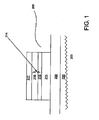
- FIG. 1 shows a cross-sectional view of an embodiment of an electroluminescent (EL) device 200 according to at least one embodiment of the invention.
- the EL device 200 includes an OLED device 205.
- OLED device 205 includes substrate 208 and a first electrode 211 on the substrate 208.
- the first electrode 211 may be patterned for pixilated applications or un-patterned for backlight or other general lighting applications.
- the OLED device 205 also includes a semiconductor stack 214 on the first electrode 211.
- the semiconductor stack 214 includes at least the following: (1) a hole injection layer/anode buffer layer (HIL/ABL) 215 and (2) an active light emitting layer (EML) 216.
- HIL/ABL hole injection layer/anode buffer layer
- EML active light emitting layer
- the OLED device 205 is a bottom-emitting device.
- the first electrode 211 acts as an anode
- the HIL/ABL 215 is deposited onto the first electrode 211
- the EML 216 is deposited onto the HIL/ABL 215.
- the OLED device 205 also includes a second electrode 217 deposited onto the organic semiconductor stack 214.
- Other layers than that shown in FIG. 1 may also be added such as insulating layers, barrier layers, electron/hole injection and blocking layers, getter layers, and so on.
- a layer 230 is disposed on the outside of the OLED device 205. More specifically, in the configuration shown, the refractive layer 230 is disposed on the substrate 208.
- the OLED device 205 and the refractive layer 230 together comprise the EL device 200. Exemplary embodiments of these layers are described in greater detail below.
- the substrate 208 can be any material, which can support the additional layers and electrodes, and is transparent or semi-transparent to the wavelength of light emitted by the OLED device 205.
- Preferable substrate materials include glass, quartz, and plastic, preferably, thin, flexible glass.
- the preferred thickness of the substrate 208 depends on the material used and on the application of the device.
- the substrate 208 can be in the form of a sheet or Continuous film. The continuous film is used, for example, for roll-to-roll manufacturing processes which are particularly suited for plastic, metal, and metallized plastic foils.
- the first electrode 211 functions as an anode (the anode is a conductive layer which serves as a hole-injecting layer).
- Typical anode materials include metals (such as platinum, gold, palladium, indium, and the like); conductive oxides (such as lead oxide, tin oxide, indium-tin oxide, and the like); graphite; and doped conducting polymers (such as polyaniline, polypyrrole, polythiophene, and the like).
- the first electrode 211 is comprised of indium-tin oxide (ITO).
- the first electrode layer 211 can typically be fabricated using any of the techniques known in the art for deposition of thin films, including, for example, vacuum evaporation, sputtering, electron beam deposition, or chemical vapor deposition.
- the HIL/ABL 215 has good hole conducting properties and is used to effectively inject holes from the first electrode 211 to the EML 216.
- the HIL/ABL 215 is made of polymers or small molecule materials or other material.
- the FIIL/ABL 215 can be made from tertiary amine or carbazole derivatives both in their small molecule or their polymer form, conducting polyaniline (“PANI”), or PEDOT:PSS (a solution of poly(3,4-ethylenedioxythiophene) (“PEDOT”) and polystyrenesulfonic acid (“PSS”) (available as Baytron P from HC Starck).
- the HIL/ABL 215 can have a thickness from about 5 nm to about 1000 nm, and is conventionally used from about 50 to about 250 nm.
- HIL/ABL 215 examples include copper phthalocyanine (CuPc) films with preferred thicknesses between 10 and 50 run.
- CuPc copper phthalocyanine
- the HIL/ABL 215 can be formed using selective deposition techniques or nonselective deposition techniques.
- selective deposition techniques include, for example, ink jet printing, flex printing, and screen printing.
- nonselective deposition techniques include, for example, spin coating, dip coating, web coating, and spray coating.
- the active light emitting layer (EML) 216 is comprised of an organic electroluminescent material which emits light upon application of a potential across first electrode 211 and second electrode 217.
- the EML may be fabricated from materials organic or organo-metallic in nature. As used herein, the term organic also includes organo-metallic materials. Light-emission in these materials may be generated as a result of fluorescence or phosphorescence.
- the EML 216 can be a continuous film that is non-selectively deposited (e.g. spin-coating, dip coating etc.) or discontinuous regions that are selectively deposited (e.g. by ink-jet printing). EML 216 may also be fabricated by vapor deposition, sputtering, vacuum deposition etc. as desired.
- the EML 216 can be composed of at least two light emitting elements chosen (i.e. host and dopant). In the case of two light-emitting elements, the relative concentration of the host element and the dopant element can be adjusted to obtain the desired color.
- the EML 216 can emit light in any desired color and be comprised of polymers, co-polymers, dopants, quenchers, and hole and electron transport materials as desired. For instance, the EML 216 can emit light in blue, red, green, orange, yellow or any desired combination of these colors and in some applications, may include a combination of emitting elements which produce white light.
- EML 216 can also include materials capable of charge transport.
- Charge transport materials include polymers or small molecules Chat can transport charge carriers.
- organic materials such as polythiophene, derivatized polythiophene, oligomeric polythiophene, derivatized oligomeric polythiophene, pentacene, triphenylainine, and triphenyldiamine.
- the second electrode 217 functions as the cathode (i.e. as the conductive layer which serves as an electron-injecting layer and which is comprised of a material with a low work function).
- OLED device 205 as shown is a bottom-emitting OLED, and thus, the light emitted from the EML 217 passes through the substrate 208.
- a microstructured film 230 is disposed on the exposed external side of the substrate 208 (and thus, on the exterior of the OLED device 205) to enhance the total light output from EL device 200.
- the microstructured film has prismatic features on the side external to the device. These prismatic features serve to diffuse light emitted by OLED device 205.
- the microstructured film splits the image from one stripe into two or more images.
- the "split" images from adjacent stripes blend together to yield a broader color spectrum.
- the chemical composition of the microstructured film 230 will depend at least in part upon the properties, e.g. the refractive index, of the substrate 208 from which light is passed to the microstructured film 230.
- the refractive index of the microstructured film 230 is preferably at or about 1.48 to optimize the out-coupling of light from the substrate into the refractive film.
- Commercially available microstructured films based on polycarbonate have a refractive index in the range of 1.5 to 1.6 which would be suitable for a glass substrate, for example.
- One example is a film called BEF III available from 3M Corporation which is made of a modified acrylic resin backed upon polyester. BEF III has a microreplicated prismatic structure.
- the geometry of the microstructures on the film can be any suitable geometry to achieve diffusion or refraction of light.
- the microstructured film 230 itself may have a thickness ranging from about 50 to 400 micrometers and in some embodiments around the 150-160 micrometer range.
- the microstructured film 230 can be attached to the substrate 208 using an optically adhesive glue, which may additionally also be curable by ultraviolet radiation, or an index matching gel.
- the microstructured film 230 can be deposited or formed directly on substrate 208. Further, the microstructured film 230 can utilize a cross-linkable material which can then be chemically bonded to the substrate 208.
- FIG. 6 below and the associated description detail the characteristics of microstructured films as utilized in various embodiments of the invention.
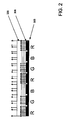
- FIG. 2 shows a cross-sectional view of exemplary striped light emission in accordance with at least one embodiment of the invention.
- Exemplary light rays are shown emerging from an OLED display 305.
- OLED display 305 is a matrix of OLED devices with a portion of the devices emitting in red (R), a portion emitting in green (G) and a portion emitting in blue (B).
- Emitted light from each stripe passes through substrate 308.
- a microstructured film 308 is attached to the substrate 308.
- the emitted light from each R, G and B stripe is diffused by film 330 into the emissive area of adjacent stripes when the stripes of the prism in the film 330 run parallel to the emissive stripes of the device.
- the emission from the R stripes is shown split and diffused into the area where neighboring stripes emit.
- the emission from the C stripe is also diffused into the area where its neighboring stripes emit.
- a similar splitting effect would occur with respect to the emission from the R stripe as well.
- the blending of emitted light in this fashion can produce a broader spectrum which is also more uniform in color appearance across the display.
- By blending the light of the three basic colors red, green and blue in different intensities it is possible to produce any nuance of color. This enables a color tunable light source using the diffusing properties to blend the emitted colors.
- FIG. 3 illustrates the measuring zones for FIG. 4 and FIG. 5.
- An OLED lighting source was partitioned into three zones.
- Zone 1 is a blank domain without any microstructured film.
- Zone 2 is a domain wherein a microstructured film was applied on the substrate of the OLED lighting source.
- Zone 3 is a cross-section through both of these domains where the luminance was measured.
- FIG. 4 illustrates the luminance (brightness) for a striped OLED device emitting every third stripe using the measurement system shown in FIG. 3. shows the luminance of striped OLED panel with only 'green' switched on (i.e. only every third stripe is emitting).
- the average luminance for zone 2 (which includes a microstructured film) was around 350 nits while the average luminance for zone 1 (same emission without a microstructured film) was around 271 nits. This is an improvement in average luminance of about 29%. Even though the peak luminance at selected locations was greater in zone 1, there were better more uniform luminance levels over a larger area in zone 2 and few large drops in luminance.
- the luminance levels rarely if ever dropped below 200 nits over the entire zone 2 area whereas in the zone 1 area luminance levels often drop under 100 and near 50 nits.
- This flattening of the luminance profile over the area of the display is due to the diffusive effect of the microstructured film. There is significant emission of even in areas where the corresponding underlying stripe is not emitting.
- FIG. 5 illustrates the luminance for a striped OLED display emitting in all stripes using the measurement system shown in FIG. 3.
- a white emitting OLED display was measured with all stripes emitting. With all stripes emitting, there is an increase in average luminance as well an increase in luminance at given measured locations (peak luminance at each location)
- the average luminance for zone 2 (which includes a microstructured film) was around 488 nits while the average luminance for zone 1 (same emission without a microstructured film) was around 359 nits. This is an improvement in average luminance of about 35%.
- the peak luminance at selected locations was greater in zone 2, and there were more uniform and larger luminance levels over a larger area in zone 2 and few significant drops in luminance from one measured location to the next. For instance, the luminance levels rarely if ever dropped below 400 nits over the entire zone 2 area whereas in the zone 1. This flattening of the luminance profile over the area of the display is due to the diffusive effect of the microstructured film. There is a more uniform luminance profile due to the blending of light from adjacent emitting stripes.
- FIG. 6 illustrates a microstructured film in accordance with one or more embodiments of the invention.
- the invention comprises at least one microstructured film 600 which is fabricated and disposed over and on the outside of a substrate of a bottom-emitting OLED device/display.
- the microstructured film 600 is thus attached to the outside of the OLED device/display and not included as a part of the device/display. In this way, such a layer can be used on any OLED or similar lighting device/display independent of internal device structure.
- the microscructured film 600 is placed in the path of light emission and thus, on the outside of the OLED device and on the outside of the substrate (bottom-emitting).
- the microstructured film 600 has periodic or aperiodic and random features prismatic or otherwise lens-like which serve to diffuse light.
- the features may also be rounded and more smooth at peak like waves of water rather than with sharp features and angles found in a prismatic structure.
- the features on the surface of the film 600 are on the side distal to the side of attachment to the OLED device/display.
- the features are aligned in a "row" (the direction of the row indicated by the arrows in FIG. 6) and the rows are repetitively placed across the width of the film 600.
- the stripes of a striped OLED device are parallel to the feature rows on the microstructured film. The direction in which this parallel alignment would be made is indicated in the arrows on FIG. 6.
- the width of features (from row to row, peak to peak as indicated in FIG. 6) is about 1/10 th the width of an individual OLED stripe.
- the width of a row is much smaller than the width of an OLED stripe such that many features can be utilized to diffuse the emission of a single stripe.
- the width of the a row may be the same or greater than the width of a single stripe.
- the feature size, row size and period of the features on the film can be any suitable range and the ranges given above are merely exemplary.
- the first electrode 211 functions as a cathode (the cathode is a conductive layer which serves as an electron-injecting layer and which comprises a material with a low work function).
- the cathode rather than the anode, is deposited on the substrate 208 in the case of a top-emitting OLED.
- the second electrode layer 217 functions as an anode (the anode is a conductive layer which serves as a hole-injecting layer and which comprises a material with work function greater than about 4.5 eV).
- the anode, rather than the cathode is deposited on the semiconductor stack 214 in the case of a top-emitting OLED.
- the anode may be made transparent or translucent to allow light to pass from the semiconductor stack 214 through the top of the device.
- the microstructured film 600 would be attached, bonded or cured to the anode 217 (or to a glass or other material which encapsulates and protects the anode) rather than to the substrate 208 as with a bottom-emitting OLED shown in FIG. 2.
- OLED lighting sources and displays produced from a combination or arrays of OLED devices described earlier can be used within applications such as information displays in vehicles, industrial and area lighting, telephones, printers, and illuminated signs.
Landscapes
- Physics & Mathematics (AREA)
- Optics & Photonics (AREA)
- Electroluminescent Light Sources (AREA)
Applications Claiming Priority (1)
| Application Number | Priority Date | Filing Date | Title |
|---|---|---|---|
| US11/215,548 US7586245B2 (en) | 2005-08-29 | 2005-08-29 | Using prismatic microstructured films for image blending in OLEDS |
Publications (1)
| Publication Number | Publication Date |
|---|---|
| EP1760801A2 true EP1760801A2 (fr) | 2007-03-07 |
Family
ID=37467512
Family Applications (1)
| Application Number | Title | Priority Date | Filing Date |
|---|---|---|---|
| EP06018045A Withdrawn EP1760801A2 (fr) | 2005-08-29 | 2006-08-29 | Films prismatiques microstructurés utilisés pour l'insertion d'images des OLEDs |
Country Status (2)
| Country | Link |
|---|---|
| US (1) | US7586245B2 (fr) |
| EP (1) | EP1760801A2 (fr) |
Families Citing this family (9)
| Publication number | Priority date | Publication date | Assignee | Title |
|---|---|---|---|---|
| US7586245B2 (en) | 2005-08-29 | 2009-09-08 | Osram Opto Semiconductors Gmbh | Using prismatic microstructured films for image blending in OLEDS |
| US8330348B2 (en) * | 2005-10-31 | 2012-12-11 | Osram Opto Semiconductors Gmbh | Structured luminescence conversion layer |
| US7321193B2 (en) * | 2005-10-31 | 2008-01-22 | Osram Opto Semiconductors Gmbh | Device structure for OLED light device having multi element light extraction and luminescence conversion layer |
| US7420323B2 (en) * | 2005-10-31 | 2008-09-02 | Osram Opto Semiconductors Gmbh | Electroluminescent apparatus having a structured luminescence conversion layer |
| US20110157893A1 (en) * | 2009-12-28 | 2011-06-30 | Ngai Peter Y Y | Oled luminaire having observable surfaces with differential visual effects |
| TW201245405A (en) * | 2011-03-08 | 2012-11-16 | Du Pont | Organic electronic device for lighting |
| KR101818033B1 (ko) * | 2011-11-01 | 2018-01-16 | 한국전자통신연구원 | 플렉시블 전극 기판의 제조방법 |
| KR102120808B1 (ko) * | 2013-10-15 | 2020-06-09 | 삼성전자주식회사 | 색 변화 저감용 광학 필름 및 이를 채용한 유기 발광 표시 장치 |
| KR102099781B1 (ko) * | 2013-10-15 | 2020-04-10 | 삼성전자주식회사 | 색 변화 저감용 광학 필름 및 이를 채용한 유기 발광 표시 장치 |
Family Cites Families (27)
| Publication number | Priority date | Publication date | Assignee | Title |
|---|---|---|---|---|
| DE29724847U1 (de) * | 1996-06-26 | 2004-09-30 | Osram Opto Semiconductors Gmbh | Lichtabstrahlendes Halbleiterbauelement mit Lumineszenzkonversionselement |
| TW420965B (en) * | 1998-07-14 | 2001-02-01 | Matsushita Electric Industrial Co Ltd | Dispersion-type electroluminescence element |
| US6771019B1 (en) * | 1999-05-14 | 2004-08-03 | Ifire Technology, Inc. | Electroluminescent laminate with patterned phosphor structure and thick film dielectric with improved dielectric properties |
| JP4432171B2 (ja) | 1999-11-22 | 2010-03-17 | 凸版印刷株式会社 | 有機エレクトロルミネッセンス表示素子およびその製造方法 |
| US7233026B2 (en) * | 2000-03-23 | 2007-06-19 | Emagin Corporation | Light extraction from color changing medium layers in organic light emitting diode devices |
| JP2001284576A (ja) * | 2000-03-30 | 2001-10-12 | Toshiba Corp | 高電子移動度トランジスタ及びその製造方法 |
| US6777871B2 (en) * | 2000-03-31 | 2004-08-17 | General Electric Company | Organic electroluminescent devices with enhanced light extraction |
| US6747405B2 (en) * | 2000-11-28 | 2004-06-08 | Demitsu Kosan Co., Ltd. | Organic EL display device having conductive color changing layers |
| US6984934B2 (en) * | 2001-07-10 | 2006-01-10 | The Trustees Of Princeton University | Micro-lens arrays for display intensity enhancement |
| JP2003115377A (ja) * | 2001-10-03 | 2003-04-18 | Nec Corp | 発光素子、その製造方法およびこれを用いた表示装置 |
| US6903505B2 (en) * | 2001-12-17 | 2005-06-07 | General Electric Company | Light-emitting device with organic electroluminescent material and photoluminescent materials |
| US6833667B2 (en) * | 2002-02-27 | 2004-12-21 | Matsushita Electric Industrial Co., Ltd. | Organic electroluminescence element and image forming apparatus or portable terminal unit using thereof |
| US6703781B2 (en) * | 2002-05-21 | 2004-03-09 | Durel Corporation | El lamp with light scattering particles in cascading layer |
| US7015640B2 (en) * | 2002-09-11 | 2006-03-21 | General Electric Company | Diffusion barrier coatings having graded compositions and devices incorporating the same |
| US6965197B2 (en) * | 2002-10-01 | 2005-11-15 | Eastman Kodak Company | Organic light-emitting device having enhanced light extraction efficiency |
| US7554258B2 (en) * | 2002-10-22 | 2009-06-30 | Osram Opto Semiconductors Gmbh | Light source having an LED and a luminescence conversion body and method for producing the luminescence conversion body |
| US20060003477A1 (en) | 2002-10-30 | 2006-01-05 | Bert Braune | Method for producing a light source provided with electroluminescent diodes and comprising a luminescence conversion element |
| JP2004241130A (ja) * | 2003-02-03 | 2004-08-26 | Seiko Epson Corp | 発光ディスプレイパネルおよびその製造方法 |
| US7229703B2 (en) * | 2003-03-31 | 2007-06-12 | Dai Nippon Printing Co. Ltd. | Gas barrier substrate |
| US7030555B2 (en) * | 2003-04-04 | 2006-04-18 | Nitto Denko Corporation | Organic electroluminescence device, planar light source and display device using the same |
| US20040217702A1 (en) * | 2003-05-02 | 2004-11-04 | Garner Sean M. | Light extraction designs for organic light emitting diodes |
| JP2005050708A (ja) * | 2003-07-29 | 2005-02-24 | Samsung Sdi Co Ltd | 光学素子用基板及び有機エレクトロルミネッセンス素子並びに有機エレクトロルミネッセンス表示装置 |
| KR20050066970A (ko) * | 2003-12-26 | 2005-06-30 | 닛토덴코 가부시키가이샤 | 전자발광 장치, 이를 사용하는 면광원 및 디스플레이 |
| US7252893B2 (en) * | 2004-02-17 | 2007-08-07 | Eastman Kodak Company | Anthracene derivative host having ranges of dopants |
| KR20050099260A (ko) * | 2004-04-09 | 2005-10-13 | 삼성전자주식회사 | 플라즈마 디스플레이 패널 |
| US7602118B2 (en) * | 2005-02-24 | 2009-10-13 | Eastman Kodak Company | OLED device having improved light output |
| US7586245B2 (en) | 2005-08-29 | 2009-09-08 | Osram Opto Semiconductors Gmbh | Using prismatic microstructured films for image blending in OLEDS |
-
2005
- 2005-08-29 US US11/215,548 patent/US7586245B2/en active Active
-
2006
- 2006-08-29 EP EP06018045A patent/EP1760801A2/fr not_active Withdrawn
Also Published As
| Publication number | Publication date |
|---|---|
| US20070046161A1 (en) | 2007-03-01 |
| US7586245B2 (en) | 2009-09-08 |
Similar Documents
| Publication | Publication Date | Title |
|---|---|---|
| US7321193B2 (en) | Device structure for OLED light device having multi element light extraction and luminescence conversion layer | |
| US7420323B2 (en) | Electroluminescent apparatus having a structured luminescence conversion layer | |
| US7504770B2 (en) | Enhancement of light extraction with cavity and surface modification | |
| CN100573639C (zh) | 光电显示器 | |
| JP5793421B2 (ja) | 極薄多基板調色oledデバイス | |
| JP2006245003A (ja) | エレクトロルミネセンス装置 | |
| US7586245B2 (en) | Using prismatic microstructured films for image blending in OLEDS | |
| US20070176539A1 (en) | OLED with area defined multicolor emission within a single lighting element | |
| KR101366655B1 (ko) | 유기 전자 장치들의 처리 및 성능을 개선하기 위한중성화된 애노드 버퍼층들 | |
| KR100970482B1 (ko) | 유기 발광소자 및 그 제조방법 | |
| JP2005531899A (ja) | 透明な陰極を備える電場発光装置 | |
| CN100468814C (zh) | 有机发光显示器 | |
| US20070188086A1 (en) | Light souce | |
| US20060290272A1 (en) | Enhancement of light extraction using gel layers with excavations | |
| US8232721B2 (en) | Efficiency enhancement methods for OLED light source through index bridging | |
| US20080259987A1 (en) | Enhanced Emission of Light From Organic Light Emitting Diodes | |
| US7521856B2 (en) | OLED device | |
| Wenke | Organic light emitting diode (oled) | |
| US20050064234A1 (en) | Emissive polymer layer | |
| CN100433400C (zh) | 有机高分子发光二极管装置及其应用的显示器 | |
| US20060147749A1 (en) | Organic polymer light emitting diode device and applied display | |
| KR200330895Y1 (ko) | 유기 전계 발광 소자 | |
| WO2020226051A1 (fr) | Dispositif électroluminescent (el) organique | |
| EP2144310A1 (fr) | Dispositif électroluminescent | |
| KR20050024376A (ko) | 컬러 필터를 갖는 전자발광 디바이스 |
Legal Events
| Date | Code | Title | Description |
|---|---|---|---|
| PUAI | Public reference made under article 153(3) epc to a published international application that has entered the european phase |
Free format text: ORIGINAL CODE: 0009012 |
|
| AK | Designated contracting states |
Kind code of ref document: A2 Designated state(s): AT BE BG CH CY CZ DE DK EE ES FI FR GB GR HU IE IS IT LI LT LU LV MC NL PL PT RO SE SI SK TR |
|
| AX | Request for extension of the european patent |
Extension state: AL BA HR MK YU |
|
| RAP1 | Party data changed (applicant data changed or rights of an application transferred) |
Owner name: OSRAM OPTO SEMICONDUCTORS GMBH |
|
| RAP1 | Party data changed (applicant data changed or rights of an application transferred) |
Owner name: OSRAM OPTO SEMICONDUCTORS GMBH |
|
| STAA | Information on the status of an ep patent application or granted ep patent |
Free format text: STATUS: THE APPLICATION IS DEEMED TO BE WITHDRAWN |
|
| 18D | Application deemed to be withdrawn |
Effective date: 20100302 |