EP1760831B1 - Antenne planaire - Google Patents
Antenne planaire Download PDFInfo
- Publication number
- EP1760831B1 EP1760831B1 EP05025972A EP05025972A EP1760831B1 EP 1760831 B1 EP1760831 B1 EP 1760831B1 EP 05025972 A EP05025972 A EP 05025972A EP 05025972 A EP05025972 A EP 05025972A EP 1760831 B1 EP1760831 B1 EP 1760831B1
- Authority
- EP
- European Patent Office
- Prior art keywords
- loop
- antenna
- antenna element
- shaped
- power
- Prior art date
- Legal status (The legal status is an assumption and is not a legal conclusion. Google has not performed a legal analysis and makes no representation as to the accuracy of the status listed.)
- Expired - Lifetime
Links
Images






Classifications
-
- H—ELECTRICITY
- H01—ELECTRIC ELEMENTS
- H01Q—ANTENNAS, i.e. RADIO AERIALS
- H01Q1/00—Details of, or arrangements associated with, antennas
- H01Q1/27—Adaptation for use in or on movable bodies
- H01Q1/32—Adaptation for use in or on road or rail vehicles
-
- H—ELECTRICITY
- H01—ELECTRIC ELEMENTS
- H01Q—ANTENNAS, i.e. RADIO AERIALS
- H01Q21/00—Antenna arrays or systems
- H01Q21/24—Combinations of antenna units polarised in different directions for transmitting or receiving circularly and elliptically polarised waves or waves linearly polarised in any direction
-
- H—ELECTRICITY
- H01—ELECTRIC ELEMENTS
- H01Q—ANTENNAS, i.e. RADIO AERIALS
- H01Q7/00—Loop antennas with a substantially uniform current distribution around the loop and having a directional radiation pattern in a plane perpendicular to the plane of the loop
-
- H—ELECTRICITY
- H01—ELECTRIC ELEMENTS
- H01Q—ANTENNAS, i.e. RADIO AERIALS
- H01Q9/00—Electrically-short antennas having dimensions not more than twice the operating wavelength and consisting of conductive active radiating elements
- H01Q9/04—Resonant antennas
- H01Q9/16—Resonant antennas with feed intermediate between the extremities of the antenna, e.g. centre-fed dipole
-
- H—ELECTRICITY
- H01—ELECTRIC ELEMENTS
- H01Q—ANTENNAS, i.e. RADIO AERIALS
- H01Q9/00—Electrically-short antennas having dimensions not more than twice the operating wavelength and consisting of conductive active radiating elements
- H01Q9/04—Resonant antennas
- H01Q9/16—Resonant antennas with feed intermediate between the extremities of the antenna, e.g. centre-fed dipole
- H01Q9/26—Resonant antennas with feed intermediate between the extremities of the antenna, e.g. centre-fed dipole with folded element or elements, the folded parts being spaced apart a small fraction of operating wavelength
Definitions
- the present invention relates to a planar antenna.
- the invention relates particularly to an art suitable for use as an antenna which is formed on a dielectric substate to generate circularly polarized waves.
- ETC Electronic Toll Collection
- VICS Vehicle Information Communications System
- circularly polarized waves are used in GPS radio waves, satellite radio waves for satellite broadcasting, and ETC radio waves.
- Most of the previous antennas for circularly polarized waves are patch antennas (planar antenna).
- FIG. 11 is a schematic plan view showing a construction of an example of a previous planar antenna, and it is disclosed in the following patent document 1.
- the planar antenna of FIG. 11 which is for receiving right-hand circularly polarized waves, includes a square-like loop antenna (power-fed element) 120 and a linear electric conductor [parasitic (non-power-supplied) element] 140 mounted on a dielectric (transparent film).
- the linear electric conductor 140 which is an independent conductor not coupled to the loop antenna 120, is bent to be divided into two parts, a first part 140A and a second part 140B.
- Reference characters 160 and 170 designate power-feeding terminals for supplying the loop antenna 120 with electric power; reference character 270 designates connecting conductors which connect power-feeding terminals 160 and 170 to the loop antenna 120; reference character CP designates the center point of the loop antenna 120.
- the parasitic element 140 is placed outside the loop antenna 120 and is arranged close to the loop antenna 120.
- the first part 140A is placed in parallel with one side of the loop antenna 120; the second part 140B is placed in parallel with a straight line which connects an intermediate point between the power-feeding terminals 160 and 170 and an apex of the loop antenna 120 which is opposite the intermediate point.
- a loop antenna 120 without a parasitic element 140 in particular, a loop antenna 120 whose circumference (the total length of the antenna conductor) is equal to one wavelength, can receive only an electric field component (lateral component) in the horizontal direction (that is, it is impossible to completely receive circularly polarized waves in which the direction of the electric field changes over time).
- the parasitic element 140 arranged close to the loop antenna 120 makes it possible for the loop antenna 120 to receive a vertical component of the circularly polarized waves.
- the secondpart 140B of the parasitic element 140 takes in the vertical component of the circularly polarized waves, and this received vertical component is coupled to the antenna conductor of the loop antenna 120 by the first part 140A which is close to the antenna conductor of the loop antenna 120.
- the vertical and lateral components of the circularly polarized waves are received by the loop antenna 120 in phase.
- the parasitic element 140 is provided with the first part 140A.
- Patent document 2 relates to a thin and flat antenna construction including more than one stacked loop antenna element.
- the antenna of patent document 2 is capable of generating left-hand circularly polarized waves and right-hand circularly polarized waves at the same time from two directions.
- Patent document 3 relates to an antenna construction in which a large square row antenna is provided in the plane of an antenna. Inside the large antenna, a small dipole antenna, a loop antenna, and a planar antenna are arranged so that the directivities of the antennas formed by interference of the antennas are optimum.
- patent document 1 is disadvantageous in that electric field distribution to they parasitic element 140 is weak due to the antenna construction, so that it is difficult to obtain a sufficiently good circular polarization characteristic. This is probably because a linear antenna (e.g. , a dipole antenna) simply mounted on a dielectric substrate generates a beam in the direction along the surface of the dielectric substrate, so that the intensity of radiation in the direction (that is, the direction along the thickness) crossing the surface of the dielectric substrate is weak.
- a linear antenna e.g. , a dipole antenna
- patent document 2 the purpose of the art of patent document 2 is generating left-hand and right-hand circularly polarized waves at the same time.
- patent document 3 it is possible to place multiple antennas closely or concentratedly in a narrow area, and thus down-sizing is available, and the purpose of the invention is to prevent noise from inside automobiles. Therefore, neither of the applications aims at obtaining a good circular polarization characteristic.
- Patent document GB 2 111 756 A relates to improvements in the directivity and gain of an antenna element associated with a finite length reflector, which has a wide angle directivity.
- a feed antenna such as dipole antenna is surrounded by a non-feed element loop element within the same imaginary plane and which is additionally arranged with a reflector that the non-feed loop could be formed on a dielectric body.
- Patent document JP 07 2499921 A relates to a plane antenna appropriate for receiving satellite broadcasting by a circularly polarized wave.
- a parasitic element is arranged on the front face of a loop like antenna element.
- Patent document JP 2005 167619 A relates to a plate like conductor pattern usable for a glass antenna.
- the present invention provides a planar antenna with simple configuration which realizes a good circular polarization characteristic.
- the application of the present invention should by no means be limited to movable objects such as automobiles, and the present invention is applicable also to POS systems and security systems for preventing product theft.
- planar antenna of the present invention simple antenna patterns (a power-fed linear antenna element or a power-fed loop-shaped antenna element and a parasitic loop-shaped antenna element) formed on one surface of the dielectric substrate are capable of producing circularly polarized waves with good characteristics on the opposite sides of the dielectric substrate. Accordingly, it is possible for the planar antenna of the present invention to efficiently receive circularly polarized waves in which the direction of the electric field changes over time, such as radio waves for GPS, satellite radio waves for satellite digital broadcasting, and radio waves for ETC, so that the reception characteristic of the circularly polarized waves is improved.
- FIG. 1 is a schematic plan view showing a construction of a planar antenna according to a first embodiment of the present invention.
- a dipole antenna element (linear antenna element) 1 which is a linear antenna conductor supplied with electric power (power-fed) from a feeding point 1e, is formed on one side of a dielectric substrate (hereinafter will be simply called the “dielectric" or “substrate") 10, which is made of, for example, glass or ceramic.
- the substrate can be divided into two areas (divisional areas) with the dipole antenna element 1 as a boundary. In one of the two divisions (the part above the dipole antenna element 1 of FIG.
- a first loop antenna element (a parasitic loop-shaped antenna element serving as an electromagnetic coupling loop) which is not supplied with electric power and is loop-shaped (rectangular shape) 2 is formed in the vicinity of one end 1a of the dipole antenna element 1.
- the first loop antenna element 2 is placed in such a manner that one of its short sides is positioned in the proximity of one end 1a of the dipole antenna element 1, and that its long sides extend in the direction (+y-axis direction) which crosses the dipole antenna element 1 in the substrate plane (x-y plane).
- the other divisional area (the side lower than the dipole antenna element 1 of FIG.
- a second loop antenna element (a parasitic loop-shaped antenna element serving as an electromagnetic coupling loop) 3 which is not supplied with electric power and is loop-shaped (rectangular shape) 2 is formed in the vicinity of the other end 1b of the dipole antenna element 1.
- the second loop antenna element 3 is placed in such a manner that one of its short sides is positioned in the proximity of the other end 1b of the dipole antenna element 1, and that its long sides extend in the direction (-y-axis direction) which crosses the dipole antenna element 1 in the substrate plane.
- the loop antenna elements 2 and 3 are formed/placed in the vicinity of the dipole antenna element 1, symmetrically with respect to the center point of the dipole antenna element 1, so that the loop antenna elements 2 and 3 can be electromagnetically coupled to the dipole antenna element 1.
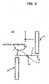
- the reason why the loop antenna elements 2 and 3 are placed in the vicinity of the opposite ends 1a and 1b of the dipole antenna element 1 is that in the distribution of voltage of a dipole antenna element 1, the voltage value (absolute value) becomes greater at positions closer to the opposite ends 1a and 1b, away from the center (in the proximity of the feeding point 1e) of the dipole antenna element 1 (the value takes the maximum value at opposite ends 1a and 1b), as shown in FIG. 2 with reference character 20, resulting in good coupling efficiency.
- the dipole antenna element 1 If electric power is supplied to the dipole antenna element 1 under such an antenna construction, an electric field is radiated in the z-axis direction (the vertical direction relative to the paper sheet of FIG. 1 ) so that the dipole antenna element 1 has a first cross polarization component, and each of the loop antenna elements 2 and 3 has a second cross polarization component whose phase is delayed by 90° in comparison with the first cross polarization component and polarization is also different from that of the first cross polarization component by 90°.
- the dipole antenna element 1 generates an electric field (E x field) having a polarization component (horizontal polarization) in the x-axis direction, and the electric field is coupled to each of the loop antenna elements 2 and 3, whereby electric current flows in the loop antenna elements 2 and 3.
- E x field an electric field having a polarization component (horizontal polarization) in the x-axis direction
- the electric field is coupled to each of the loop antenna elements 2 and 3, whereby electric current flows in the loop antenna elements 2 and 3.
- an electric field (E y field) has a strong polarization component (vertical polarization) in the y-axis direction in comparison with in the x-axis direction.
- each of the loop antenna elements 2 and 3 has a rectangular shape having linear portions (long sides) thereof extending in the direction which crosses the dipole antenna element 1, so as to produce the vertical polarization.
- the size of the dielectric substrate 10 is 300 mm (vertical length) ⁇ 300 mm (lateral length) ⁇ 6 mm (thickness); the dielectric constant ⁇ r is 7; the conductivity of the dipole antenna element 1 and of the loop antenna elements 2 and 3 is 5 ⁇ 10 6 , the length of the dipole antenna element 1 is a half-wavelength ( ⁇ /2) of the wavelength ⁇ of a radio signal to be transceived (for example, 97.4 mm) ; the lengths of the long and the short sides of each of the loop antenna elements 2 and 3 are 95 mm and 15 mm, respectively (95 mm ⁇ 15 mm), so that the total loop length is 220 mm; each of the loop antenna elements 2 and 3 are placed at a position approximately 7 mm away from the dipole antenna element 1 in the y-axis direction, and approximately 33 mm away from the center point of the dipole antenna element 1. With this construction, if power is supplied to the dipole antenna element 1 by
- FIG. 3 shows a three-dimensional power gain radiation pattern of the above planar antenna
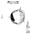
- FIG. 4 shows a three-dimensional right-hand circular polarization gain radiation pattern of the above planar antenna
- FIG. 5 shows a two-dimensional (the x-z plane, that is, the plane along the power-supplied dipole antenna 1) right-hand circular polarization gain radiation pattern of the above planar antenna
- FIG. 6 shows a two-dimensional (the y-z plane, that is, the plane orthogonal to the dipole antenna element 1) right-hand circular polarization gain radiation pattern of the planar antenna.
- simple antenna elements 1, 2, and 3 (conductor patterns) formed on one surface of the dielectric substrate 10 are capable of producing circularly polarized waves with good characteristics on the opposite sides of the dielectric substrate 10.
- the loop antenna elements 2 and 3 should be placed at opposite sides relative to the dipole antenna element 1 (at symmetric positions opposite to those of FIG. 1 ).
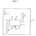
- FIG. 7 is a schematic plan view showing a construction of a planar antenna according to a second embodiment of the present invention.
- a four-sided (rectangular) loop antenna element (power-fed loop-shaped antenna element) 1A which is supplied with electric power (power-fed) from a feeding point 1e, is formed on one surface (x-y plane) of a dielectric substrate 10, which is made of, for example, glass or ceramic.
- a parasitic rectangular loop antenna element (an antenna conductor serving as an electromagnetic coupling loop) 2 is placed in the vicinity of one side 11 of the two opposite (in the x-axis direction) sides (short sides) of the power-fed loop antenna element 1A, and the long sides of the loop antenna element 2 extend in the y-axis direction.
- another parasitic rectangular loop antenna element (an antenna conductor serving as an electromagnetic coupling loop) 3 is placed in the vicinity of the other side 12, and the long sides of the loop antenna element 3 extend in the y-axis direction.
- the loop antenna elements 2 and 3 are placed outside the loop antenna element 1A in the vicinity of the loop antenna element 1A, and they are arranged symmetrically with respect to the center point of the loop antenna element 1A. With this arrangement, the loop antenna elements 2 and 3 canbe electromagnetically coupled to the loop antenna element 1A via the sides 11 and 12.
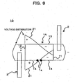
- the positions at which the loop antenna elements 2 and 3 are placed are determined based on the voltage distribution formed by the loop antenna element 1A. More specifically, when the loop antenna element 1A is supplied with electric power, a voltage distribution shown in FIG. 8 with the reference character 21 is revealed. The voltage value (absolute value) on one long side 13 (the side opposite the feeding point 1e) of the loop antenna element 1A becomes greater at positions closer to the opposite ends of the long side 13, away from in the vicinity of the center of the long side 13.
- the voltage value (absolute value) on the other long side 14 (the side on which the feeding point 1e exists) of the loop antenna element 1A becomes greater at positions closer to the opposite ends of the long side 14, away from in the vicinity of the center of the long side 14.
- the loop antenna elements 2 and 3 are placed in the vicinity of the sides 11 and 12 so that at least a portion (a portion of each long side) of the loop antenna elements 2 and 3 faces one of the line segments obtained by dividing the sides 11 and 12 into two equal parts.
- an electric field (E x field) having a strong polarization (horizontal polarization) component in the x-axis direction is produced because the sides 13 and 14 are longer than the sides 11 and 12.
- the electric field is coupled to the loop antenna elements 2 and 3 via the sides 11 and 12, whereby electric current flows in the loop antenna elements 2 and 3.
- the loop antenna elements 2 and 3 serving as a parasitic loop-shaped antenna element, are arranged so as to produce cross polarized waves (vertically polarized waves) which cross the main polarized waves (horizontally polarized waves) generated by the loop antenna element 1A.
- each of the loop antenna elements 2 and 3 has a rectangular shape having linear portions (long sides) thereof extending in the direction which crosses the dipole antenna element 1, so as to produce vertically polarized waves.
- the intensity and the phase of the cross electric field components which are orthogonal to each other by means of adjusting (i) the shape of the loop antenna elements 2 and 3 (the shape of the portion at which the loop antenna elements 2 and 3 are coupled to the loop antenna element 1A), (ii) the distance in the x-axis direction between the loop antenna element 1A and the loop antenna elements 2 and 3, and (iii) the positions of the loop antenna elements 2 and 3 in the y-axis direction.
- the shape of the loop antenna elements 2 and 3 the shape of the portion at which the loop antenna elements 2 and 3 are coupled to the loop antenna element 1A
- the distance in the x-axis direction between the loop antenna element 1A and the loop antenna elements 2 and 3 and
- simple antenna elements 1A, 2, and 3 (conductor patterns) formed on one surface of the dielectric substrate 10 are capable of producing circularly polarized waves with good characteristics on the opposite sides of the dielectric substrate 10. Accordingly, it is possible to efficiently receive circularly polarized waves in which the direction of the electric field changes over time, such as radio waves for GPS, satellite radio waves for satellite digital broadcasting, and radio waves for ETC, so that the reception characteristic of the circularly polarized waves is improved.
- the loop antenna elements 2 and 3 should be placed at opposite sides relative to the center line of the long axis (x-axis) of the loop antenna element 1A (at symmetric positions opposite to those of FIG. 7 ).
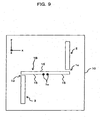
- FIG. 9 is a schematic plan view showing a construction of a planar antenna according to a second embodiment of the present invention.
- a folded dipole antenna element 1B which is supplied with electric power (power-fed) from a feeding point 1e, is formed on one surface (x-y plane) of a dielectric substrate 10, which is made of, for example, glass or ceramic.
- a parasitic rectangular loop antenna element (an antenna conductor serving as an electromagnetic coupling loop) 2 is placed in the vicinity of one side 15 of the two opposite (in the y-axis direction) sides (long sides) 15 and 16 of the antenna element 1B, and the long sides of the loop antenna element 2 extend in the y-axis direction.
- another antenna element (an antenna conductor serving as an electromagnetic coupling loop) 3 is placed in the vicinity of the other side 16, and the long sides of the loop antenna element 3 extend in the y-axis direction.
- the planar antenna of FIG. 9 is equivalent to a construction of FIG. 1 in which the dipole antenna element 1 is replaced by the folded dipole antenna element 1B (hereinafter will be called the "antenna element 1B").
- One loop antenna element 2 of the two loop antenna elements 2 and 3 is formed/placed in the vicinity of one end (folded part) 1c of the long side 15 of the antenna element 1B, and the other loop antenna element 3 is formed/placed in the vicinity of the other end (folded part) 1d of the long side 16 of the folded dipole antenna element 1B.
- the loop antenna elements 2 and 3 are formed/placed in the vicinity of the dipole antenna element 1 symmetrically with respect to the center point of the folded dipole antenna element 1B, so that the loop antenna elements 2 and 3 can be electromagnetically coupled to the antenna element 1B via the sides 15 and 16.
- the positions at which the loop antenna elements 2 and 3 are placed are determined based on the voltage distribution formed by the antenna element 1B. That is, when electric power is supplied to the folded dipole antenna element 1B, the voltage value (absolute value) becomes greater at positions closer to the opposite ends 1c and 1d, away from the center (in the proximity of the feeding point) of the antenna element 1B (the value takes the maximum value at opposite ends 1c and 1d), as shown in FIG. 10 with reference character 23.
- the loop antenna elements 2 and 3 are placed in the vicinity of the ends of the sides 15 and 16 where good coupling efficiency is revealed.
- an electric field (E x field) having a strong polarization (horizontal polarization) component in the x-axis direction is produced by electric current flowing in the long sides 15 and 16, and the electric field is coupled to the loop antenna elements 2 and 3 via the sides 15 and 16, whereby electric current flows in the loop antenna elements 2 and 3.
- the loop antenna elements 2 and 3 serving as a parasitic loop-shaped antenna element, are arranged so as to produce cross polarized waves (vertically polarized waves) which cross the polarized waves (horizontally polarized waves) generated by the folded dipole antenna element 1B.
- each of the loop antenna elements 2 and 3 has a rectangular shape having linear portions (long sides) thereof extending in the direction which crosses the folded dipole antenna element 1B, so as to produce vertically polarized waves.
- simple antenna elements 1B, 2, and 3 (conductor patterns) formed on one surface of the dielectric substrate 10 are capable of producing circularly polarized waves with good characteristics on the opposite sides of the dielectric substrate 10.
- the loop antenna elements 2 and 3 should be placed at opposite sides relative to the center line of the long axis (x-axis) of the antenna element 1B (at symmetric positions opposite to those of FIG. 9 ).
- the parasitic loop-shaped antenna element is placed so as to produce cross polarized waves which cross the polarized waves (main polarized waves) generated by a power-fed linear antenna element or a power-fed loop-shaped antenna element (hereinafter will be called the "power-fed element").
- the parasitic loop-shaped antenna elements can have any shape as long as they have linear portions which extend in the direction crossing the power-fed element.
- loop antenna elements 2 and 3 have a rectangular shape (four-sided shape) in the above-described examples, they can have the shapes of triangle, circle, or other polygons.
- planar antenna of the present invention it is possible to efficiently receive circularly polarized waves in which the direction of the electric field changes over time, such as radio waves for GPS, satellite radio waves for satellite digital broadcasting, radio waves for ETC, and radio waves from RF-ID tags in POS systems and security systems.
- radio waves for GPS satellite radio waves for satellite digital broadcasting
- radio waves for ETC radio waves for ETC
- radio waves from RF-ID tags in POS systems and security systems.
- the present invention is considerably useful in technologies in which radio waves are utilized.
Landscapes
- Details Of Aerials (AREA)
- Variable-Direction Aerials And Aerial Arrays (AREA)
- Aerials With Secondary Devices (AREA)
Claims (10)
- Antenne plane comprenant :un substrat diélectrique (10),un élément d'antenne linéaire (1) auquel doit être fournie de l'énergie électrique ; etdeux éléments parasites d'antenne en forme de boucle (2, 3) disposés au voisinage dudit élément d'antenne linéaire (1),dans lequel ledit élément d'antenne linéaire (1) et lesdits éléments parasites d'antenne en forme de boucle (2, 3) sont disposés sur une surface dudit substrat diélectrique (10),l'un desdites deux éléments parasites d'antenne en forme de boucle (2, 3) est disposé au voisinage d'une extrémité de l'élément d'antenne linéaire (1) et l'autre des deux éléments parasites d'antenne en forme de boucle (2, 3) est disposé au voisinage d'une extrémité opposée de l'élément d'antenne, etles éléments parasites d'antenne en forme de boucle (2, 3) sont disposés de manière symétrique par rapport au point central dudit élément d'antenne linéaire (1) afin de produire des ondes à polarisation croisée, ondes à polarisation croisée qui sont produites par ledit élément d'antenne linéaire (1).
- Antenne plane selon la revendication 1, dans laquelle chaque élément desdits éléments parasites d'antenne en forme de boucle (2, 3) comporte une partie linéaire s'étendant dans une direction qui croise ledit élément d'antenne linéaire (1), afin de produire les ondes à polarisation croisée.
- Antenne plane selon la revendication 2, dans laquelle chacun desdits éléments parasites d'antenne en forme de boucle (2, 3) a une forme rectangulaire dans le plan du substrat diélectrique (10), la forme rectangulaire ayant un côté long qui est ladite partie linéaire s'étendant dans une direction qui croise ledit élément d'antenne linéaire (1).
- Antenne plane selon l'une quelconque des revendications 1 à 3, dans laquelle ledit élément d'antenne linéaire (1) est une antenne doublet.
- Antenne plane comprenant :sur une face d'un substrat diélectrique (10),un élément d'antenne en forme de boucle alimenté par de l'énergie (1A) auquel doit être fournie de l'énergie électrique ; etdeux éléments parasites d'antenne en forme de boucle (2, 3) disposés au voisinage dudit élément d'antenne en forme de boucle alimenté par de l'énergie (1A) ; caractérisé en ce queledit élément d'antenne en forme de boucle alimenté par de l'énergie (1A) a une forme rectangulaire, etl'un desdits deux éléments parasites d'antenne en forme de boucle (2, 3) est disposé au voisinage du côté court (11, 12) dudit élément d'antenne en forme de boucle alimenté par de l'énergie (1A) et l'autre des deux éléments parasites d'antenne en forme de boucle (2, 3) est disposé au voisinage d'un côté court opposé (11, 12) dudit élément d'antenne en forme de boucle alimenté par de l'énergie (1A), symétriquement par rapport au point central dudit élément d'antenne en forme de boucle alimenté par de l'énergie (1A).
- Antenne plane selon la revendication 5, dans laquelle chacun desdits deux éléments parasites d'antenne en forme de boucle (2, 3) comporte une partie linéaire s'étendant dans une direction qui croise ledit élément d'antenne en forme de boucle alimenté par de l'énergie (1A), afin de produire les ondes à polarisation croisée.
- Antenne plane selon la revendication 5 ou la revendication 6, dans laquelle chacun desdits deux éléments parasites d'antenne en forme de boucle (2, 3) est disposé de telle manière qu'un des deux segments de droite du côté court dudit élément d'antenne en forme de boucle alimenté par de l'énergie (1A) et une partie dudit élément parasite d'antenne en forme de boucle (2, 3) sont opposés l'un à l'autre.
- Antenne plane selon l'une quelconque des revendications 6 ou 7, dans laquelle chacun desdits deux éléments parasites d'antenne en forme de boucle (2, 3) a une forme rectangulaire dans le plan du substrat diélectrique (10), la forme rectangulaire ayant un côté long s'étendant dans une direction qui croise ledit élément d'antenne en forme de boucle alimenté par de l'énergie (1A).
- Antenne plane comprenant :sur une face d'un substrat diélectrique (10),un élément d'antenne en forme de boucle alimenté par de l'énergie (1B) auquel doit être fournie de l'énergie électrique ; etun élément parasite d'antenne en forme de boucle (2, 3) disposé au voisinage dudit élément d'antenne en forme de boucle alimenté par de l'énergie (1B) ; caractérisé en ce queledit élément d'antenne en forme de boucle alimenté par de l'énergie (1B) est une antenne en doublet replié (1B), etdeux desdits éléments parasites d'antenne en forme de boucle (2, 3) sont disposés au voisinage des côtés longs opposés (15, 16) de ladite antenne en doublet replié (1B), symétriquement par rapport au point central de ladite antenne en doublet replié (1B).
- Antenne plane selon la revendication 9, dans laquelle lesdits éléments parasites d'antenne en forme de boucle (2, 3) sont disposés au voisinage des extrémités opposées (1c, 1d) de ladite antenne en doublet replié (1B).
Applications Claiming Priority (1)
| Application Number | Priority Date | Filing Date | Title |
|---|---|---|---|
| JP2005247963A JP4478634B2 (ja) | 2005-08-29 | 2005-08-29 | 平面アンテナ |
Publications (2)
| Publication Number | Publication Date |
|---|---|
| EP1760831A1 EP1760831A1 (fr) | 2007-03-07 |
| EP1760831B1 true EP1760831B1 (fr) | 2010-01-13 |
Family
ID=37459394
Family Applications (1)
| Application Number | Title | Priority Date | Filing Date |
|---|---|---|---|
| EP05025972A Expired - Lifetime EP1760831B1 (fr) | 2005-08-29 | 2005-11-29 | Antenne planaire |
Country Status (7)
| Country | Link |
|---|---|
| US (1) | US7522113B2 (fr) |
| EP (1) | EP1760831B1 (fr) |
| JP (1) | JP4478634B2 (fr) |
| KR (1) | KR100693952B1 (fr) |
| CN (1) | CN1925216B (fr) |
| DE (1) | DE602005018918D1 (fr) |
| TW (1) | TWI279024B (fr) |
Families Citing this family (23)
| Publication number | Priority date | Publication date | Assignee | Title |
|---|---|---|---|---|
| JP3841100B2 (ja) * | 2004-07-06 | 2006-11-01 | セイコーエプソン株式会社 | 電子装置および無線通信端末 |
| US7728785B2 (en) * | 2006-02-07 | 2010-06-01 | Nokia Corporation | Loop antenna with a parasitic radiator |
| JP4735368B2 (ja) * | 2006-03-28 | 2011-07-27 | 富士通株式会社 | 平面アンテナ |
| US7486238B2 (en) * | 2006-07-11 | 2009-02-03 | Hitachi Cable, Ltd. | Circular polarized wave antenna and method for designing same |
| KR100917779B1 (ko) * | 2007-09-27 | 2009-09-21 | 한밭대학교 산학협력단 | 기생루프를 이용한 초광대역 안테나 |
| JP5153300B2 (ja) * | 2007-11-07 | 2013-02-27 | 富士通テン株式会社 | アンテナ |
| US8098201B2 (en) * | 2007-11-29 | 2012-01-17 | Electronics & Telecommunications Research Institute | Radio frequency identification tag and radio frequency identification tag antenna |
| JP5319313B2 (ja) * | 2008-08-29 | 2013-10-16 | 峰光電子株式会社 | ループアンテナ |
| US8604985B1 (en) | 2011-09-13 | 2013-12-10 | Rockwell Collins, Inc. | Dual polarization antenna with high port isolation |
| US9007272B2 (en) * | 2012-07-19 | 2015-04-14 | Tensorcom, Inc. | Method and apparatus for the alignment of a 60 GHz endfire antenna |
| US10629993B2 (en) * | 2012-07-19 | 2020-04-21 | HungYu David Yang | Method and apparatus for a 60 GHz endfire antenna |
| EP3429027B1 (fr) | 2012-07-20 | 2020-07-22 | AGC Inc. | Dispositif d'antenne et appareil sans fil le comprenant |
| CN104885297B (zh) | 2012-12-28 | 2018-09-11 | Agc株式会社 | 多频带天线和无线装置 |
| WO2014109397A1 (fr) | 2013-01-10 | 2014-07-17 | 旭硝子株式会社 | Antenne mimo et dispositif sans fil |
| CN103165976B (zh) * | 2013-03-01 | 2016-06-08 | 江苏省东方世纪网络信息有限公司 | 具有仿生外形的宽频带高增益天线和具有它的天线组件 |
| CN103178333B (zh) * | 2013-03-01 | 2016-06-08 | 江苏省东方世纪网络信息有限公司 | 天线单元 |
| JP6314980B2 (ja) | 2013-06-21 | 2018-04-25 | 旭硝子株式会社 | アンテナ、アンテナ装置及び無線装置 |
| JP6414786B2 (ja) * | 2014-03-20 | 2018-10-31 | パナソニックIpマネジメント株式会社 | 携帯通信端末および筐体カバー |
| CN111052509B (zh) * | 2017-08-30 | 2022-03-29 | 株式会社村田制作所 | 天线模块 |
| JP7001232B2 (ja) * | 2018-05-22 | 2022-01-19 | Necプラットフォームズ株式会社 | アンテナ及び無線通信装置 |
| US11876309B2 (en) | 2018-11-12 | 2024-01-16 | Nec Platforms, Ltd. | Antenna, wireless communication device, and antenna forming method |
| JP7424617B2 (ja) * | 2020-01-30 | 2024-01-30 | Necプラットフォームズ株式会社 | アンテナ装置 |
| US12506282B2 (en) * | 2022-11-24 | 2025-12-23 | Murata Manufacturing Co., Ltd. | Antenna device |
Family Cites Families (14)
| Publication number | Priority date | Publication date | Assignee | Title |
|---|---|---|---|---|
| JPS5843604A (ja) | 1981-09-09 | 1983-03-14 | Japan Radio Co Ltd | アンテナ素子 |
| US4809009A (en) * | 1988-01-25 | 1989-02-28 | Grimes Dale M | Resonant antenna |
| US5572226A (en) * | 1992-05-15 | 1996-11-05 | Micron Technology, Inc. | Spherical antenna pattern(s) from antenna(s) arranged in a two-dimensional plane for use in RFID tags and labels |
| JP3452971B2 (ja) | 1994-03-08 | 2003-10-06 | 日本電業工作株式会社 | 偏波可変アンテナ |
| FR2724263B1 (fr) | 1994-09-05 | 1996-11-08 | Valeo Electronique | Antenne utilisee pour l'emission ou la reception d'un signal radiofrequence, un emetteur et un recepteur de telecommande et un systeme de telecommande pour vehicule l'incorporant |
| JP3528406B2 (ja) | 1996-03-18 | 2004-05-17 | 株式会社村田製作所 | チップアンテナ |
| JPH09260925A (ja) * | 1996-03-19 | 1997-10-03 | Matsushita Electric Ind Co Ltd | アンテナ装置 |
| US6320544B1 (en) * | 2000-04-06 | 2001-11-20 | Lucent Technologies Inc. | Method of producing desired beam widths for antennas and antenna arrays in single or dual polarization |
| US6646615B2 (en) * | 2000-12-08 | 2003-11-11 | Lucent Technologies Inc. | Method and apparatus for wireless communication utilizing electrical and magnetic polarization |
| US6861993B2 (en) * | 2002-11-25 | 2005-03-01 | 3M Innovative Properties Company | Multi-loop antenna for radio-frequency identification |
| JP3989419B2 (ja) | 2003-08-20 | 2007-10-10 | 古河電気工業株式会社 | 円偏波アンテナ |
| JP4278589B2 (ja) | 2003-08-29 | 2009-06-17 | 富士通テン株式会社 | アンテナ |
| JP4082341B2 (ja) | 2003-12-02 | 2008-04-30 | トヨタ自動車株式会社 | アンテナ装置 |
| US7265720B1 (en) * | 2006-12-29 | 2007-09-04 | Motorola, Inc. | Planar inverted-F antenna with parasitic conductor loop and device using same |
-
2005
- 2005-08-29 JP JP2005247963A patent/JP4478634B2/ja not_active Expired - Fee Related
- 2005-11-21 TW TW094140803A patent/TWI279024B/zh not_active IP Right Cessation
- 2005-11-28 US US11/287,234 patent/US7522113B2/en not_active Expired - Fee Related
- 2005-11-29 DE DE602005018918T patent/DE602005018918D1/de not_active Expired - Lifetime
- 2005-11-29 EP EP05025972A patent/EP1760831B1/fr not_active Expired - Lifetime
- 2005-12-12 CN CN2005101301543A patent/CN1925216B/zh not_active Expired - Fee Related
- 2005-12-29 KR KR1020050133216A patent/KR100693952B1/ko not_active Expired - Fee Related
Also Published As
| Publication number | Publication date |
|---|---|
| TW200709496A (en) | 2007-03-01 |
| EP1760831A1 (fr) | 2007-03-07 |
| US20070046542A1 (en) | 2007-03-01 |
| JP4478634B2 (ja) | 2010-06-09 |
| US7522113B2 (en) | 2009-04-21 |
| CN1925216A (zh) | 2007-03-07 |
| CN1925216B (zh) | 2011-05-18 |
| KR20070025897A (ko) | 2007-03-08 |
| TWI279024B (en) | 2007-04-11 |
| JP2007067543A (ja) | 2007-03-15 |
| KR100693952B1 (ko) | 2007-03-12 |
| DE602005018918D1 (de) | 2010-03-04 |
Similar Documents
| Publication | Publication Date | Title |
|---|---|---|
| EP1760831B1 (fr) | Antenne planaire | |
| KR100833432B1 (ko) | 평면 안테나 | |
| US7501992B2 (en) | Planar antenna | |
| KR100833431B1 (ko) | 크로스 다이폴 안테나, 이를 이용하는 태그 | |
| CN112956078A (zh) | 三维倒f天线元件以及具有其的天线组件和通信系统 | |
| US6573874B1 (en) | Antenna and radio device | |
| KR20070063959A (ko) | 단일 급전 단층 2 중 대역 원편파 안테나 | |
| KR100848237B1 (ko) | 무선 태그 및 무선 태그용 안테나 | |
| TWI775440B (zh) | 被動式定向彎曲天線 | |
| KR100354382B1 (ko) | 마이크로스트립(스트립) 급전 v자형 개구면 결합 원편파 패치안테나 | |
| JP2002330024A (ja) | スロットアンテナ | |
| WO2021197400A1 (fr) | Antenne à plaque | |
| WO2021230301A1 (fr) | Dispositif d'antenne | |
| JP3759469B2 (ja) | 多周波共振マイクロストリップアンテナ | |
| US20260039013A1 (en) | Antenna device | |
| EP1150381B1 (fr) | Antenne et dispositif radio |
Legal Events
| Date | Code | Title | Description |
|---|---|---|---|
| PUAI | Public reference made under article 153(3) epc to a published international application that has entered the european phase |
Free format text: ORIGINAL CODE: 0009012 |
|
| AK | Designated contracting states |
Kind code of ref document: A1 Designated state(s): AT BE BG CH CY CZ DE DK EE ES FI FR GB GR HU IE IS IT LI LT LU LV MC NL PL PT RO SE SI SK TR |
|
| AX | Request for extension of the european patent |
Extension state: AL BA HR MK YU |
|
| 17P | Request for examination filed |
Effective date: 20070508 |
|
| AKX | Designation fees paid |
Designated state(s): DE FR GB |
|
| 17Q | First examination report despatched |
Effective date: 20080221 |
|
| GRAP | Despatch of communication of intention to grant a patent |
Free format text: ORIGINAL CODE: EPIDOSNIGR1 |
|
| GRAS | Grant fee paid |
Free format text: ORIGINAL CODE: EPIDOSNIGR3 |
|
| GRAA | (expected) grant |
Free format text: ORIGINAL CODE: 0009210 |
|
| AK | Designated contracting states |
Kind code of ref document: B1 Designated state(s): DE FR GB |
|
| REG | Reference to a national code |
Ref country code: GB Ref legal event code: FG4D |
|
| REF | Corresponds to: |
Ref document number: 602005018918 Country of ref document: DE Date of ref document: 20100304 Kind code of ref document: P |
|
| PLBE | No opposition filed within time limit |
Free format text: ORIGINAL CODE: 0009261 |
|
| STAA | Information on the status of an ep patent application or granted ep patent |
Free format text: STATUS: NO OPPOSITION FILED WITHIN TIME LIMIT |
|
| 26N | No opposition filed |
Effective date: 20101014 |
|
| REG | Reference to a national code |
Ref country code: FR Ref legal event code: PLFP Year of fee payment: 11 |
|
| REG | Reference to a national code |
Ref country code: FR Ref legal event code: PLFP Year of fee payment: 12 |
|
| REG | Reference to a national code |
Ref country code: FR Ref legal event code: PLFP Year of fee payment: 13 |
|
| PGFP | Annual fee paid to national office [announced via postgrant information from national office to epo] |
Ref country code: DE Payment date: 20171121 Year of fee payment: 13 Ref country code: FR Payment date: 20171012 Year of fee payment: 13 |
|
| PGFP | Annual fee paid to national office [announced via postgrant information from national office to epo] |
Ref country code: GB Payment date: 20171129 Year of fee payment: 13 |
|
| REG | Reference to a national code |
Ref country code: DE Ref legal event code: R119 Ref document number: 602005018918 Country of ref document: DE |
|
| GBPC | Gb: european patent ceased through non-payment of renewal fee |
Effective date: 20181129 |
|
| PG25 | Lapsed in a contracting state [announced via postgrant information from national office to epo] |
Ref country code: FR Free format text: LAPSE BECAUSE OF NON-PAYMENT OF DUE FEES Effective date: 20181130 Ref country code: DE Free format text: LAPSE BECAUSE OF NON-PAYMENT OF DUE FEES Effective date: 20190601 |
|
| PG25 | Lapsed in a contracting state [announced via postgrant information from national office to epo] |
Ref country code: GB Free format text: LAPSE BECAUSE OF NON-PAYMENT OF DUE FEES Effective date: 20181129 |